1. Introduction
In gas detection systems based on the Quartz-Enhanced Photo-Acoustic Spectroscopy technique (QEPAS), the resonance properties of a Quartz Tuning Fork (QTF) are exploited to enhance the electric signal resulting from the interaction between a modulated laser source and the target gas [
1,
2,
3,
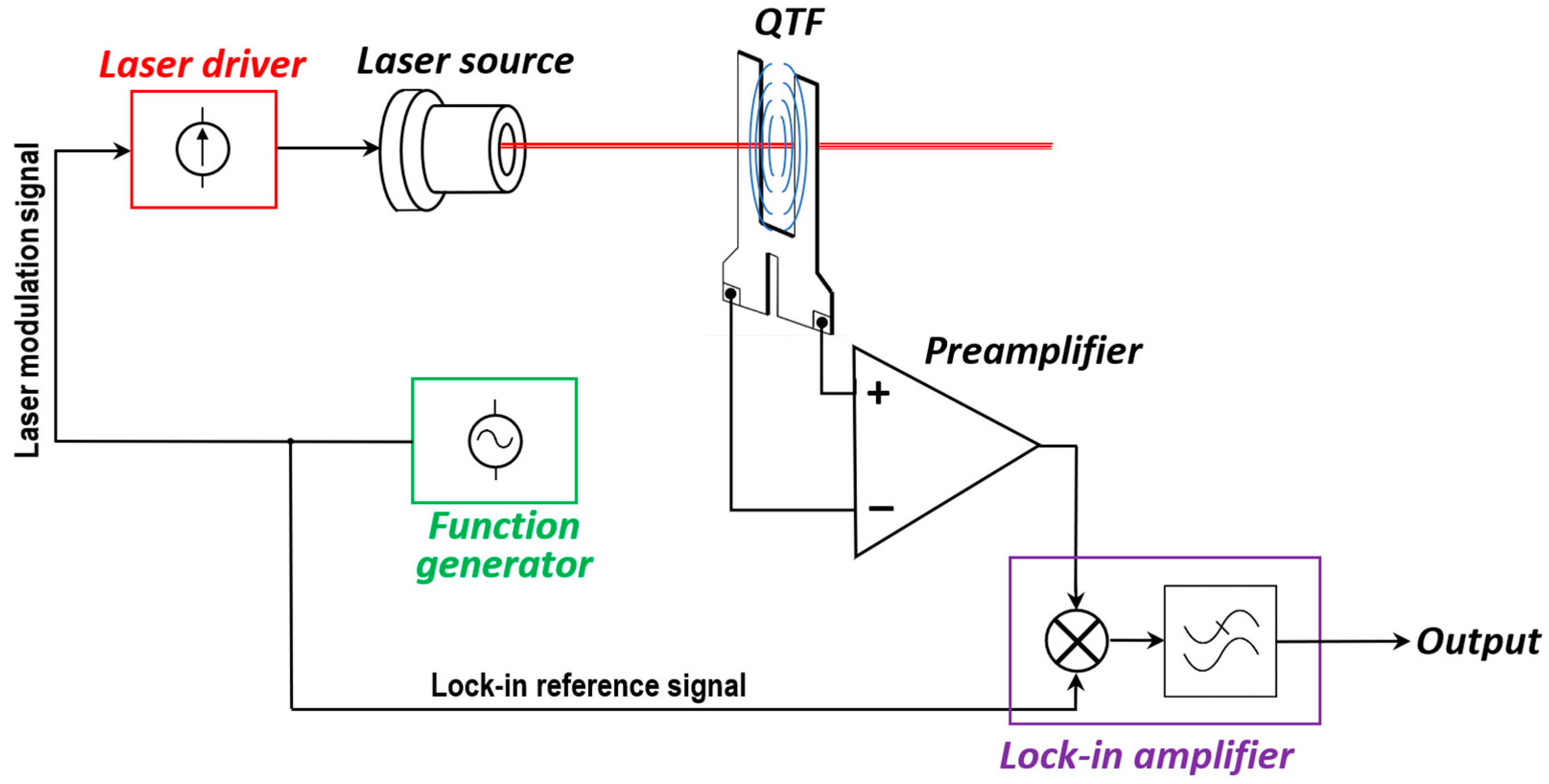
4]. As shown in the schematic diagram of
Figure 1, the intensity of a laser source of suitable wavelength, chosen accordingly to the absorption line of the molecules to be detected, is modulated at a given frequency f
0. Non-radiative, periodic relaxation processes of the gas molecules, excited by the modulated laser light, generate sound waves that are efficiently transformed into electric signals by means of the QTF, if the laser modulation frequency is tuned to the resonant frequency f
s of the crystal or one its sub-harmonics. A lock-in amplifier (LIA) is used to demodulate the signal generated by the QTF and produces a DC output voltage proportional to its amplitude, which, in turns, is proportional to the concentration of the target gas. The QEPAS technique has been proven to be very sensitive and reliable, enabling sub-ppm and even sub-ppb minimum detection limits [
5,
6,
7].
Since the Q factor of typical QTFs used in QEPAS sensors is very high, with an order of magnitude of several thousands [
8], the frequency of the laser modulation signal and the lock-in reference frequency must be carefully selected, to fully exploit the resonance properties of the QTF and maximize the signal-to-noise ratio (SNR) of the sensor.
Although voltage-mode front-end preamplifiers for the QTF have been proposed in the literature [
9,
10,
11,
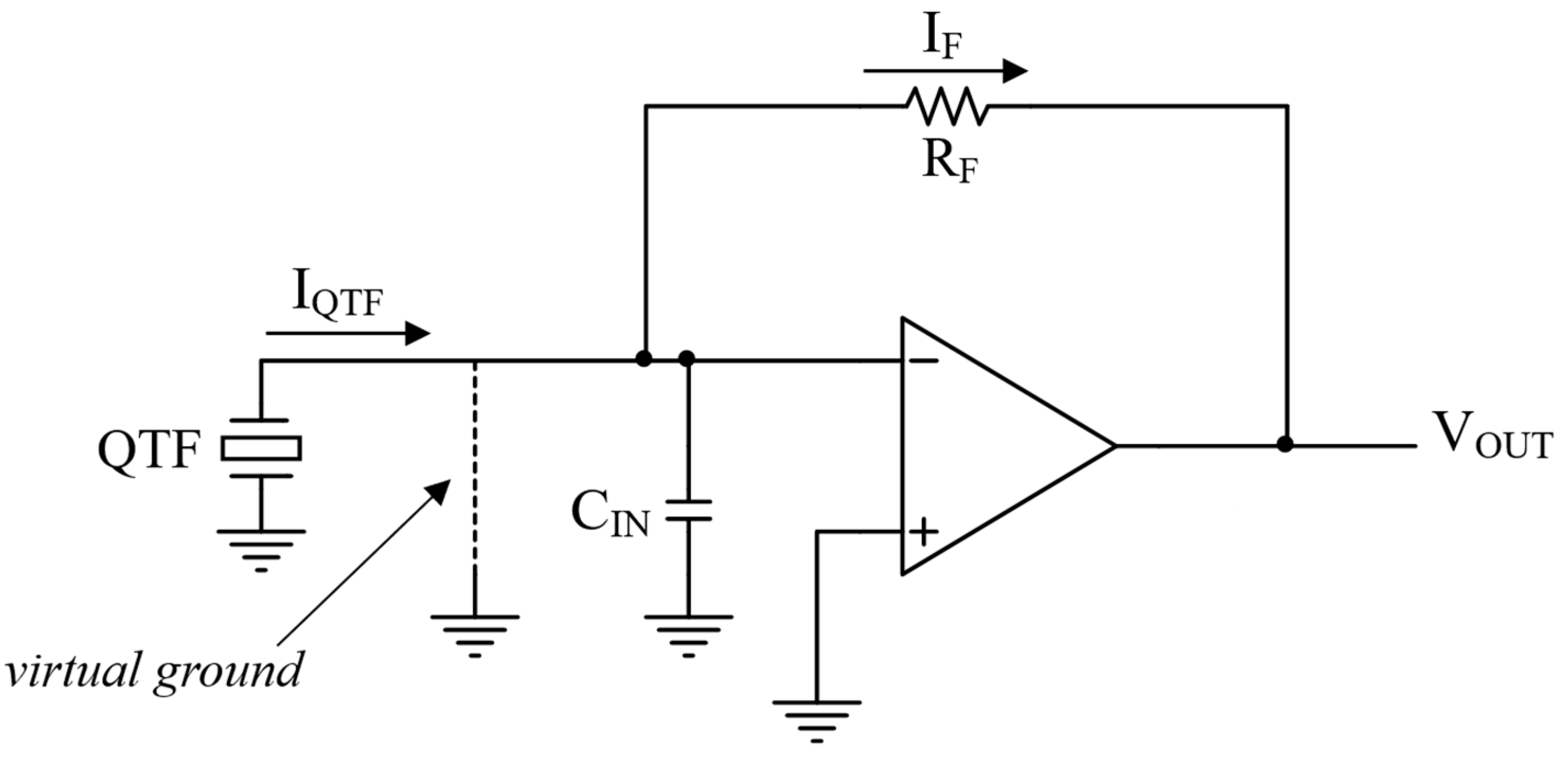
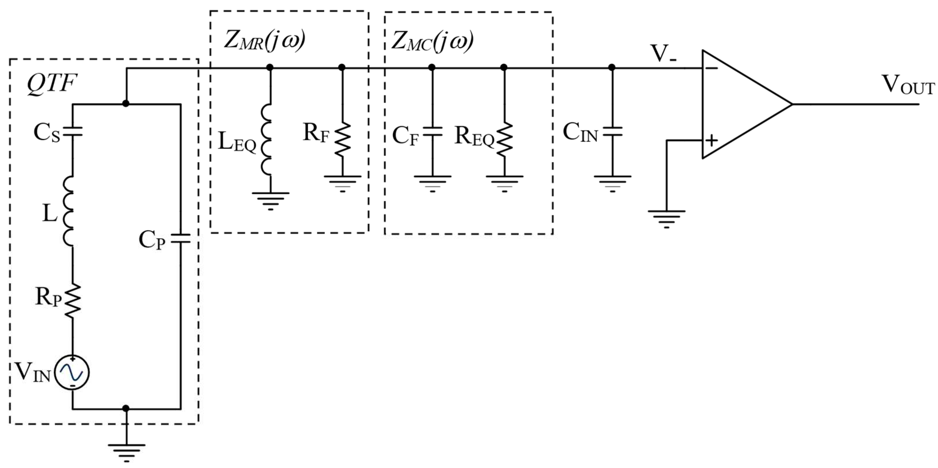
12], the most common circuit configuration for interfacing the QTF is still the classic transimpedance preamplifier (TIA), schematically represented in
Figure 2 [
13,
14,
15,
16].
If the loop gain of the circuit in
Figure 2 is large enough, the inverting input terminal of the operational amplifier (OPAMP) can be considered a virtual ground. This makes the current signal I
QTF generated by the QTF independent of parasitic components, such as the input capacitance of the OPAMP C
IN. Furthermore, the current I
F which flows in the feedback resistor R
F is equal to I
QTF, thus the output signal V
OUT depends only on the characteristics of the piezoelectric sensor and on the value of R
F:
The response of the TIA exhibits a sharp peak at the series resonant frequency f
S of the QTF, which as a consequence, is the most suitable operating frequency for the QEPAS sensor. The value of this frequency is usually identified using the same TIA, by disconnecting from ground the QTF terminal, applying a sinusoidal voltage signal to this terminal and scanning the frequency around the expected value of f
S , until the peak amplitude of V
OUT is reached [
17].
As already pointed out, the ideal behavior of the circuit described above is strictly related to the presence of the virtual ground at the inverting input of the OPAMP, which, in turns, is effective only if the loop gain of the feedback loop is much larger than unity. Usually, in order to guarantee that this condition is fulfilled, it is deemed sufficient to use an OPAMP with a gain-bandwidth product (GBW) much higher than the operating frequency. For instance, in case of a classic QTF with f
S=32.768 kHz, often low-noise OPAMPs with GBW of a few MHz have been used [
9,
10,
12]. In this work, we demonstrate that, due to the behavior of the QTF around its resonant frequency, much larger values of the GBW are needed to guarantee a good virtual ground for the TIA at these frequencies. In case an amplifier with an insufficient bandwidth is used, some undesirable phenomena occur. First, the peak frequency of the circuit response f
peak is no more located at the intrinsic f
S of the QTF, but is shifted to lower frequencies, thus the characterization procedure described above is no more able to provide the intrinsic resonance frequency of the piezoelectric sensor. Moreover, some contributions to the total output noise are strongly affected by the missing virtual ground and, as a consequence, the operating frequency where the maximum SNR is obtained can be different from the frequency f
peak. Thus, in this case, the characterization procedure is no more able to provide the optimal value for the operating frequency of the QEPAS sensor. In any case, it will be shown that the SNR performance obtained are sub-optimal, if compared to the ones that it is possible to achieve if an OPAMP with the same noise characteristics but a much larger GBW is used.
2. TIA Loop Gain as a Function of the OPAMP Gain-Bandwidth Product
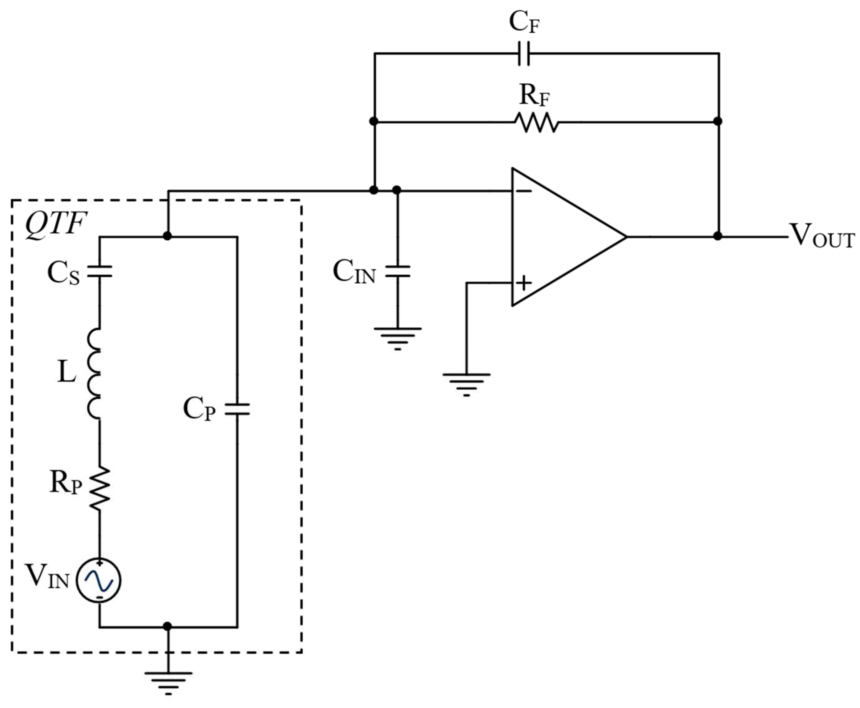
To study the frequency response of the TIA shown in
Figure 2, the QTF can be the described by means of the classic Butterworth-Van Dyke model, with a sinusoidal voltage source V
in inserted in series with the motional arm, composed by R
P, C
S and L, as represented in
Figure 3. Here, V
in represents the electric signal generated by the QTF when the sensor is excited by an acoustic stimulus, due to the piezoelectric effect. In
Figure 3 the QTF model is coupled to the TIA, where the resistor R
F sets the closed loop gain of the circuit, C
F accounts for the parasitic capacitance in parallel to the feedback resistor and C
IN is the input capacitance of the OPAMP.
A typical set of values for the passive components of the circuit in
Figure 3 is reported in
Table 1. With these parameters, the series resonant frequency of the QTF
is 32.768 kHz and its Q factor
is about 10
4. A conservative value of 50fF has been assumed for the parasitic capacitance C
F associated to a surface mount resistor [
18]. A large value of R
F has been considered, to reduce the contribution of the feedback resistor to the total equivalent input noise of the circuit [
19]. In the following, these parameter values will be used for all the simulations, except the input capacitance of the OPAMP, which depends on the specific considered device.
If the loop gain of the circuit in
Figure 3 is very large, so that the inverting terminal of the OPAMP can be considered a good virtual ground, the total capacitance C
P+C
IN=C
PTOT is short circuited and does not give any contribution to the transfer function H(jω)=V
OUT/V
IN of the circuit. The modulus squared of this transfer function is expressed as follows [
19]:
where
. Since at this frequency the reactances of L and C
S are equal and opposite, they cancel each other and the function |H(jω)|
2 exhibits a peak:
Note that C
F has been neglected in equations (2) and (3), since ω
Z=1/(R
FC
F) is much higher than
. We conclude that the most suitable operation frequency for the QEPAS system is the series resonant frequency of the QTF, where the response of the circuit to an acoustic excitation is maximized.
As already pointed out, equations (2) and (3) hold true only if the loop gain T of the circuit is much greater than unity. Thus, it is important to evaluate this parameter around the series resonant frequency of the QTF, in order to understand the conditions which must be fulfilled to validate the above analysis. The transfer function T(s), can be obtained by multiplying the differential gain of the OPAMP A
DM(s) by the voltage divider formed by the impedance of the QTF, Z
QTF, and the feedback impedance R
F//(1/sC
F):
The following expression is obtained, neglecting C
S and C
F with respect to C
PTOT:
Typically, A
DM(s) is a single-pole transfer function with a very low cut-off frequency f
0, due to OPAMP internal compensation. For frequencies higher than the cut-off, the differential gain of the OPAMP can be expressed as a function of the frequency as follows:
where A
0 is the DC gain of the amplifier and GWB=A
0⋅ω
0 is its gain-bandwidth product. The transfer function of equation (5) contains a zero at ω
Z, due to the presence of the small capacitance C
F, which makes acceptable the phase margin of the circuit.
If, for instance we use the OP27 [
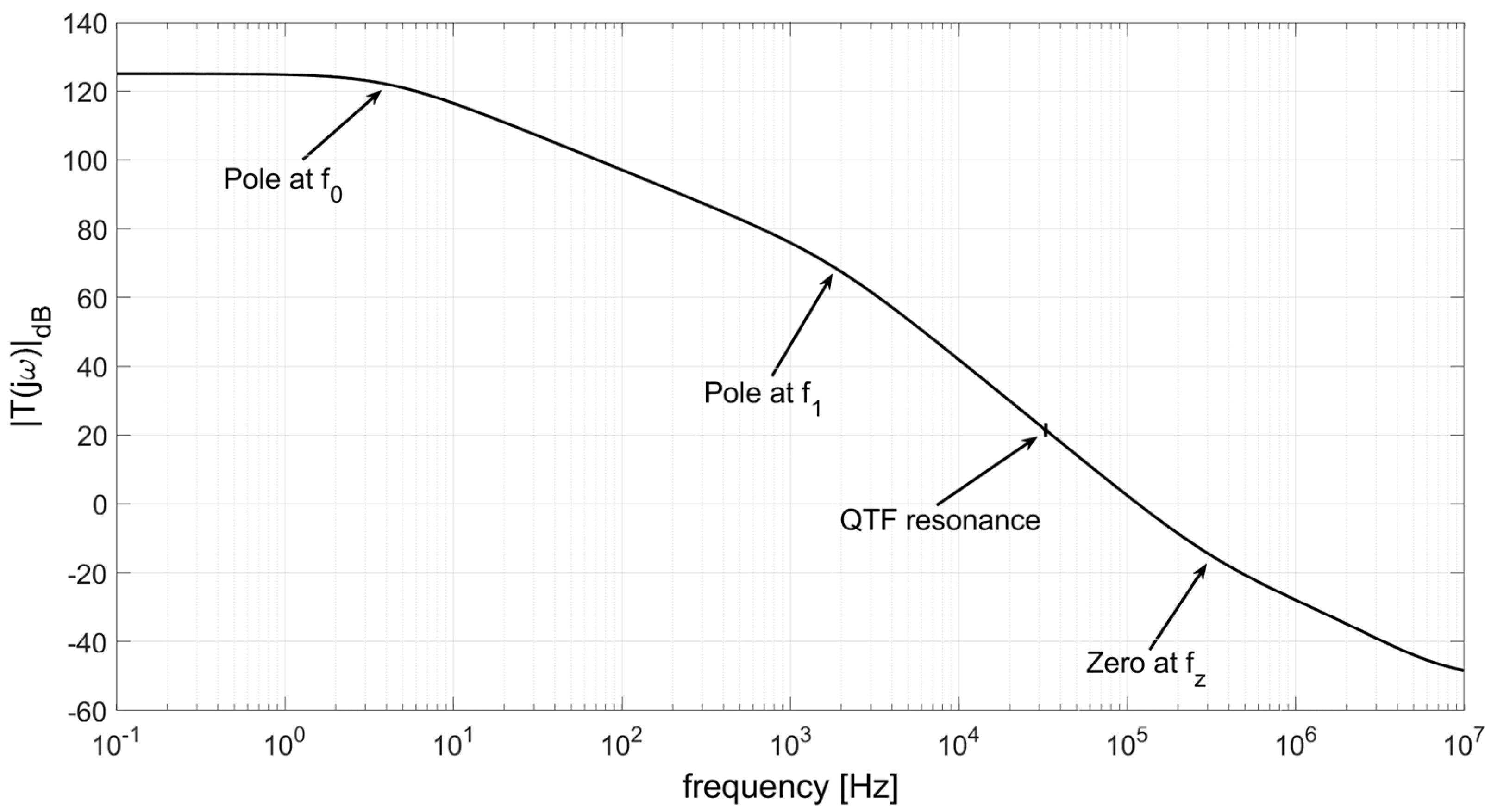
10], an OPAMP with a gain-bandwidth product of about 8 MHz, the result of a broadband SPICE simulation of the magnitude of the loop gain |T(jω)| as a function of the frequency is shown in
Figure 4.
Figure 4 has been generated by simulating 1000 point per decade and, as a consequence, the effects of the QTF resonance, confined in a very narrow band around 32.768 kHz, are barely visible. Instead, the main singularities of T(s), i.e., the dominant pole of the OPAMP at f
0≅4 Hz, a low frequency pole at f
1≅1/(2πR
FC
PTOT)≅1.8 kHz and the zero at f
Z=1/(2πR
FC
F)≅318 kHz are clearly visible. We can conclude that, due to the presence of the low frequency poles located at f
0 and f
1, the magnitude of the loop gain around f
S is slightly more than 20 dB, despite the GBW of the OPAMP is about two orders of magnitude larger than the QTF resonant frequency.
Let us consider now what happens in correspondence of the frequency f
S, which should be the optimal operating frequency for the QEPAS sensor. Here, the motional branch of the QTF reaches its minimum impedance and can be replaced by the only resistor R
P. With the typical values of the parameters we are considering, the frequency 1/(2πR
PC
PTOT)≅180 kHz is quite large as compared to f
S, so we can neglect the capacitance C
PTOT in parallel with R
P. Thus, the loop gain at f
S is simply evaluated as:
Equation (6) states that the value of |T(jω
S)| is obtained by multiplying the gain of the OPAMP at the resonant frequency of the QTF by the ratio R
P/R
F, which is very small in typical cases, as our one. For instance, if we use the OP27, |T(jω
S)| results to be around 2.3 and the inverting input terminal of the OPAMP cannot be considered a good virtual ground at all. This invalidates equations (2) and (3). An OPAMP with a GBW at least an order of magnitude higher would be needed to have a TIA with a behavior closer to the ideal one.
SPICE simulations of the TIA confirm this result.
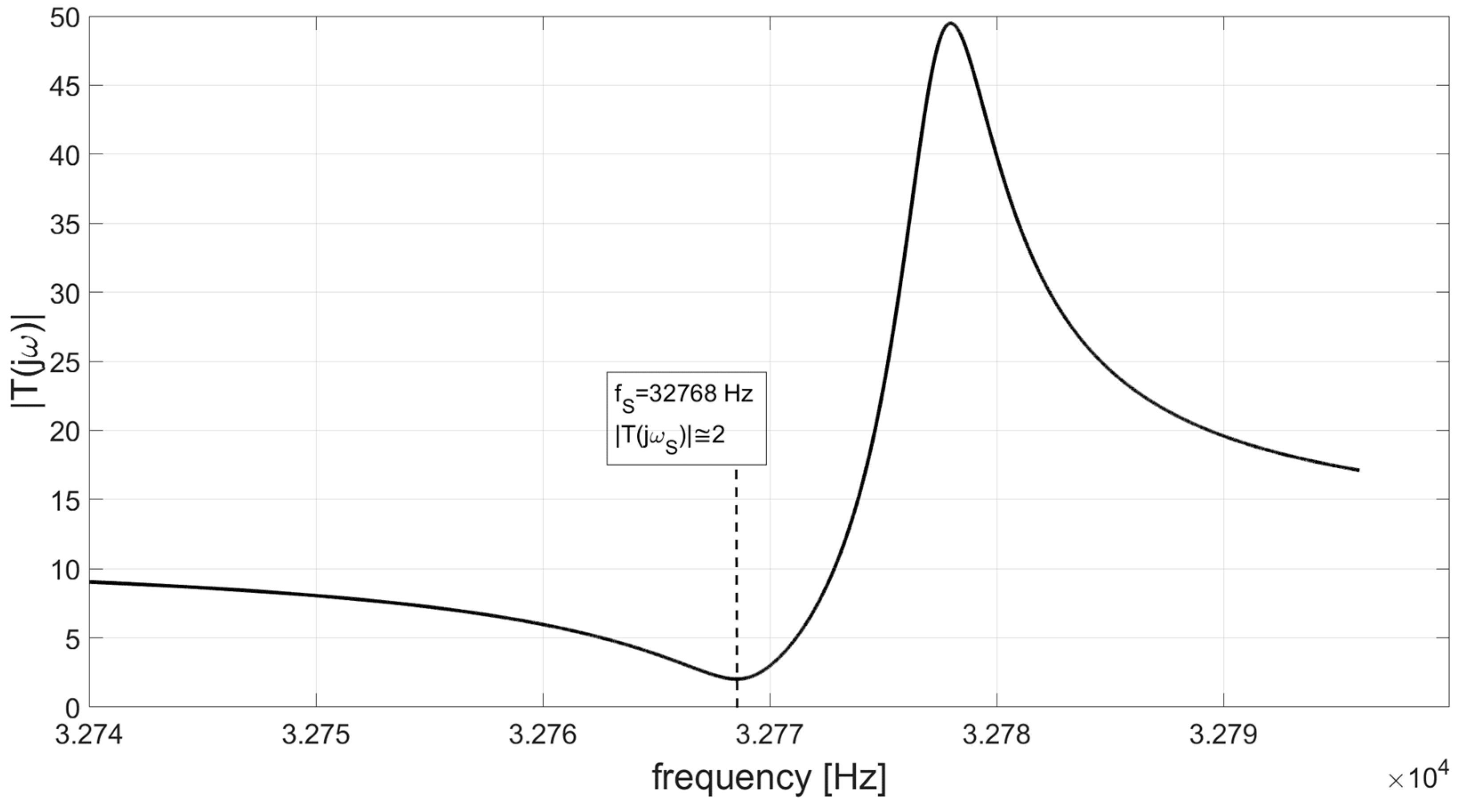
Figure 5 shows the amplitude of the loop gain of the circuit as a function of the frequency in a narrow band around the resonant frequency of the QTF. The value of |T(jω
S)| results to be around 2, very close to the above estimation.
The low value of the loop gain will cause deviations of the TIA response with respect to the ideal one. In turn, this modified behavior affects the choice of the optimal operating frequency for the application of the QEPAS technique, as will be discussed in the next section.
3. Closed-Loop Response of the TIA coupled to the QTF
With a very low value of the loop gain |T(jω
S)|, the analysis of the closed-loop behavior of the circuit in
Figure 3 cannot be carried out considering the presence of the virtual ground. The finite value of the OPAMP gain around the resonant frequency of the QTF must be necessarily taken into account. To study the circuit, we can apply Miller’s theorem [
20] to the feedback impedance Z
F, composed by the parallel of the resistor R
F and the parasitic capacitor C
F. According to this theorem, an equivalent circuit of the TIA is created by replacing Z
F with an impedance Z
M1, placed between the inverting input of the OPAMP and ground, and an impedance Z
M2, connected between the OPAMP output node and ground:
Due to the very low output impedance of the OPAMP, Z
M2 cannot affect the behavior of the circuit and can be omitted. Instead, for what concerns Z
M1, there are two contributions Z
MR and Z
MC in parallel, coming from R
F and C
F, respectively. According to equation (6), Z
MR(jω) is expressed as follows:
and can be considered as the parallel of the resistor R
F with an inductor L
EQ= R
F/GBW.
The contribution of the parasitic capacitance to the input Miller’s impedance is the following:
Z
MC can be considered the parallel of the capacitance C
F with a resistor R
EQ=1/C
FGBW. With the typical values of the parameters shown in
Table 1, using the OP27 (GBW≅2π⋅8x10
6), we obtain L
EQ≅0.2 H and R
EQ≅400 kΩ.
Figure 6 shows the equivalent circuit of the TIA after the application of Miller’s theorem.
Note that C
F << C
PTOT and R
F>>R
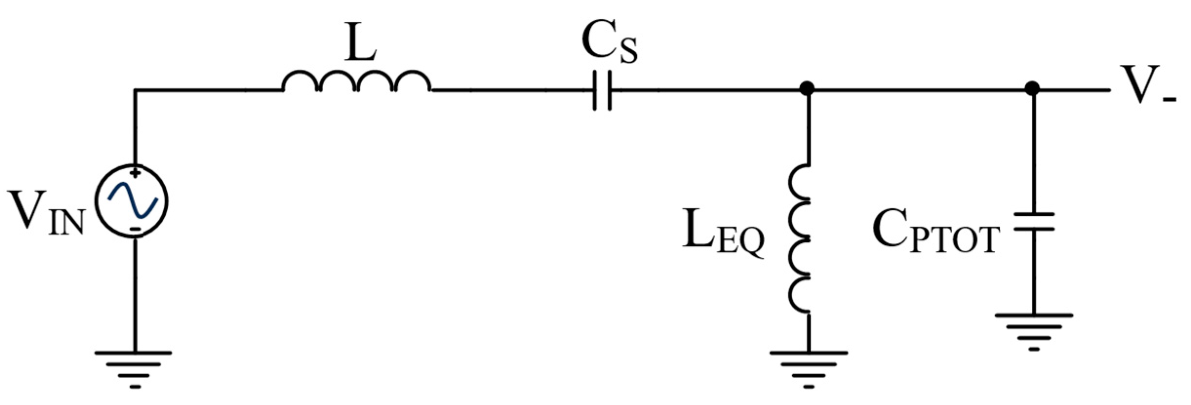
EQ can be neglected. Moreover, the resonant frequencies of the circuit in
Figure 6 are poorly affected by the resistors R
P and R
EQ, thus, in order to find their location, it is sufficient to consider the simplified circuit shown in
Figure 7.
The resonant frequency of the parallel L
EQ-C
PTOT is placed at:
quite higher than f
S. As a consequence, around f
S, this network exhibits an inductive behavior, which slightly shifts the peak of the transfer function |H(jω)| with respect to the expected value f
S. In fact, since around f
S the parallel L
EQ-C
PTOT is equivalent to a frequency-dependent inductor L
X(ω), the transfer function of the circuit in
Figure 7 is the following:
and its peak is located at the frequency f
peak, lower than the series resonant frequency of the QTF:
Of course, the complete transfer function H(jω)=V
OUT/V
IN of the circuit in
Figure 7 is obtained by multiplying V
-/V
IN by the open loop gain of the OPAMP A
DM(jω).
The shift of the peak frequency towards lower values, expressed by equation (11), is confirmed by SPICE simulations of the TIA.
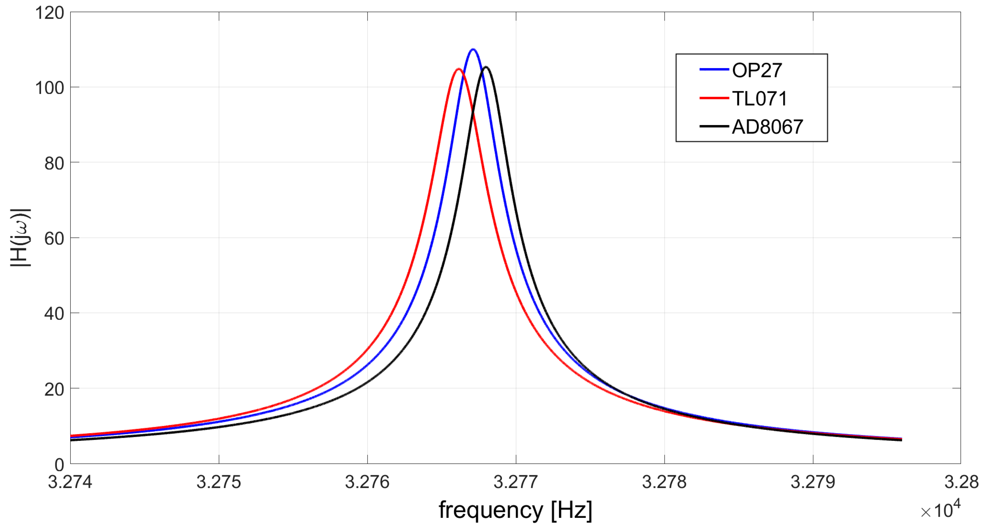
Figure 8 shows the behavior of the modulus of the transfer function H(jω) for three different OPAMPs, listed in
Table 2 together with their gain-bandwidth products and the peak frequency f
peak obtained in simulation.
Table 2 shows that, in case the large bandwidth OPAMP AD8067 is used, the peak frequency of the TIA response coincides with the resonant frequency of the QTF as expected. Instead, with the other two OPAMP models, the shift of f
peak with respect to f
S is apparent and is more pronounced for the slowest OPAMP, the TL071. This shift, of about 0.9 Hz and 1.8 Hz for the OP27 and the TL071 respectively, can be significant in terms of performance of the QEPAS sensor. Note that, if an external sine wave is applied to the QTF coupled to the TIA for the identification of the optimal operating frequency of the QEPAS sensor, as described in the Introduction, the result of the procedure will be always f
peak, different from f
S, in case a too slow OPAMP is used, such as the OP27 or the TL071.
4. Effects of the Limited GBW on the TIA Output Noise
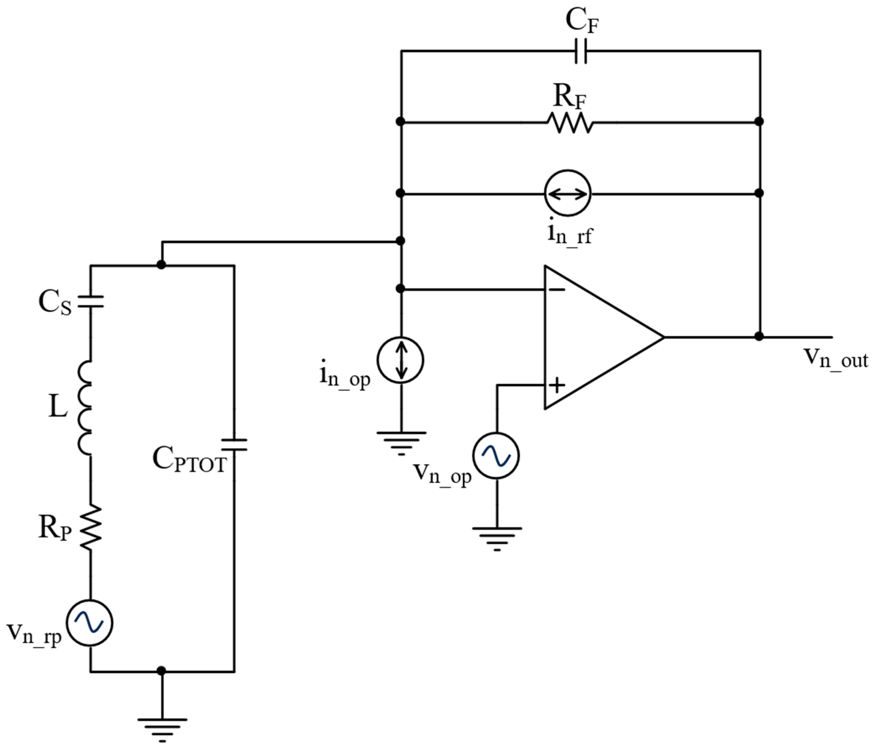
To assess the performance of the TIA used as a front-end for the QTF in a QEPAS sensor, it is mandatory to study the signal-to-noise ratio (SNR) obtained at its output. The main noise sources in the circuit of
Figure 6 are the thermal noise of the resistors R
P and R
F, v
n_rp and i
n_rf respectively, and the equivalent input noise sources of the OPAMP, v
n_op and i
n_op, as represented in
Figure 9.
The total power spectral density of the output noise S
n_out is obtained by summing the contributions given by the power spectral densities of the noise sources in
Figure 9, weighted by the corresponding transfer functions:
where
and k is the Boltzmann constant and T the absolute temperature.
If the gain-bandwidth product of the OPAMP is large enough and its inverting input terminal can be considered a good virtual ground, |H(jω)|
2 is given by equation (2), |H
f(jω)|
2≅R
F2, and
where
and
[
19].
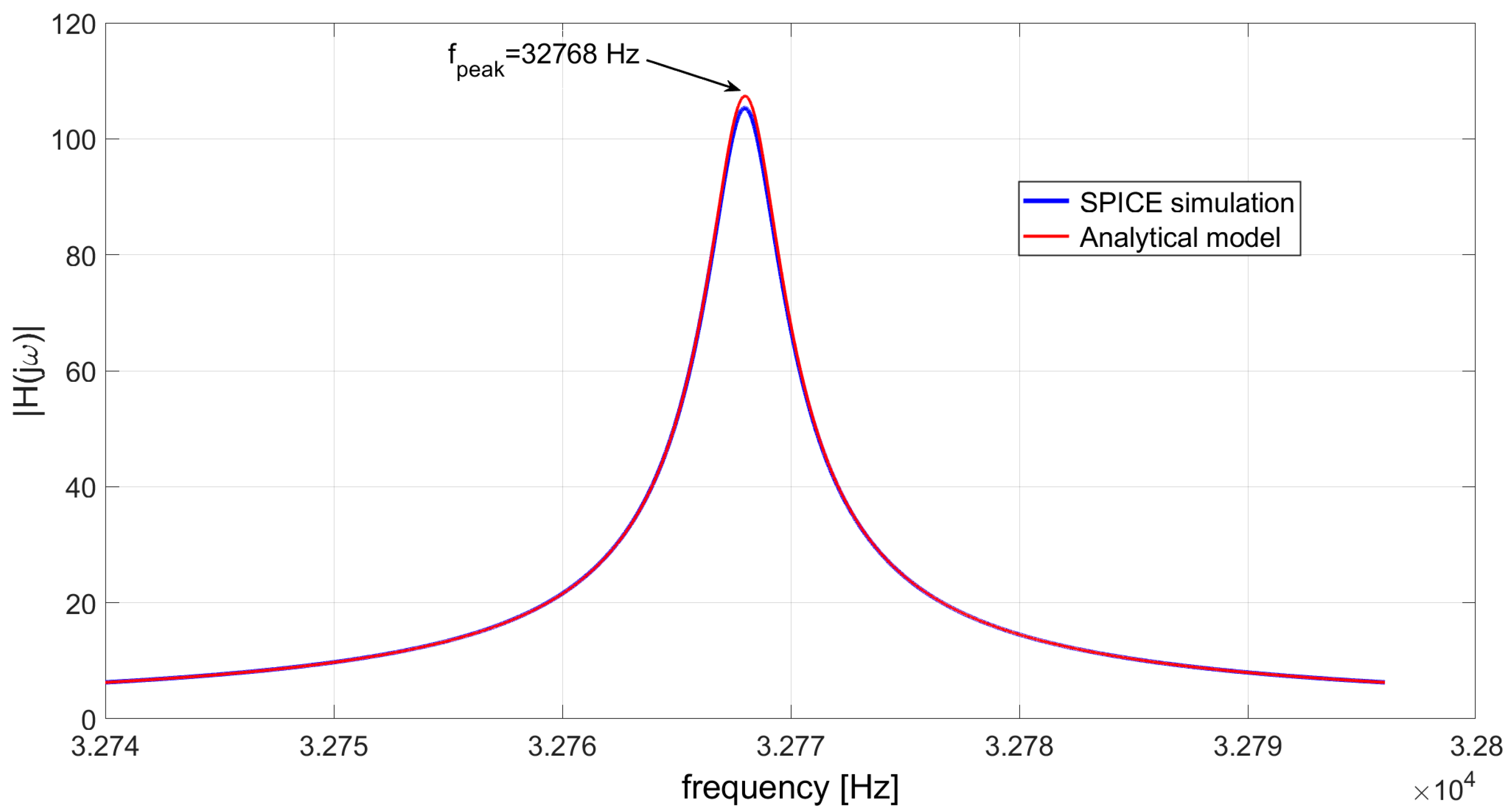
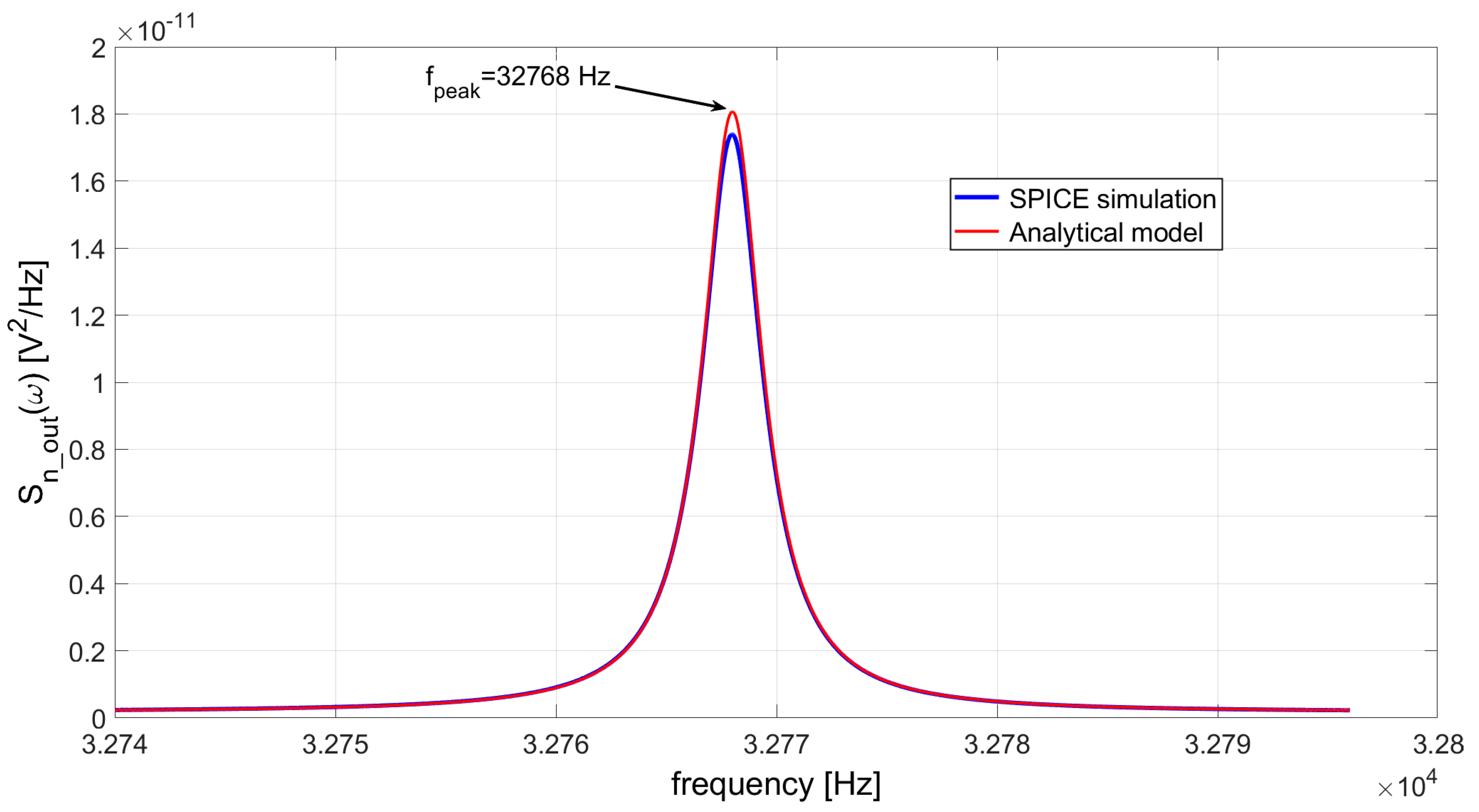
A comparison between the results obtained with SPICE simulations and the analytical model confirms the validity of equations (2) and (12).
Figure 10 shows the modulus of the TIA transfer function |H(jω)|, whereas
Figure 11 displays the total output noise power spectral density of the circuit S
n_out(ω), when the AD8067 is used, in which case the OPAMP inverting input can be considered a good virtual ground. In the analytical model, the values of the equivalent input noise sources of the OPAMP, i
n_op = 0.6 fA/√Hz and v
n_op = 6.6 nV/√Hz, have been derived from its data-sheet. The parameters of the QTF model are the same reported in
Table 1. The analytical model just slightly overestimates the results provided by SPICE simulations, but the frequency f
peak coincides exactly with the series resonant frequency of the QTF f
S=32768 Hz, as expected.
If an OPAMP with a low GBW is used in the TIA, the noise transfer functions which appear in equation (12) are affected by the missing virtual ground at the inverting input of the OPAMP, exactly as happens to |H(jω)|. If, for instance we consider the OP27 and an OPAMP with the same input equivalent noise sources and the same input capacitance C
IN, but much larger GBW, we will observe a different frequency behavior of all the noise contributions in equation (12).
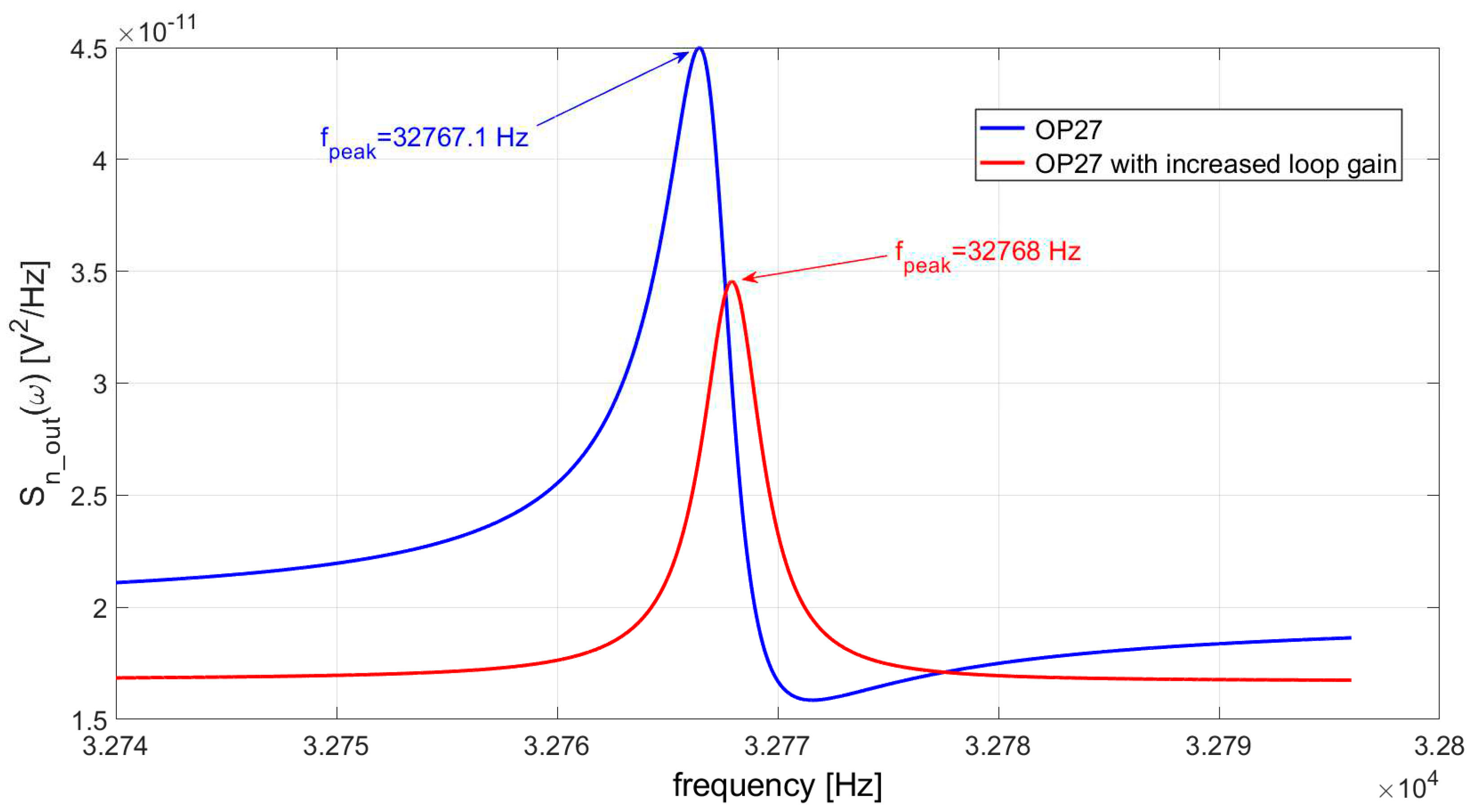
Figure 12 shows a comparison between the total output noise power spectral density S
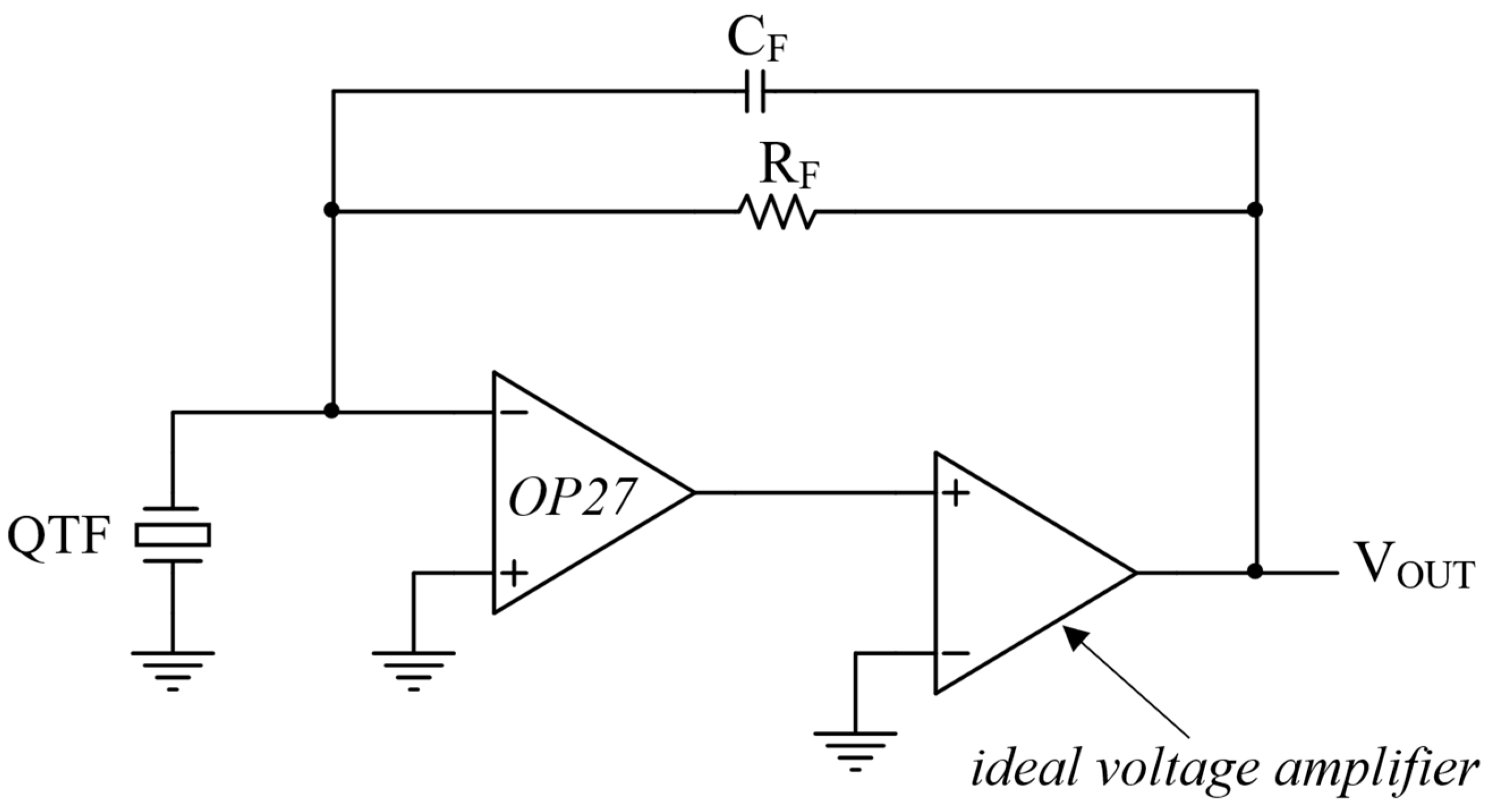
n_out of the TIA realized using the OP27 and the same OPAMP, but with an increased GBW, obtained by inserting an ideal voltage amplifier with gain equal to 20 into the feedback loop of the TIA, at the output of the OPAMP (see
Figure 13).
It is apparent from
Figure 12 that the behavior of S
n_out as a function of frequency is completely different in the two cases, which differ only in the GBW of the OPAMP. In particular, as illustrated by
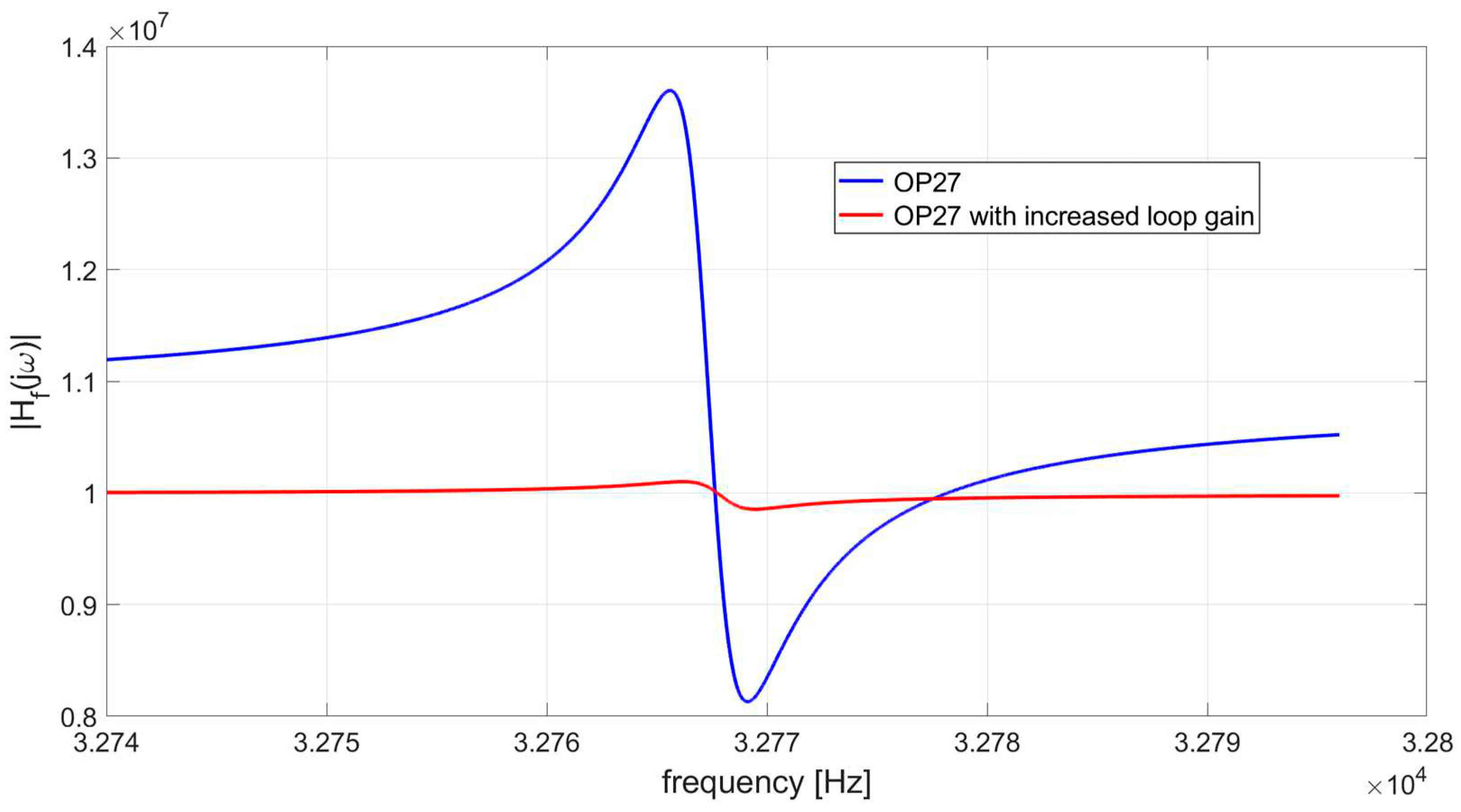
Figure 14, the transfer function H
f(jω) is strongly affected by the absence of a good virtual ground, as well as the contributions to the total output noise due to the equivalent input current noise of the OPAMP and the feedback resistor.
As a consequence, also the behavior of the SNR at the output of the QEPAS sensor will be dependent on the GBW of the OPAMP used in the LIA, other than by its noise performance.
5. Evaluation of the SNR and Effects of the Limited GBW
For the evaluation of the SNR at the output of the QEPAS sensor, the function of the LIA can be considered equivalent to a band-pass filter with narrow bandwidth BW, centered at its reference frequency f
REF [
19,
21]. Thus, assuming a unity amplitude for the input signal V
IN, the SNR at the output of the LIA can be defined as follows:
where V
n_out is the rms value of the output noise, ω
REF=2πf
REF and
is the response of a biquadratic band-pass filter with center frequency f
REF and bandwidth BW=ω
REF/Q
filt, used to simulate the LIA function.
If we want to enhance noise rejection, the bandwidth of the LIA filter must be extremely narrow, i.e. the LIA integration time must be very large. As a consequence, in practice, the squared rms output noise V
n_out(ω
REF)
2 is proportional to the noise power spectral density S
n_out(ω
REF) [
10], and the SNR can be expressed as:
Notice that, in equation (14), the ratios |H
f(jω
REF)|
2/|H(jω
REF)|
2 and |H
vn_op(jω
REF)|
2/|H(jω
REF)|
2 are independent on the GBW of the OPAMP used in the TIA. In other words, if the loop gain of the circuit is increased by adding a gain stage in the feedback loop, as done to obtain
Figure 12 and
Figure 14, these ratios are unaffected, due to the linearity of the system. Thus, equation (14) states that the dependence of the SNR on the LIA reference frequency f
REF is not affected by the GBW of the OPAMP.
Extensive SPICE simulations have been carried out to support this conclusion. A band-pass filter with BW=0.1 Hz has been cascaded to the same TIAs, based on the OPAMP OP27, used to reproduce
Figure 12 and
Figure 13. The SNR at the filter output, expressed by equation (13), has been simulated, by varying the center frequency of the filter by steps of 0.1 Hz around the resonance of the QTF, in the interval from 32758 Hz to 32776 Hz.
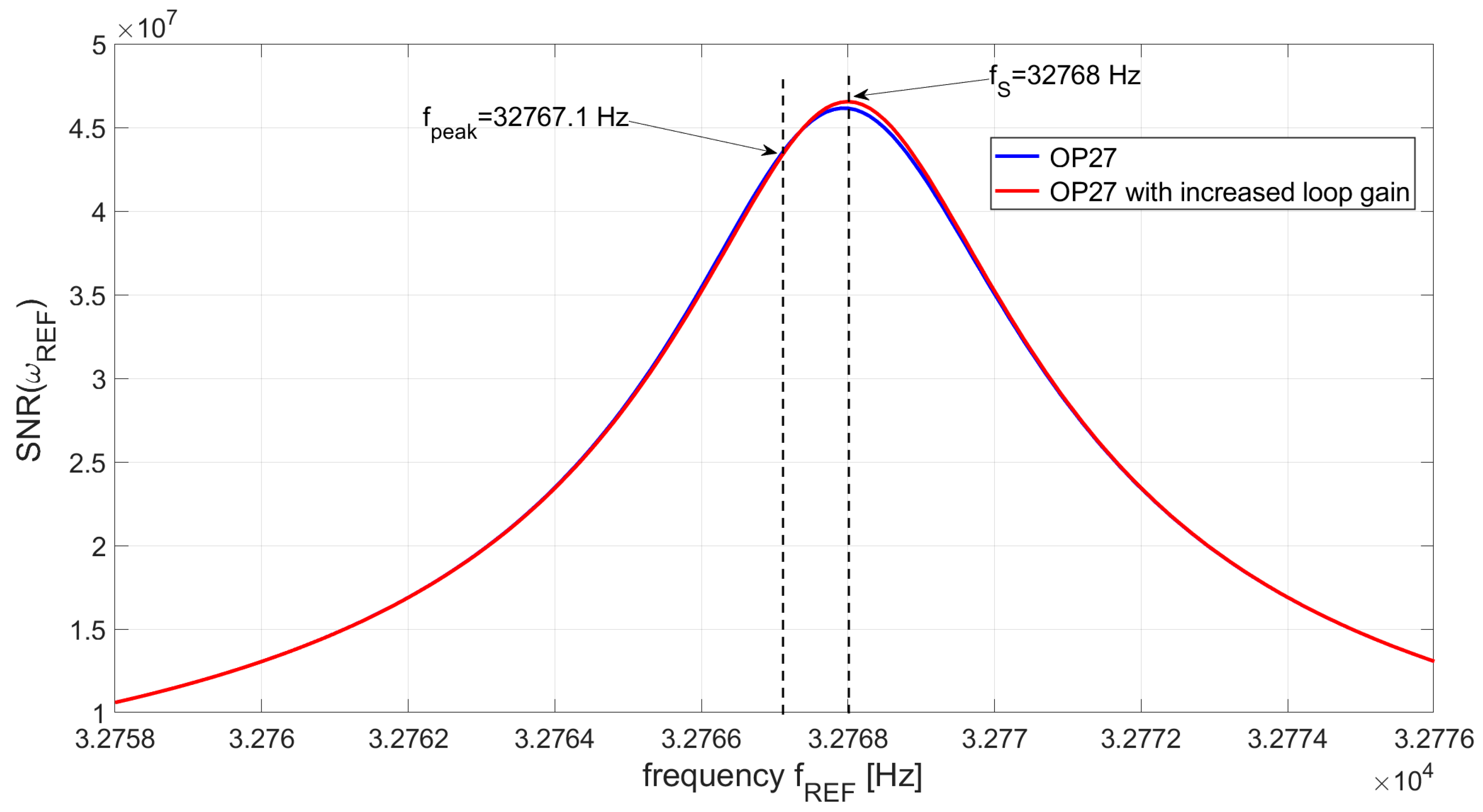
Figure 15 shows the behavior of the SNR, obtained with and without boosting the GBW of the OPAMP by means of an ideal voltage amplifier with gain 20. As expected, the increase of the loop gain of the TIA does not affect too much the behavior of the SNR and, in particular, does not modifies the value of the reference frequency corresponding to the peak of the SNR, which remains almost coincident with the series resonant frequency of the QTF, f
S. This means that the optimal operating frequency for the QEPAS sensor is f
S, which is different from f
peak, i.e. the frequency where the peak of the signal is obtained, in case the OP27 is used for the TIA. As a consequence, if the QEPAS sensor is operated at the frequency f
peak, an appreciable penalty in terms of SNR results, as highlighted in
Figure 15. Thus, we can conclude that, for very long integration time of the LIA, the use of a TIA realized with an OPAMP with limited GBW, like the OP27 or the TL071, leads to a nonoptimal choice of the operating frequency of the QEPAS sensor.
Since the shift of fpeak with respect to fS increases for decreasing values of GBW, using an OPAMP such as the TL071 (GBW=3 MHz) would result in larger penalties in terms of SNR, if the chosen operating frequency of the QEPAS sensor is fpeak instead of fS.
When we need to increase the rate of the measurements, the bandwidth of the LIA filter must be increased as well. The noise power spectral density is integrated in a larger bandwidth around the LIA reference frequency and the peak of the SNR at the LIA output tends to move close to the peak frequency of the signal f
peak, thus the choice of the operating frequency of the QEPAS sensor is near to the optimal one. Nevertheless, the maximum SNR achievable is well below the one that can be obtained keeping the same noise performance of the OPAMP but increasing its GBW, so that the optimal operating frequency and the signal peak frequency f
peak both coincide with f
S. This is illustrated in
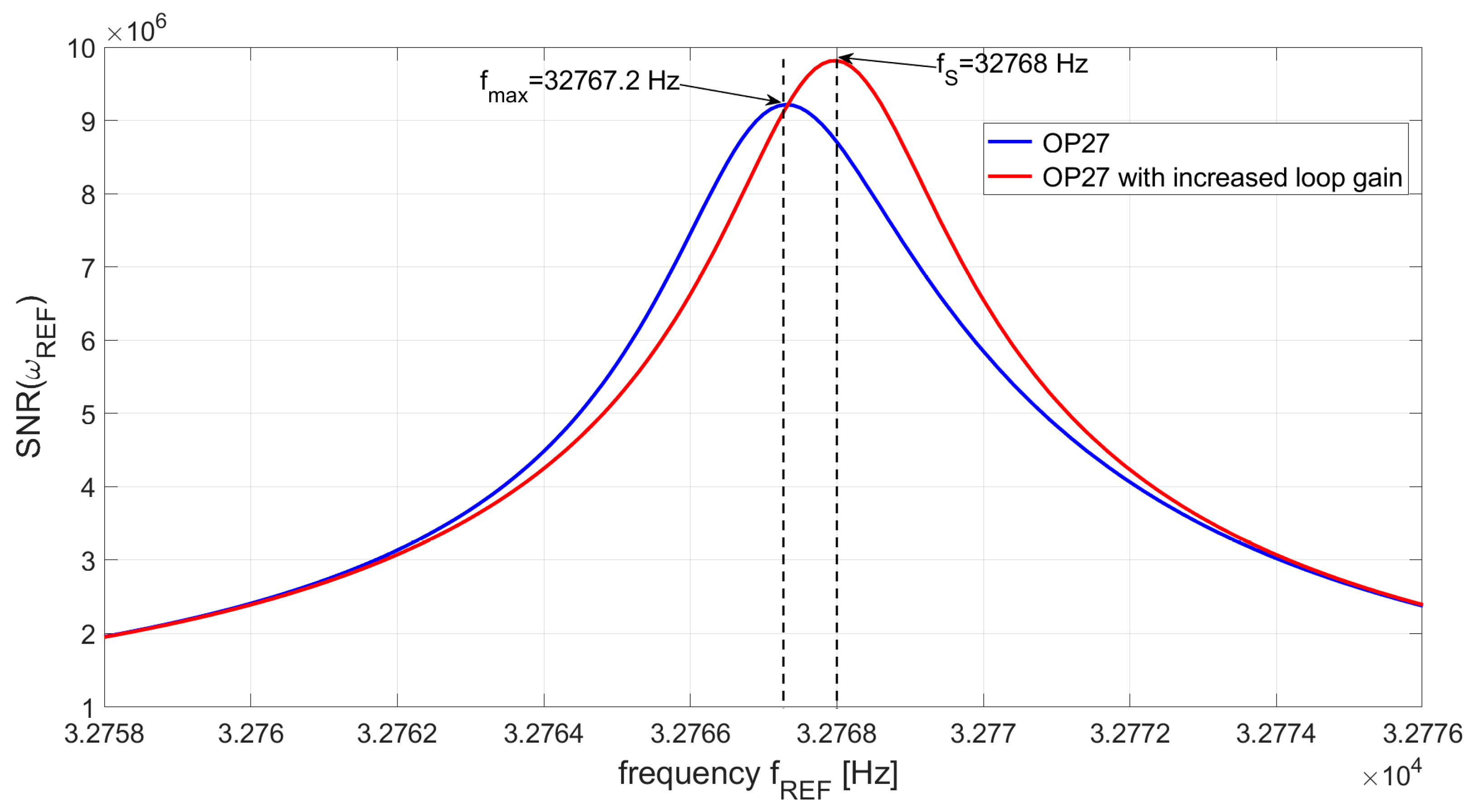
Figure 16, where the simulated behavior of the SNR as a function of the LIA reference frequency is shown for a filter bandwidth of 3 Hz and a TIA based on the OPAMP OP27, with and without boosting of the loop gain.
If the sheer OP27 is used, the frequency corresponding to the peak of the SNR is fmax=32768.2 Hz, very close to fpeak=32768.1 Hz, but the maximum value of the SNR is about 9.2e6, which is less than the value that is possible to achieve when the GBW is increased by a factor of 20, equal to about 9.8e6. So, also in this case, the best performance that is possible to achieve with the QEPAS sensor is once again limited by the small GBW of the OPAMP used in the TIA.
6. Conclusions
The analog front-end of the QTF, in a typical QEPAS sensor, is a transimpedance amplifier realized with a low-noise OPAMP. We have shown that, even though the gain-bandwidth of the OPAMP is two order of magnitude larger than the series resonant frequency of the QTF, this can be insufficient to guarantee that the preamplifier works as expected in terms of closed loop behavior, due to the remarkable attenuation introduced in the loop gain of the circuit by the QTF around its series resonant frequency fS. The effect of the low value of the loop gain around fS is a shift of the frequency fpeak corresponding to the peak of the TIA output signal with respect to the expected value fS. As a consequence, in this case fpeak ≠ fS is chosen as reference frequency for the LIA. When the LIA filter is very selective, in order to reject the noise as much as possible and increase the sensitivity of the QEPAS sensor, this turns out to be a wrong choice, since the operating frequency corresponding to the maximum value of the SNR at the LIA output is fS, not fpeak. On the other hand, when the integration time of the LIA is decreased, to increase the measurement rate, the choice of fpeak as QEPAS operating frequency is correct, but the maximum achievable value of the SNR is lower than the one which can be obtained using in the TIA an OPAMP with the same noise performance, but with much larger GBW. In conclusion, the OPAMP must be selected not only considering its noise characteristics, but also a GBW sufficiently high to guarantee a large value of the TIA loop gain. In this respect, OPAMPs with higher GBW are needed especially in case the quality factor of the QTF is very large, which corresponds to low values of the resistance Rp, and the TIA feedback resistor is increased, to reduce its noise contribution and increase the closed loop gain of the circuit.
Figure 1.
Simplified block diagram of a QEPAS sensor.
Figure 1.
Simplified block diagram of a QEPAS sensor.
Figure 2.
QTF read-out by means of a transimpedance preamplifier.
Figure 2.
QTF read-out by means of a transimpedance preamplifier.
Figure 3.
Butterworth-Van Dyke model of the QTF coupled to the TIA.
Figure 3.
Butterworth-Van Dyke model of the QTF coupled to the TIA.
Figure 4.
SPICE simulation of the loop gain of the TIA in
Figure 2, with the OPAMP OP27.
Figure 4.
SPICE simulation of the loop gain of the TIA in
Figure 2, with the OPAMP OP27.
Figure 5.
Detail of the frequency behavior of |T(jω)| around the resonant frequency of the QTF, for the TIA based on the OP27 OPAMP.
Figure 5.
Detail of the frequency behavior of |T(jω)| around the resonant frequency of the QTF, for the TIA based on the OP27 OPAMP.
Figure 6.
Equivalent circuit of the TIA after the application of Miller’s theorem to the feedback impedance.
Figure 6.
Equivalent circuit of the TIA after the application of Miller’s theorem to the feedback impedance.
Figure 7.
Simplified circuit for the evaluation of the resonant frequencies of the circuit in
Figure 6.
Figure 7.
Simplified circuit for the evaluation of the resonant frequencies of the circuit in
Figure 6.
Figure 8.
Frequency response of the TIA realized with three different OPAMPs.
Figure 8.
Frequency response of the TIA realized with three different OPAMPs.
Figure 9.
Main noise sources in the TIA.
Figure 9.
Main noise sources in the TIA.
Figure 10.
TIA realized with the AD8067: modulus of the transfer function |H(jω)| obtained with SPICE simulations and equation (2).
Figure 10.
TIA realized with the AD8067: modulus of the transfer function |H(jω)| obtained with SPICE simulations and equation (2).
Figure 11.
TIA realized with the AD8067: total output noise power density obtained with SPICE simulations and equation (12).
Figure 11.
TIA realized with the AD8067: total output noise power density obtained with SPICE simulations and equation (12).
Figure 12.
Comparison between the output noise power spectral densities of the TIA realized with the OP27 and with the same OPAMP, but with loop gain increased by a factor of 20, by means of an ideal voltage amplifier inserted in the feedback loop.
Figure 12.
Comparison between the output noise power spectral densities of the TIA realized with the OP27 and with the same OPAMP, but with loop gain increased by a factor of 20, by means of an ideal voltage amplifier inserted in the feedback loop.
Figure 13.
Increasing the loop gain of the TIA based on the OP27, by inserting an ideal voltage amplifier in the feedback loop.
Figure 13.
Increasing the loop gain of the TIA based on the OP27, by inserting an ideal voltage amplifier in the feedback loop.
Figure 14.
Comparison between the modulus of the transfer function Hf(jω) of the TIA realized with the OP27 and with the same OPAMP, but with loop gain increased by a factor of 20.
Figure 14.
Comparison between the modulus of the transfer function Hf(jω) of the TIA realized with the OP27 and with the same OPAMP, but with loop gain increased by a factor of 20.
Figure 15.
SNR at the LIA output as a function of the LIA reference frequency: LIA filter bandwidth BW=0.1 Hz, TIA realized with the OP27 and with the same OPAMP, but with loop gain increased by a factor of 20.
Figure 15.
SNR at the LIA output as a function of the LIA reference frequency: LIA filter bandwidth BW=0.1 Hz, TIA realized with the OP27 and with the same OPAMP, but with loop gain increased by a factor of 20.
Figure 16.
SNR at the LIA output as a function of the LIA reference frequency: LIA filter bandwidth BW=3 Hz, TIA realized with the OP27 and with the same OPAMP, but with loop gain increased by a factor of 20.
Figure 16.
SNR at the LIA output as a function of the LIA reference frequency: LIA filter bandwidth BW=3 Hz, TIA realized with the OP27 and with the same OPAMP, but with loop gain increased by a factor of 20.
Table 1.
Values of the passive components of the circuit in
Figure 2.
Table 1.
Values of the passive components of the circuit in
Figure 2.
| Parameter |
Value |
| Cp
|
5 pF |
| CS
|
5.2424 fF |
| L |
4.50 kH |
| Rp
|
92.65 kΩ |
| Cin
|
4 pF |
| RF
|
10 MΩ |
| CF
|
50 fF |
Table 2.
OPAMP models used for the SPICE simulations.
Table 2.
OPAMP models used for the SPICE simulations.
| OPAMP |
Gain-Bandwidth Product [MHz] |
Peak Frequency fpeak [Hz] |
| OP27 |
8 |
32767.1 |
| TL071 |
3 |
32766.2 |
| AD8067 |
300 |
32768.0 |
