Preprint
Review

Integrated Photonic Sensors with Enhanced Evanescent Field: Unveiling the Dynamic Interaction with the Ambient Medium

Altmetrics

Downloads

204

Views

44

Comments

0

A peer-reviewed article of this preprint also exists.

This version is not peer-reviewed

Submitted:

06 February 2024

Posted:

06 February 2024

You are already at the latest version

Alerts
Abstract
Photonic sensors are innovative devices that leverage the principles of light-matter interaction to enable precise and efficient detection of various physical parameters. These sensors operate by exploiting the interaction between photons, the fundamental particles of light, and matter. The light propagates through an optical waveguide, and a portion of the electromagnetic field extends beyond the waveguide surface, forming the evanescent field. This evanescent field interacts with the surrounding medium, allowing for highly sensitive detection of changes in the refractive index or properties of nearby substances. The underlying concept involves the modulation of light properties, such as intensity, wavelength, or phase, when it interacts with a target substance or undergoes changes in the surrounding environment. The advancements in photonic sensor technology have paved the way for enhanced sensitivity, selectivity, and miniaturization, making them invaluable tools in diverse industries. The ability to harness light-matter interactions for sensing purposes not only facilitates highly sensitive measurements but also allows for non-intrusive and remote monitoring, contributing to the evolution of smart and connected systems. In this overview, the material platforms and waveguide structures are explored that can make highly sensitive photonic devices applied to gas and biosensing applications.
Keywords: 
Subject: Physical Sciences  -   Optics and Photonics

1. Introduction

Photonic sensors based on optical waveguides (WGs) operate at the forefront of cutting-edge technology, leveraging the fundamental principle of guided light propagation to establish a sophisticated mechanism for exceptionally sensitive and specific environmental monitoring [1,2]. Photonic sensors based on evanescent field principles represent a sophisticated and versatile class of optical sensing devices [3]. These sensors exploit the evanescent field, an electromagnetic wave that extends just beyond the surface of a material, to detect changes in the surrounding environment. In these systems, light is typically coupled into a WG or optical fiber, permitting the evanescent field to interact with the adjacent medium. The interaction induces alterations in the transmitted light, such as changes in intensity or wavelength, which are then precisely assessed. This modulation in the optical signal serves as a sensitive indicator for variations in the targeted parameters, such as refractive index, temperature, or the presence of specific biomolecules. Photonic sensors based on evanescent field principles find applications in a myriad of fields, ranging from biochemistry and medical diagnostics to environmental monitoring and industrial sensing [4,5,6]. Their high sensitivity, real-time monitoring capabilities, and non-invasive nature make them vital tools for progressing our capabilities in precision sensing and measurement technologies.
Optical WG biochemical sensing represents a convergence of optical WG technology with biological and chemical methodologies. Within the realm of chemical sensors, biosensors specifically play a pivotal role in this interdisciplinary field. Optical biochemical sensing can be categorized into labelled and unlabelled approaches, with refractive index sensing being an example of the latter. In the context of optical WG biochemical sensors, alterations in the evanescent field induced by changes in parameters like refractive index and absorption coefficient occur. Typically, these changes stem from variations in the phase of transmitted light, leading to a distinct effective refractive index in the optical transmission mode. The mode coupling theory, applicable to sensors like surface plasmon resonance (SPR) and grating sensors, is employed to calculate the resultant change in effective refractive index [7,8,9]. This calculation method extends to devices such as microring resonators (MRRs) [10,11], Mach–Zehnder interferometers (MZIs) [12], multimode interferences (MMIs) [13,14], fiber Bragg gratings [15], photonic crystals [16], and other differential interferometers [17].
Utilizing the refractive index change or absorption spectrum, optical WG refractive index biochemical sensors enable qualitative or quantitative analyses of gases, liquids, and solid substances in testing scenarios. Beyond that, these sensors find application in detecting harmful gas concentrations in the environment, monitoring food and water quality, and identifying bacteria and viruses for public health concerns and chemical threat perception [8]. The label-free detection mechanism employed by biochemical sensors relies on the change in refractive index caused by molecular interactions. This approach is particularly advantageous for measuring chemical substances, viruses, or bacteria, as it is directly correlated with the target sample concentration or surface density. Notably, this method is both cost-effective and straightforward, making it a valuable tool in various analytical applications [18].
Within the literature, numerous photonic sensors have been exemplified, showcasing their reliance on the intricate mechanism of the evanescent field [19,20,21,22]. These sensors leverage the unique properties of the evanescent field to achieve enhanced sensitivity and precision in detecting changes in the surrounding environment. The diverse applications of these sensors encompass fields such as biomedical research, environmental monitoring, and industrial processes. By exploiting the evanescent field, these photonic sensors provide a robust foundation for advancing sensing technologies, offering innovative solutions with broad implications for scientific research and practical applications [23,24,25,26,27]. This review systematically delves into the nuanced concept of the evanescent field ratio in Section 2, elucidating its critical role in the development of highly sensitive photonic devices. Section 3 meticulously explores diverse WG geometries, offering a comprehensive analysis of their potential applications in realizing heightened sensitivity. Moving forward, Section 4 delves into the material platforms, providing a discerning examination of their significance in relation to the evanescent field ratio. Section 5 delves into practical implementations, focusing on two prevalent applications—gas sensing and biosensing—where the evanescent field of the WG mode becomes instrumental. The paper culminates with insightful concluding remarks in Section 6, summarizing key findings and paving the way for future advancements in the realm of evanescent field-based sensing technologies.

2. Concept of evanescent field ratio

The evanescent field of a mode propagating in a WG is a crucial concept in the study of electromagnetic waves and their behavior within confined structures. The evanescent field refers to the portion of the electromagnetic field that extends beyond the core of the WG into the surrounding medium. Unlike the propagating field, which carries energy along the WG axis, the evanescent field decays exponentially as it moves away from the core [28]. This phenomenon arises due to the total internal reflection of the mode within the WG, causing the electromagnetic field to extend into the adjacent medium. The evanescent field plays a crucial role in various applications, including sensing and WG-based devices, where interactions with the surrounding medium or nearby structures are essential for functionality [29,30,31]. The graphical illustration of the evanescent field of the WG mode interacting with the ambient medium is shown in Figure 1. Understanding and manipulating the evanescent field is fundamental for optimizing the performance of such devices [32].
The evanescent field ratio (EFR) is a parameter that characterizes the strength of the evanescent field compared to the total field in a WG. It is particularly significant in the study of guided electromagnetic modes, such as those in optical fibers or other confined structures. The EFR is calculated by determining the proportion of the total field that comprises the evanescent field. Mathematically, it is expressed as the square of the amplitude of the evanescent field divided by the square of the amplitude of the total field. This ratio provides insights into the extent to which the electromagnetic energy associated with a mode is confined within the WG core and the degree to which it penetrates the surrounding medium. A higher EFR indicates a more pronounced influence of the evanescent field, which is crucial in applications such as sensing, where interactions with the external environment play a vital role in device performance [33,34]. Researchers often use numerical simulations or experimental techniques to measure and analyze the EFR in practical WG configurations [35].

3. Deciphering Evanescent Wave Patterns in Diverse WG Geometries

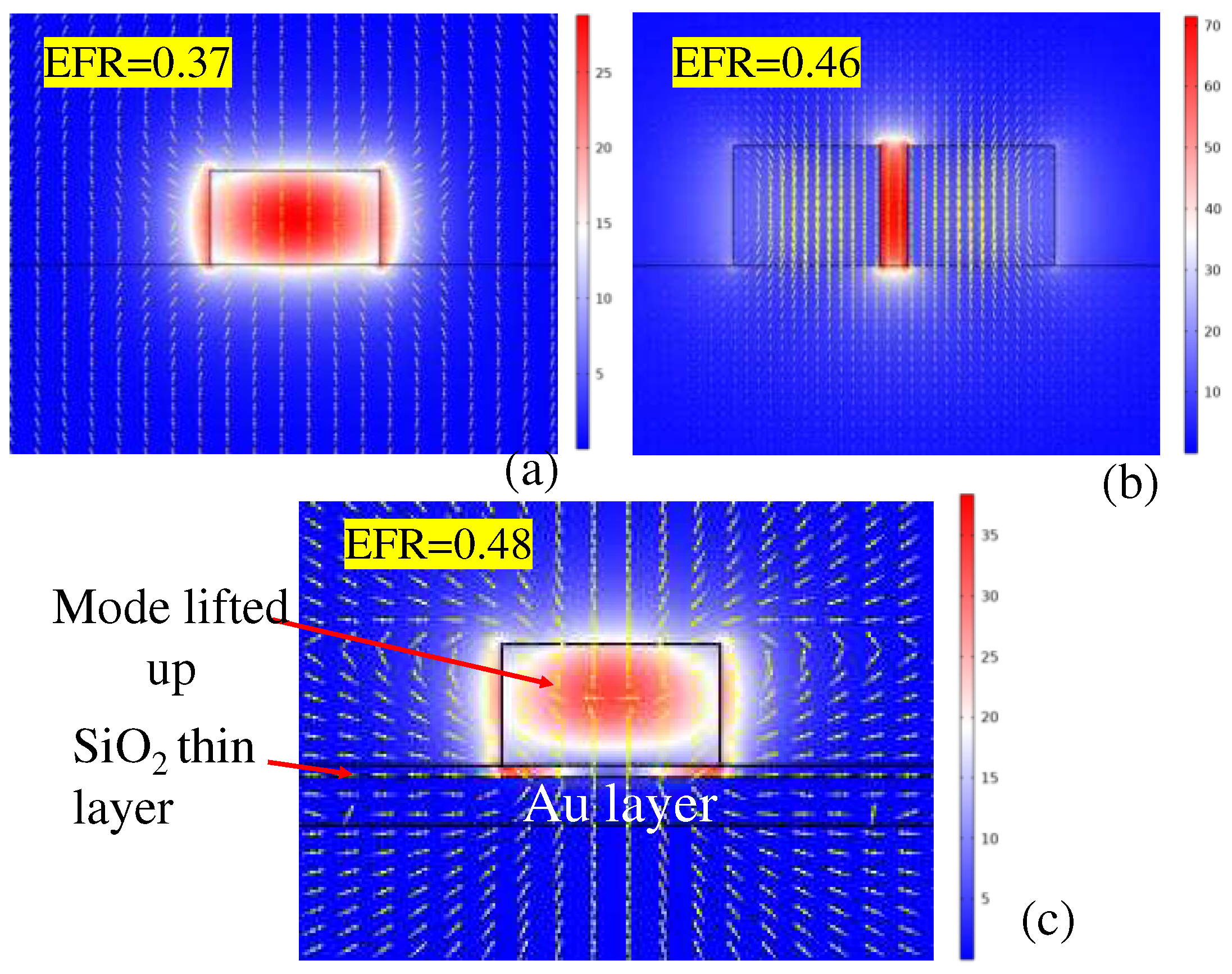
Rib WGs, ridge WGs, and slot WGs are different types of optical WGs, and their properties, including the characteristics of the evanescent field, can vary. Rib WGs typically consist of a thin strip (rib) of high refractive index material on a lower refractive index substrate. The evanescent field in rib WGs is generally confined within the high-index region of the WG. The field extends into the cladding but is typically more localized compared to other types of WGs. Ridge WGs has a raised section (ridge) on the WG core, which helps in confining and guiding light. Like rib WGs, the evanescent field in ridge WGs is primarily localized within the high-index region. The dimensions of the ridge can affect the characteristics of the evanescent field. The normalized E-field distribution in a standard ridge WG determined by finite element method (FEM) is shown in Figure 2a.
Whereas slot WGs consist of a low-index region (slot) between two high-index regions [36]. These WGs are designed to have a substantial part of the optical field concentrated in the low-index slot region as shown in Figure 2b. This design allows for strong light-matter interactions in the slot, making them advantageous for applications such as sensing [4]. While rib and ridge WGs primarily confine the evanescent field within the high-index regions, slot WGs intentionally utilize a low-index slot to enhance the interaction between light and the surrounding medium. The choice of WG depends on the specific requirements of the application, such as the desired level of confinement, interaction strength, and the nature of the surrounding medium.
In [33], Butt et al. proposed a novel metal-assisted silicon strip WG configuration aimed at enhancing the EFR, thereby making it suitable for highly sensitive sensor applications. The metal assisted WG structure incorporates a thin SiO2 layer positioned between the gold layer and the silicon strip WG. The mode in the metal-assisted silicon strip WG is heightened, leading to an approximately 10% increase in power within the upper cladding, while the power in the substrate experiences a reduction of approximately 5%. The normalized E-field distribution in the metal-assisted silicon strip WG is shown in Figure 2c. These results showcase a significant improvement in the evanescent field within the upper cladding region of a straight strip WG, positioning it as an ideal choice for gas absorption sensors relying on evanescent field interactions.
The subwavelength grating (SWG) WG is recognized for its ability to enhance the evanescent field, a crucial feature in various optical applications [37]. By leveraging periodic structures with dimensions smaller than the wavelength of the guided light, subwavelength gratings facilitate strong coupling between guided modes and the surrounding medium. This design leads to a significant increase in the penetration depth of the evanescent field beyond the WG core. The subwavelength grating's unique geometric configuration allows for fine-tuning of the effective refractive index and dispersion characteristics, providing engineers with a versatile tool to tailor the evanescent field's strength and distribution [38]. This enhanced evanescent field is particularly advantageous in applications such as sensing, where interactions with the surrounding environment play a critical role. The subwavelength grating WG's capability to amplify the evanescent field opens up new possibilities for achieving heightened sensitivity and improved performance in optical devices [39,40,41].
Apart from dielectric WGs, there is another type of optical WG that offers a high evanescent field for light-matter interaction is a plasmonic WG [42]. These WGs are designed to guide SPPs, which are collective oscillations of electrons coupled to photons at a metal-dielectric interface. The evanescent field in plasmonic WGs extends into the surrounding medium, allowing for strong light-matter interactions in the adjacent regions. This property is particularly advantageous for applications such as sensing, where the evanescent field can be used to probe changes in the refractive index or absorbance of the surrounding medium. Other types of WGs, such as dielectric or photonic crystal WGs, may also offer high evanescent fields depending on their specific design parameters and configurations [16,43,44]. However, plasmonic WGs are often specifically engineered to enhance the evanescent field and enable efficient light-matter interactions in their vicinity.

4. Choice of a suitable platform for sensing applications

Silicon-On-Insulator (SOI), Silicon Nitride (Si3N4), and polymer materials are three distinct platforms that play crucial roles in the realm of photonic sensors, each offering unique advantages and tailored properties to meet specific sensing requirements [45,46,47,48,49,50]. SOI platforms are characterized by their high refractive index contrast between the silicon WG and the surrounding insulator layer, allowing for efficient light confinement [51]. This enables the creation of compact and low-loss photonic components, such as WGs and resonators, making SOI an excellent choice for integrated photonics. SOI's compatibility with standard silicon processing techniques ensures seamless integration with electronic devices, fostering the development of highly integrated sensor systems.
Si3N4, on the other hand, boasts a wide transparency range and compatibility with CMOS processes, making it well-suited for various photonic applications. Si3N4's transparency in the visible and near-infrared regions is essential for effective light transmission in sensors. Its compatibility with CMOS processes facilitates the integration of electronic and photonic components on a single chip, contributing to the advancement of integrated photonic circuits [48,52].
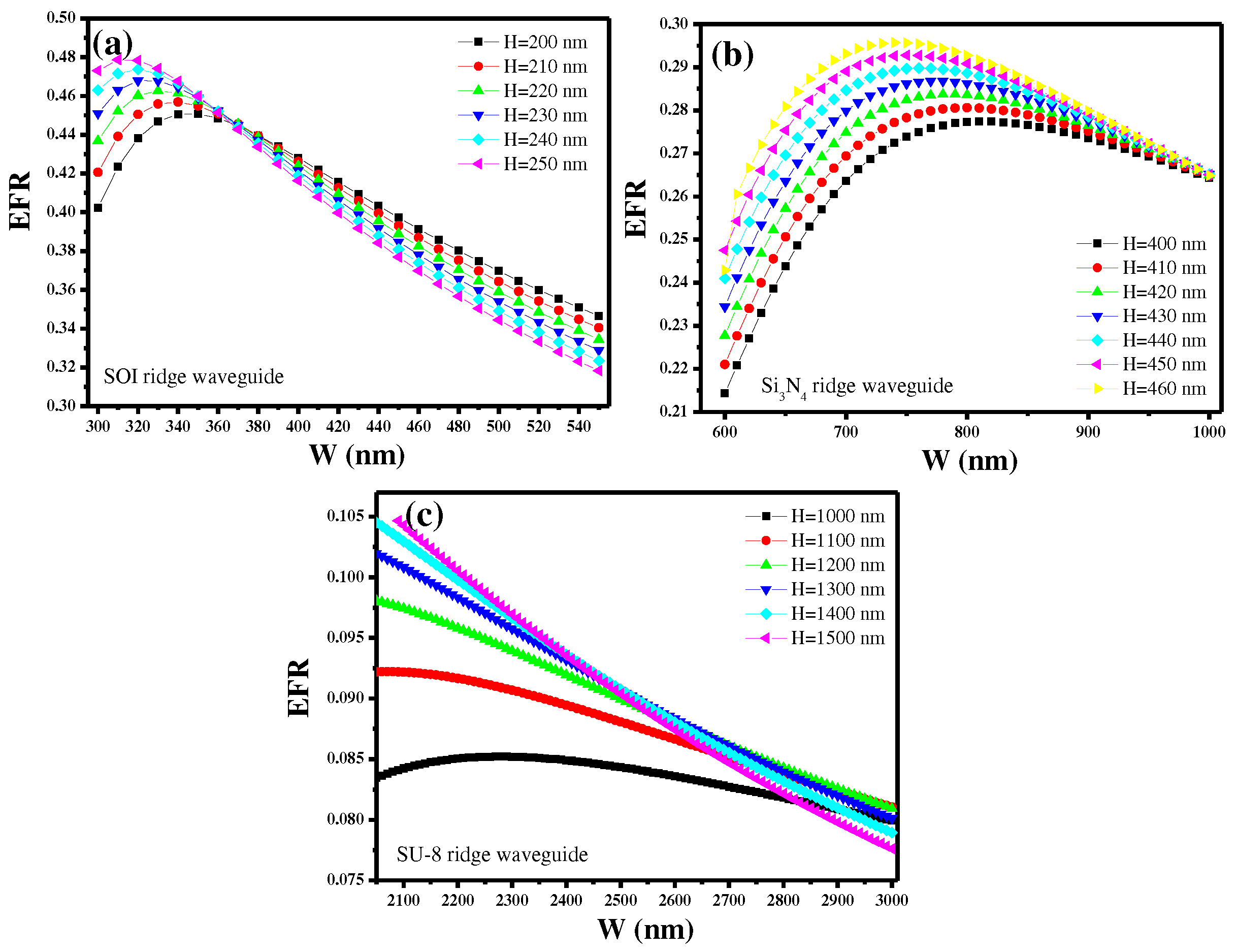
Polymeric materials, such as SU-8 and PDMS, offer a different set of advantages. Their tunable optical and mechanical properties allow for the fabrication of flexible and customizable sensor structures [53]. Polymers are particularly valuable for their ease of fabrication, low cost, and biocompatibility, making them suitable for applications like biosensing [54,55]. The adaptability of polymers to various deposition and patterning techniques further enables scalable and cost-effective manufacturing processes [56]. Figure X illustrates the EFR of ridge WGs based on SOI, Si3N4, and SU-8 polymer materials. The numerical analysis is conducted via FEM. The optimization of WG core dimensions, specifically width (W) and height (H), enhances the EFR values, contributing to superior sensing performance. Observing Figure 3a–c, it is evident that the SOI platform outperforms Si3N4 and SU-8 polymer in terms of EFR. Notably, the SOI-based device exhibits a smaller footprint compared to the other two platforms, underscoring its compact design. This compactness not only contributes to efficient use of space on chips but also emphasizes the potential for highly sensitive photonic sensors based on SOI.
Moreover, the sensitivity of the device can be further enhanced by modifying the WG architecture [57]. The sensitivity of optical WGs varies with their geometry primarily due to differences in the distribution of the optical mode and its interaction with the surrounding medium. The geometry of a WG dictates the confinement and propagation characteristics of the guided optical mode. For instance, in slot WGs, where a low-index region is sandwiched between high-index layers, the optical mode extends into the low-index region, leading to a stronger interaction with changes in the refractive index of the surrounding medium [58,59,60]. On the other hand, WGs with different geometries, such as ridge WGs, may confine the optical mode within a high-index core, limiting its interaction with the external environment. The sensitivity is influenced by the extent to which the optical mode penetrates the surrounding medium, allowing for enhanced detection of changes in refractive index or other environmental parameters. Therefore, the choice of WG geometry plays a crucial role in determining the sensitivity of the WG for specific applications, such as sensing, communication, or signal processing [37].
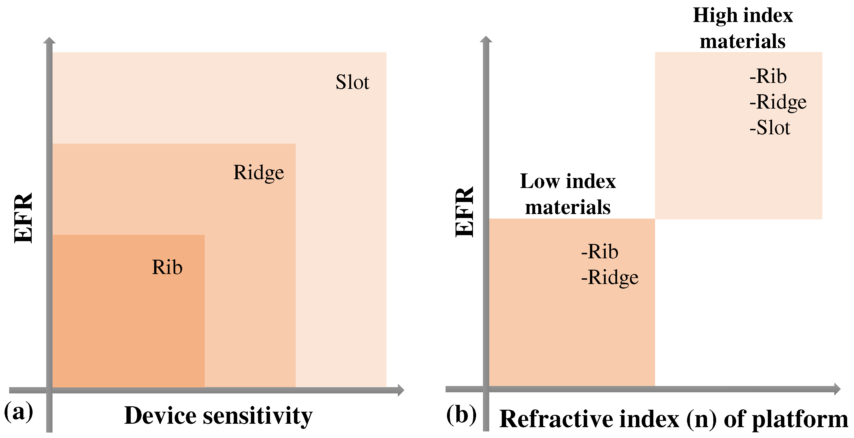
Figure 4a illustrates the correlation between device sensitivity and EFR concerning the optical WG's geometry, including rib, ridge, and slot WG. Notably, the slot WG exhibits superior EFR, thereby leading to heightened device sensitivity. Consequently, it is recommended to produce photonic sensors based on slot WGs for enhanced sensing performance. In Figure 4b, the association between the refractive index of the material platform and EFR is depicted. It is crucial to note that slot WGs cannot be realized using low-index materials like polymers. Consequently, the fabrication of standard WG geometries such as rib and ridge become the feasible option. Additionally, optical platforms capable of providing higher refractive index contrast can be employed to create various WG types, including slot and hybrid configurations. In summary, material platforms featuring high refractive index contrast play a pivotal role in achieving elevated EFR, thereby facilitating the development of highly sensitive devices. It is essential to consider these factors in the design and manufacturing processes of photonic sensors for optimal performance.

5. Applications

Optical WG-based photonic sensors utilizing the evanescent field have found diverse applications across various scientific and technological domains. These sensors leverage the unique property of the evanescent field, a phenomenon where the electromagnetic wave extends beyond the WG's core, interacting with the surrounding medium. In biochemical sensing, these sensors are employed for label-free detection of biomolecules, such as proteins and DNA, enabling real-time monitoring of molecular interactions crucial for medical diagnostics and pharmaceutical research [61]. Environmental monitoring benefits from these sensors by detecting and analyzing pollutants in air or water. The versatility and sensitivity of optical WG sensors utilizing the evanescent field make them invaluable tools across a wide spectrum of scientific and industrial applications [62]. Within this section, our attention is directed towards two prevalent applications of photonic sensors, specifically in the realms of gas sensing and biosensing. Some of the recently proposed photonic devices used for biosensing and temperature sensing are charted in Table 1.

5.1. Evanescent field absorption gas sensors

Gas sensors play a pivotal role in safeguarding human health and the environment by enabling the detection of toxic gases and facilitating environmental monitoring [63,64]. In industrial settings, where various hazardous substances may be present, gas sensors serve as critical tools for early warning and mitigation of potential threats. These sensors can detect the presence of harmful gases, such as carbon monoxide, hydrogen sulfide, or volatile organic compounds, which are often colorless and odorless, posing a significant risk to human health. In environmental monitoring, gas sensors contribute to assessing air quality, tracking pollution levels, and ensuring compliance with regulatory standards [65,66]. The timely and accurate detection of toxic gases allows for swift response measures, helping prevent accidents, minimize exposure, and mitigate environmental damage [67]. Additionally, gas sensors are essential in public spaces, residential areas, and workplaces to create safer and healthier environments. The continuous advancements in gas sensing technologies enhance our ability to monitor and manage air quality, providing valuable data for informed decision-making and contributing to sustainable practices for a cleaner and safer world.
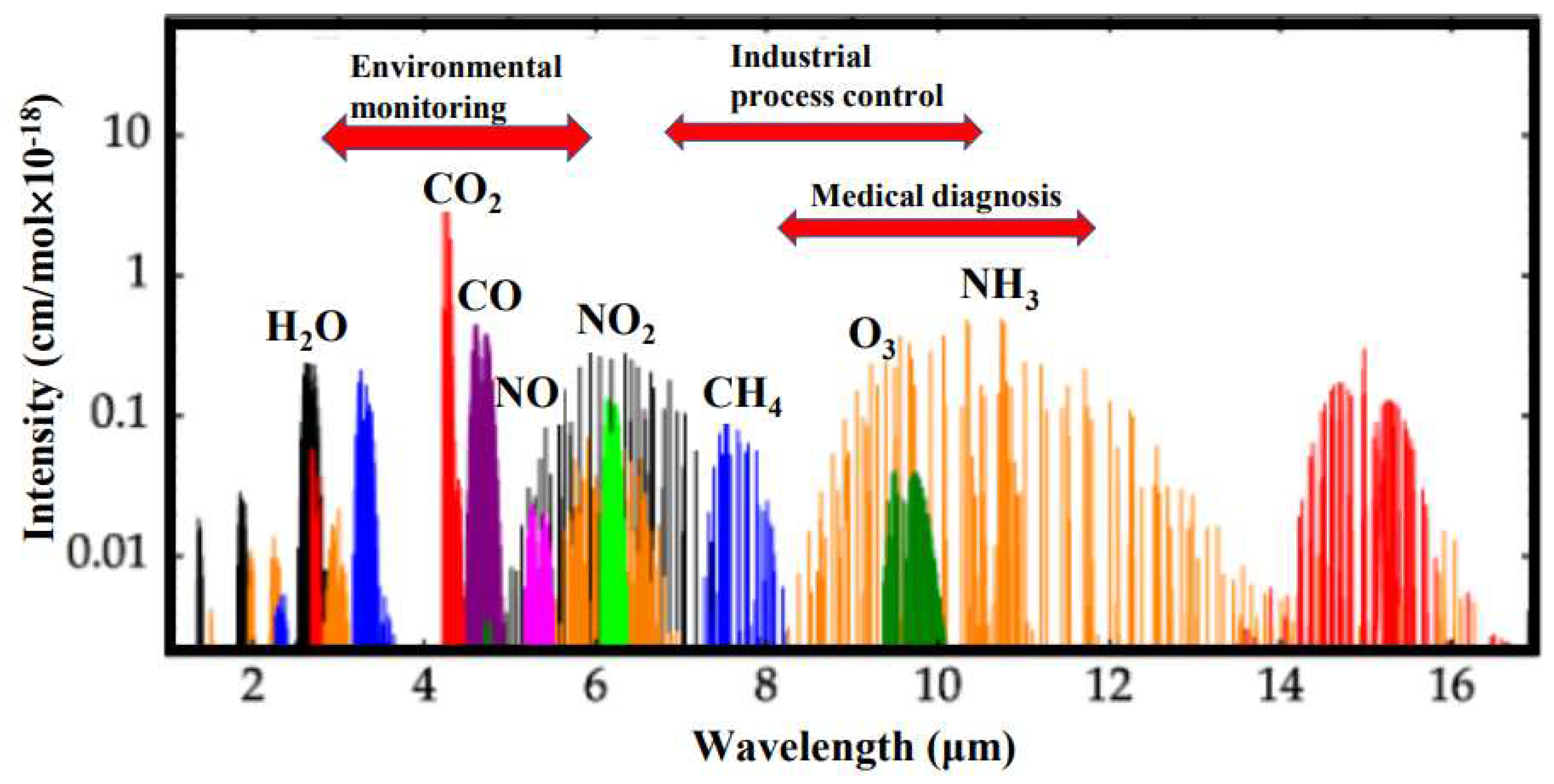
The mid-infrared (MIR) spectrum serves as a crucial domain for gas analysis due to the presence of distinctive absorption lines for various gases. Each gas exhibits unique absorption features at specific wavelengths in the MIR region, creating distinct absorption lines as shown in Figure 5 [68]. These lines result from the vibrational and rotational transitions of gas molecules when exposed to MIR radiation. The ability to identify and analyze these absorption lines enables precise identification and quantification of gases in complex mixtures. This characteristic spectral fingerprinting is particularly valuable in environmental monitoring, industrial process control, and gas sensing applications. For instance, carbon dioxide (CO2), methane (CH4), and water vapor (H2O) each display characteristic absorption lines in the MIR, facilitating their selective detection and measurement. The study and exploitation of absorption lines in the MIR spectrum have become integral to advancing technologies for gas sensing and analysis across a diverse range of scientific and industrial domains [34].
When formulating the integrated photonic sensor, particular attention must be given to a multitude of parameters. These design parameters wield considerable influence, shaping crucial aspects such as sensitivity and dynamic range within the WG sensor. Leading among these considerations is the profound significance of the evanescent field's penetration into the low index/cladding region. This specific measure, denoted as the penetration depth of the evanescent field, stands out as a pivotal factor in the overall efficacy of the sensor design. Understanding and optimizing the penetration depth is paramount for achieving optimal performance and accurate sensing capabilities [69]. Each gas possesses a distinct absorption peak, akin to a unique fingerprint, defining its molecular identity. When the WG sensor is placed in a gaseous environment, constituting the cladding, the evanescent field engages with the gas present. Consequently, the transmitted light undergoes attenuation if its wavelength aligns with the absorption lines of the targeted gas. The extent of attenuation is typically contingent upon both the concentration of the sensing gas and the evanescent field ratio (EFR) of the WG which is defined as the ratio of the evanescent field power in the cladding gas to the total modal power [70]. This interplay forms the basis for discerning and quantifying the presence of specific gases, making the WG sensor a sophisticated tool for gas sensing applications.
The works presented in [5,71] have comprehensively explored the analysis of methane gas sensors based on SOI technology. However, their work highlights a limitation beyond the wavelength of 3.6 μm, where the SiO2 material undergoes high absorption. Consequently, the use of SOI-based WGs in the MIR region becomes impractical. Considering this constraint, alternative materials exhibiting a broad transparency range in the MIR region, as discussed by [72,73,74] emerge as viable candidates. Materials such as Ge and CaF2, characterized by high-index contrast, present promising alternatives for methane gas sensing applications when compared to SOI materials. For a comprehensive understanding of gas sensor analyses for different gases, noteworthy contributions have been made in [75,76]. These studies collectively contribute to the broader landscape of gas sensing technologies, providing valuable insights into the diverse applications and material considerations essential for advancing sensor performance.
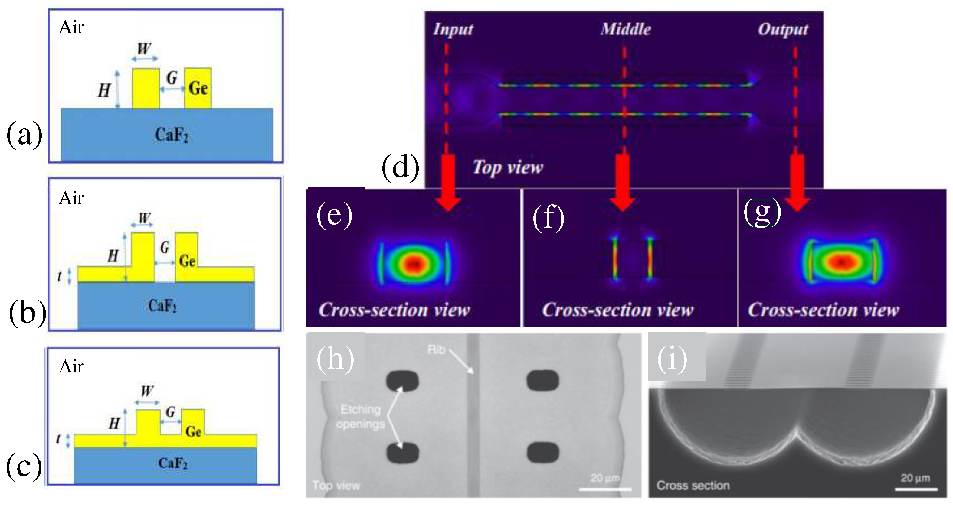
The slot WG has emerged as a promising candidate for designing evanescent field absorption-based photonic gas sensors. In [77], three different slot WG structures—conventional slot, partial-strip-loaded slot, and full-strip-loaded slot are discussed—for analyzing their sensing performance with methane gas as shown in Figure 6a–c. To enhance the EFR in the slot region and consequently improve the gas sensor's capabilities, these slot WG structures are designed by depositing the germanium layer over calcium fluoride in various ways. Simulation results indicate that the full-strip-loaded slot WG outperforms the others, boasting a higher evanescent field (28%) and increased sensitivity (73.76 L/Mol). Following closely is the partial-strip-loaded slot WG, particularly for a target value of propagation loss (3 dB/cm).
Khonina et al. introduced a significant enhancement in EFR of a ridge WG by transforming it into a dual hybrid plasmonic WG [34]. This improvement is achieved through the strategic tapering of the middle section of the WG and the incorporation of a gold layer on both sides, creating a sub-wavelength gap. The optimization of the WG geometry at 3.392 μm, corresponding to an absorption line of methane gas, further adds to the efficacy of the design. This WG scheme not only optimizes the geometry but also provides a spacious WG cross-section, enabling a flexible yet efficient coupling of light with an intensified evanescent field in the middle section. The E-field distribution in the WG is shown in the Figure 6d–g. To validate the findings, the finite element method is employed to analyze various parameters such as the EFR, propagation loss, confinement factor, and electric field distribution of the WG. The results demonstrate an elevated evanescent field ratio of 0.74, coupled with a low propagation loss of approximately 0.7 dB/μm. The sensitivity of the proposed WG scheme is quantified as 0.0715 (mW/gas conc.), determined by calculating the decay in transmission power due to the absorption of gas in the medium. This work presents a promising advancement in the field of plasmonic WGs with practical applications in gas sensing and other related technologies.
Nanophotonic WGs stand as the backbone of an extensive array of optical sensors, confining light within defined paths on photonic chips and facilitating light–matter interaction through evanescent fields. Despite their versatility, WGs have traditionally fallen short in sensitivity-critical applications, such as trace gas detection, when compared to free-space optics. Challenges such as limited optical path lengths, diminished interaction strengths, and unwanted etalon fringes in spectral transmission have impeded the progress of on-chip gas sensing, keeping it in its emerging stages. In [3], a significant leap forward in the realm of integrated WG sensors is demonstrated, particularly in the MIR range, effectively overcoming these challenges. The microscope image and SEM image of the freestanding shallow rid WG are shown in Figure 6h,i, respectively. The sensor showcased in this work achieves an impressive 107% evanescent field confinement factor in air. This not only matches but surpasses the performance of free-space beams, especially in terms of per-length optical interaction. Notably, the mitigation of facet reflections contributes to a remarkably flat spectral background, resulting in a record-low level of absorbance noise. This breakthrough allows the on-chip sensor to finally rival the precision of free-space spectroscopy. The sensor's capabilities were rigorously validated at a wavelength of 2.566 μm, demonstrating a remarkable 7 ppm limit of detection (LOD) for acetylene with a mere 2 cm long WG. This advancement not only enhances the feasibility of on-chip gas sensing but also positions integrated WG sensors as formidable contenders in high-sensitivity applications traditionally dominated by free-space optics.

5.2. Biosensing applications

Photonic devices play a pivotal role in advancing biosensing applications, offering a myriad of advantages that significantly enhance the capabilities of biological detection and analysis [1]. The use of light-based technologies enables highly sensitive and rapid detection of biological molecules, such as proteins, nucleic acids, and pathogens. Photonic biosensors leverage the interaction of light with biomolecules, allowing for precise and label-free detection, which is crucial for preserving the integrity of biological samples. Moreover, the versatility of photonic devices facilitates the development of miniaturized and portable biosensors, enabling point-of-care diagnostics and real-time monitoring [78]. These devices contribute to the early detection of diseases, biomarker analysis, and environmental monitoring, fostering advancements in personalized medicine and public health [79]. The integration of photonics with biosensing not only enhances sensitivity and specificity but also opens avenues for innovative and interdisciplinary research, paving the way for novel diagnostic tools with broad applications in healthcare, biotechnology, and beyond.
MRRs stand as pivotal elements within the realm of integrated optics, belonging to the class of common refractive index sensors [33,80]. They offer a myriad of advantages, including a high Q-factor, straightforward preparation, and ease of mass production. Consequently, MRRs find extensive application not only in the sensor domain but also in fields like lasers and detectors. Enhancing the sensor LOD can be achieved through two principal approaches [81,82]. Firstly, the Q-factor of the resonator can be optimized to minimize the impact of noise on the measurement of the resonance wavelength. Secondly, maximizing the mean resonance wavelength shift is attainable by enhancing the interaction between light and biomolecules affixed to the WG surface [83,84].
MRRs have garnered significant attention as silicon photonic biosensors due to their straightforward design and easy fabrication process. The Genalyte platform, a commercially available silicon photonic biosensing system, employs ring resonators for TE polarized light. This configuration offers a bulk sensitivity of 54 nm/RIU and a detection limit of 1 ng/mL, or 10−5 RIU [81]. However, many clinical diagnostic assays demand even lower LODs, necessitating secondary amplification [85]. The key to achieving clinically relevant sensitivities lies in robust surface chemistries that resist fouling, allowing high densities of capture molecules, coupled with optimal sensor performance. Consequently, various research groups have endeavoured to enhance the sensitivity of MRRs.
The sensitivity of these sensors is governed by the overlay of the E-field with the analyte, which can be enhanced by increasing this overlap [86]. Given the high index contrast of Si/SiO2 most of the E-field is narrowed to the core of the WG for TE polarized light. One approach to boosting sensitivity for TE light is to reduce the WG thickness, as determined by Talebi Fard et al. with a 90 nm thick WG achieving a bulk sensitivity of 100 nm/RIU [87]. European collaborative biosensing projects such as SABIO and InTopSens have explored the use of TE polarized slot WGs [88,89], achieving sensitivities of 212 nm/RIU and 298 nm/RIU, respectively [90,91], with LODs on the order of 5×10⁻⁶ RIU. In a comparable WG geometry, the confinement of TM polarized light is weaker, resulting in improved sensitivities to 200 nm/RIU [92].
Finally, a slot WG Bragg grating with a sensitivity of 340 nm/RIU is determined by [93]. These advancements underscore the continuous efforts to refine silicon photonic biosensors, particularly ring resonators, to meet the demanding requirements of clinical diagnostic assays. The methodology for tailoring the effective refractive index and mode profile of a SOI WG by leveraging the capabilities of sub-wavelength gratings (SWG) is presented in [94]. The focus centers on the application of this engineered WG as a biosensor. To realize this design, a 30 μm diameter SWG RR was meticulously crafted, employing state-of-the-art E-beam lithography for fabrication. Upon comprehensive characterization, this engineered SWG RR exhibited a notable Q-factor, reaching 7×10³. The bulk sensitivity was measured at 490 nm/RIU, highlighting the device's precision in detecting changes in refractive index. The system's limit of detection, LOD, was determined to be 2×10⁻⁶ RIU, underscoring the device's remarkable sensitivity.
The landscape of materials employed in integrated optics has evolved significantly, driven by the emergence of innovative materials such as SiO2, LiNbO3, SOI, GaAs, InP, and organic polymers [10,38]. SOI-based optical WG systems boast several advantages, including a substantial refractive index difference, minimal transmission loss, and a high degree of integration capability. This diversification in materials contributes to the versatility and efficiency of integrated optics, expanding its applications across various technological domains.
MZI-structured sensors represent a prevalent category of label-free optical sensing devices known for their simplicity, seamless integration capabilities, and compatibility with special materials or other flexible optical devices. With a LOD typically falling between 105 RIU and 107 RIU, these sensors offer advantages such as high refractive index sensitivity, robust anti-interference capabilities, and efficient detection, making them of significant research interest and practical value in the realm of biochemical sensing. Optical WG sensors, encompassing variations like optical WG temperature sensors, stress sensors, and various biochemical sensors, have become global research focal points. Notably, investigations into optical WG biochemical sensors have predominantly centered on SPR and WG grating sensors. While these sensors boast high sensitivity and rapid response recovery, they often struggle with poor selectivity and weak anti-interference capabilities. In contrast, MZI optical WG sensors emerge as compelling alternatives, offering heightened sensitivity, robust selectivity, anti-interference prowess, and compact dimensions.
As per existing reports, the MZI optical WG sensor achieves an impressive phase-difference resolution of 5×10−5 × 2π, with a refractive index change resolution of approximately 2 × 10⁻⁸. The sensor attains a detection capability for specific analytes at concentrations as low as 10−6 [18]. Furthermore, stringent requirements mandate that the transmission loss of the optical WG remains below 1 dB. In the realm of WG-based sensors for optical signal readout, both MRRs and MZIs are widely adopted configurations [95]. MRR biochemical sensors excel in detecting proteins, DNA, viruses, and bacteria due to their heightened sensitivity. However, their reliance on wavelength-tunable lasers and spectral analyzers for wavelength scanning limits their detection capabilities, constrained by the resolution of costly and complex external devices. In contrast, the MZI readout configuration relies on light intensity detection, eliminating the need for tunable lasers or optical spectrum analyzers [96]. This characteristic makes the miniaturization and integration of an optical WG MZI as a sensing platform system not only feasible but also advantageous [59].
Traditional MZI sensors employing intensity interrogation demand highly sensitive power sensors and exceptionally stable systems to achieve the desired low noise levels and heightened sensitivity. While sensors with RR structures can address this challenge by precisely determining wavelength shifts, they necessitate a high-resolution spectrometer. To enhance sensitivity, some sensors utilize the Vernier effect, particularly those based on two cascaded RRs. However, the remarkable sensitivity achieved through a significantly large Vernier factor comes with certain drawbacks. A breakthrough in this domain was achieved by Jiang et al. [97], who developed ultra-high-sensitivity silicon photonic biosensors using cascaded MZIs and RRs with the Vernier effect. Remarkably, the sensitivities attained for MZI and MZI ring sensors were as impressive as 2870 and 21,500 nm/RIU, respectively. The application of these sensors in biosensing was exemplified by monitoring the interaction between goat and anti-goat immunoglobulin G (IgG). The measurement results showcased that a concentration as low as 1 ng/mL of IgG led to wavelength shifts of 0.035 nm and 0.5 nm for the MZI and MZI ring sensors, respectively. To assess the reliability of these sensors, the measured temperature drifts were found to be 76 pm/°C for MZI sensors and 271 pm/°C for MZI ring sensors. Despite the higher sensitivity of MZI ring-based sensors, the results suggest that both types of sensors hold promise for deployment in medical diagnosis, demonstrating their potential to deliver highly sensitive and accurate measurements in relevant applications.
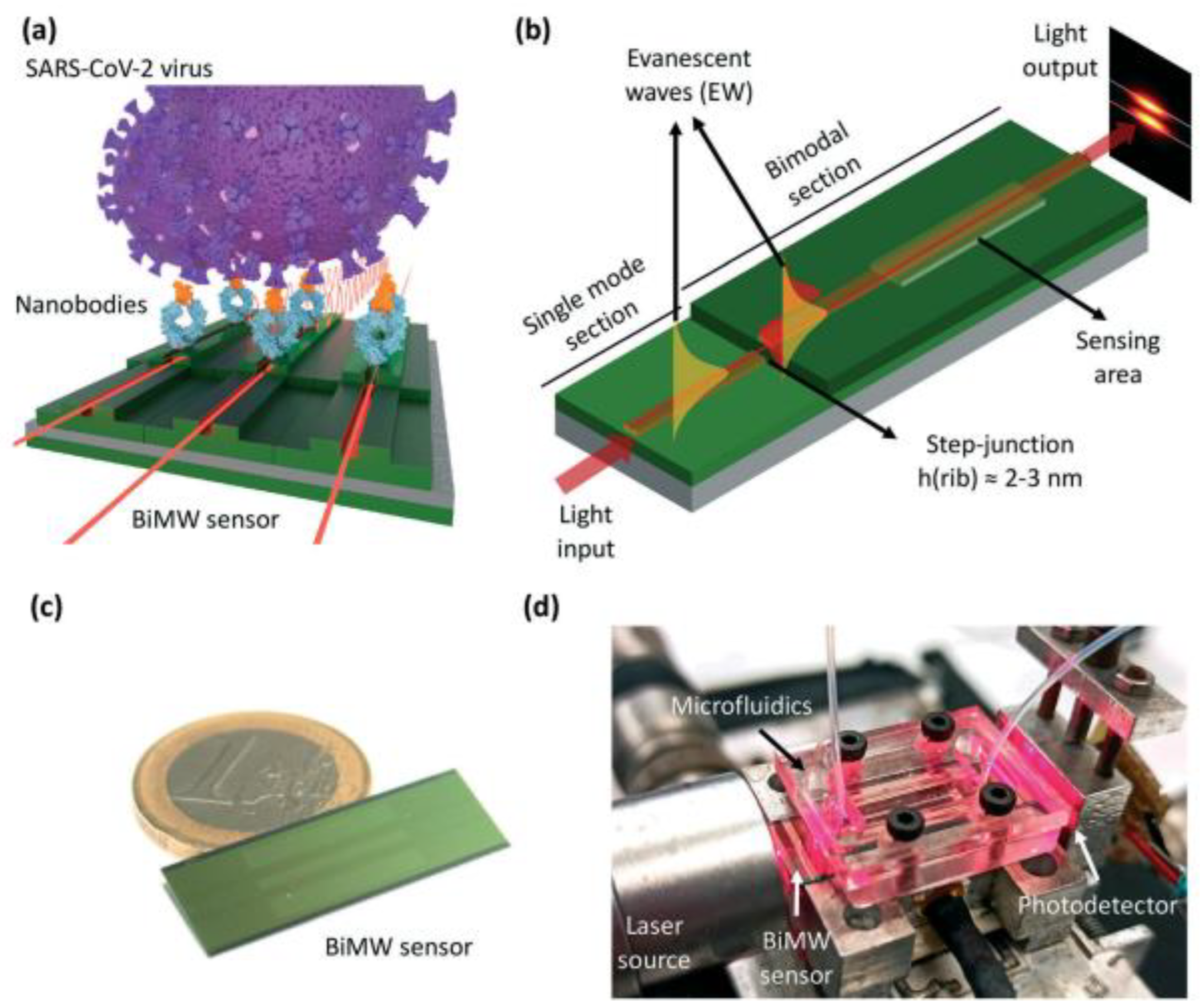
COVID-19 is anticipated to persist as an endemic disease in the years to come, necessitating global readiness to effectively handle the highly contagious SARS-CoV-2. Swift and early identification of SARS-CoV-2 infection is essential for disease control, disrupting transmission, and ensuring timely medical intervention. An innovative nanophotonic biosensor designed for the quantitative detection of viral particles in under 20 minutes is presented in [98] as shown in Figure 7a. The establishment of a step junction leads to the formation of two distinct regions. Initially, the junction permits the propagation of the fundamental mode, characterized by a WG core thickness of 150 nm. Subsequently, in the second section, both the fundamental and first-order modes can propagate, with a WG core thickness increased to 340 nm (refer to Figure 7b). The photonic chip, measuring 1 cm in width and 3 cm in length, is equipped with an array of 20 individual straight rib WGs, each having a rib height ranging from 1 to 3 nm (refer to Figure 7c). The BiMW interferometric biosensor system utilizes a low-power polarized laser diode operating at a visible wavelength (λ = 660 nm, P = 120 mW) as the light source. This laser is coupled into the rib WG, while a two-sectional photodiode serves as the detector for reading the interferometric signal (see Figure 7d) [98].
This nanosensor, utilizing bimodal WG (BiMW) interferometric technology, is equipped with novel bioengineered nanobodies (Nb) that specifically target the receptor-binding domain (RBD) of SARS-CoV-2. This methodology involves the direct capture of viral particles, enabling the detection of the SARS-CoV-2 virus with remarkable sensitivity, reaching below 200 TCID50 per mL. It offers accurate viral load determination across a wide dynamic range (102 – 106 TCID50 per mL). Both the nanobodies and the sensor nanotechnology can be produced on a large scale through highly efficient and cost-effective procedures. They are seamlessly integrated into a user-friendly point-of-care device for decentralized and multiplexed operation. Implementing this unique biosensor in primary care, hospitals, pharmacies, or private laboratories holds the potential to significantly alleviate the burden on healthcare systems and enhance the clinical and social management of COVID-19 [98].
Table 1. Recent photonic devices for gas sensing and biosensing applications utilizing evanescent field.
Device type Platform Application Sensitivity Reference
Ridge WG Silicon-on-insulator Gas sensing - [99]
Slot WG and Subwavelength grating slot WG Silicon-on-insulator Gas sensing
I)
6.66 ×10⁻⁵ (ppm-1)
II)
2.60 ×10⁻⁵ (ppm-1)
[100]
Double slot WG based MZI Polymer Biosensing 2.39 ×10⁵ nm/RIU [101]
Slot WG Si3N4 Biosensing 212 nm/RIU [102]
Rib WG Silicon-on-sapphire Gas sensing - [70]
Modified ridge WG Silicon-on-insulator Gas sensing 0.0175 mW/gas conc. [34]
Horizontal slot WG Silicon-on-insulator Biosensing 893.5 nm/RIU [103]
Hybrid plasmonic WG-based ring resonator Silicon-on-insulator Biosensing 580 nm/RIU [104]
Hybrid plasmonic WG-based ring resonator Silicon-on-insulator
I)
Gas sensing;
II)
Biosensing
I)
690 nm/RIU;
II)
401 nm/RIU
[84]
Double slot hybrid plasmonic WG based MZI structure Silicon-on-insulator Biosensing 1061 nm/RIU [105]
Racetrack ring resonator Silica-titania Biosensing 142.5 nm/RIU [11]
Subwavelength grating structure Silica-titania Biosensing 120 nm/RIU [41]
Planar optical WG Polymer Biosensing 0.75 pixel/nM [106]
SWG hybrid plasmonic WG SOI Biosensing 1000 nm/RIU [107]
Plasmonic WG loaded with functional polymer Gold Gas sensing 226 pm/ppm [108]
Polymer WG coupled surface plasmon Polymer Biosensing 4518.14 nm/RIU [109]

6. Conclusions

Utilizing the evanescent field, photonic sensors provide a sophisticated means of detecting and analyzing diverse substances with exceptional sensitivity. These sensors capitalize on the distinct properties of the evanescent field—an electromagnetic field extending just beyond the surface of an optical WG. As light traverses the WG, a portion of its energy infiltrates the surrounding medium, giving rise to the evanescent field. Photonic sensors exploit variations in this field induced by the presence of specific target substances, including biological molecules or chemical analytes. Interactions between these substances and the evanescent field lead to changes in the field's intensity or phase, facilitating precise measurements. Particularly beneficial in biosensing applications, this approach enables label-free detection and real-time monitoring of biomolecular interactions. Evanescent field-based photonic sensors find diverse applications in medical diagnostics, environmental monitoring, and industrial processes, underscoring their versatility and significant potential across multiple fields. Ridge WGs, slot WGs, and hybrid plasmonic WGs each present unique sensitivities in the realm of photonic sensors. Slot WGs offer enhanced sensitivity by leveraging the subwavelength gap between two closely spaced layers, facilitating strong light-matter interactions. Hybrid plasmonic WGs, combining dielectric and plasmonic materials, exhibit heightened sensitivity owing to the surface plasmon resonance effect, amplifying the electromagnetic field at the WG surface. The choice between these WG configurations depends on specific application requirements and the nature of the target analytes, with each design offering a tailored balance between sensitivity, fabrication complexity, and integration capabilities in the context of photonic sensing technologies. This review provides a brief overview of the integrated photonic sensors realized for biosensing and gas sensing applications.

Author Contributions

Conceptualization, M.A.B.; methodology, M.A.B.; software, M.A.B.; validation, M.A.B.; formal analysis, M.A.B.; investigation, M.A.B.; resources, M.A.B.; data curation, M.A.B.; writing—original draft preparation, M.A.B.; writing—review and editing, M.A.B.; visualization, M.A.B.; supervision, M.A.B.; project administration, M.A.B.; funding acquisition, M.A.B. All authors have read and agreed to the published version of the manuscript.

Funding

This research received no external funding.

Data Availability Statement

Not applicable.

Acknowledgments

The author acknowledges the constant support of Warsaw University of Technology, Poland for the completion of this work.

Conflicts of Interest

The authors declare no conflicts of interest.

References

  1. M. A. Butt, N. L. Kazanskiy, S. N. Khonina, G. S. Voronkov, E. P. Grakhova, and R. V. Kutluyarov, ‘A Review on Photonic Sensing Technologies: Status and Outlook’, Biosensors, vol. 13, no. 5, Art. no. 5, May 2023. [CrossRef]
  2. S. Ghosh, T. Dar, C. Viphavakit, C. Pan, N. Kejalakshmy, and B. M. A. Rahman, ‘Compact Photonic SOI Sensors’, in Computational Photonic Sensors, M. F. O. Hameed and S. Obayya, Eds., Cham: Springer International Publishing, 2019, pp. 343–383. [CrossRef]
  3. M. Vlk et al., ‘Extraordinary evanescent field confinement waveguide sensor for mid-infrared trace gas spectroscopy’, Light Sci. Appl., vol. 10, no. 1, Art. no. 1, Jan. 2021. [CrossRef]
  4. M. A. Butt and R. Piramidowicz, ‘Standard slot waveguide and double hybrid plasmonic waveguide configurations for enhanced evanescent field absorption methane gas sensing’, Photonics Lett. Pol., vol. 14, no. 1, Art. no. 1, Mar. 2022. [CrossRef]
  5. M. A. Butt, S. A. Degtyarev, S. N. Khonina, and N. L. Kazanskiy, ‘An evanescent field absorption gas sensor at mid-IR 3.39 μm wavelength’, J. Mod. Opt., vol. 64, no. 18, pp. 1892–1897, Oct. 2017. [CrossRef]
  6. H. Tai, H. Tanaka, and T. Yoshino, ‘Fiber-optic evanescent-wave methane-gas sensor using optical absorption for the 3.392-μm line of a He–Ne laser’, Opt. Lett., vol. 12, no. 6, pp. 437–439, Jun. 1987. [CrossRef]
  7. M. A. Butt, N. L. Kazanskiy, and S. N. Khonina, ‘Tapered waveguide mode converters for metal-insulator-metal waveguide plasmonic sensors’, Measurement, vol. 211, p. 112601, Apr. 2023. [CrossRef]
  8. C. Liu et al., ‘Surface plasmon resonance (SPR) infrared sensor based on D-shape photonic crystal fibers with ITO coatings’, Opt. Commun., vol. 464, p. 125496, Jun. 2020. [CrossRef]
  9. S. Singh, B. Chaudhary, A. Upadhyay, D. Sharma, N. Ayyanar, and S. A. Taya, ‘A review on various sensing prospects of SPR based photonic crystal fibers’, Photonics Nanostructures - Fundam. Appl., vol. 54, p. 101119, May 2023. [CrossRef]
  10. N. L. Kazanskiy, S. N. Khonina, and M. A. Butt, ‘A Review of Photonic Sensors Based on Ring Resonator Structures: Three Widely Used Platforms and Implications of Sensing Applications’, Micromachines, vol. 14, no. 5, Art. no. 5, May 2023. [CrossRef]
  11. M. A. Butt, M. Shahbaz, and R. Piramidowicz, ‘Racetrack Ring Resonator Integrated with Multimode Interferometer Structure Based on Low-Cost Silica–Titania Platform for Refractive Index Sensing Application’, Photonics, vol. 10, no. 9, Art. no. 9, Sep. 2023. [CrossRef]
  12. ‘Waveguide Mach-Zehnder biosensor with laser diode pumped integrated single-mode silicon nitride organic hybrid solid-state laser - ScienceDirect’. Accessed: Jan. 26, 2024. [Online]. Available: https://www.sciencedirect.com/science/article/pii/S0956566321008538.
  13. K. R. Kribich et al., ‘Novel chemical sensor/biosensor platform based on optical multimode interference (MMI) couplers’, Sens. Actuators B Chem., vol. 107, no. 1, pp. 188–192, May 2005. [CrossRef]
  14. ‘Sensors | Free Full-Text | Integrated Lab-on-a-Chip Optical Biosensor Using Ultrathin Silicon Waveguide SOI MMI Device’. Accessed: Jan. 26, 2024. [Online]. Available: https://www.mdpi.com/1424-8220/20/17/4955.
  15. ‘Biosensors | Free Full-Text | A Fiber Bragg Grating Sensor Based on Cladding Mode Resonance for Label-Free Biosensing’. Accessed: Jan. 26, 2024. [Online]. Available: https://www.mdpi.com/2079-6374/13/1/97.
  16. D. Gowdhami, V. R. Balaji, M. Murugan, S. Robinson, and G. Hegde, ‘Photonic crystal based biosensors: an overview’, ISSS J. Micro Smart Syst., vol. 11, no. 1, pp. 147–167, Jun. 2022. [CrossRef]
  17. ‘Biosensors | Free Full-Text | Silicon Integrated Dual-Mode Interferometer with Differential Outputs’. Accessed: Jan. 26, 2024. [Online]. Available: https://www.mdpi.com/2079-6374/7/3/37.
  18. C. Peng et al., ‘Optical Waveguide Refractive Index Sensor for Biochemical Sensing’, Appl. Sci., vol. 13, no. 6, Art. no. 6, Jan. 2023. [CrossRef]
  19. Y. H. Isayama, ‘Design and numerical demonstration of a multimode interference sensor using engineered slot-waveguides’, Opt. Quantum Electron., vol. 56, no. 3, p. 304, Dec. 2023. [CrossRef]
  20. K. Li, S. Li, Z. Yin, and J. Li, ‘Experimental study of SPR sensor performance enhancement by metal oxides’, Infrared Phys. Technol., vol. 136, p. 105021, Jan. 2024. [CrossRef]
  21. ‘Modeling of Mach-Zehnder Interferometric Sensors Employing Ring-Resonator Circuits for Slow-Light Enhancement | IEEE Journals & Magazine | IEEE Xplore’. Accessed: Feb. 04, 2024. [Online]. Available: https://ieeexplore.ieee.org/document/10313014.
  22. Abdalwareth, G. Flachenecker, M. Angelmahr, and W. Schade, ‘Optical fiber evanescent hydrogen sensor based on palladium nanoparticles coated Bragg gratings’, Sens. Actuators Phys., vol. 361, p. 114594, Oct. 2023. [CrossRef]
  23. M. Londero, M. Delgado-Pinar, C. Cuadrado-Laborde, and M. V. Andrés, ‘Resonant Couplings in U-Shaped Fibers for Biosensing’, J. Light. Technol., vol. 41, no. 13, pp. 4230–4237, Jul. 2023. [CrossRef]
  24. S. Shafaay, S. Mohamed, and M. Swillam, ‘Mid-Infrared Gas Sensing Based on Electromagnetically Induced Transparency in Coupled Plasmonic Resonators’, Sensors, vol. 23, no. 22, Art. no. 22, Jan. 2023. [CrossRef]
  25. B. Wang et al., ‘On-Chip Fluorescent Sensor for Chemical Vapor Detection’, Adv. Mater. Technol., vol. 8, no. 19, p. 2300609, 2023. [CrossRef]
  26. T. Tian et al., ‘Sensitivity-Enhanced and Compact Refractometer Based on Double Assembled Long-Period Fiber Gratings With Tapered Fiber Structure’, IEEE Sens. J., vol. 23, no. 18, pp. 21279–21284, Sep. 2023. [CrossRef]
  27. Y. Zhu et al., ‘Microfiber evanescent-field photothermal gas detection using acoustic-induced mode-dependent frequency shift’, Nanophotonics, vol. 12, no. 16, pp. 3229–3242, Aug. 2023. [CrossRef]
  28. J. Canning, W. Padden, D. Boskovic, M. Naqshbandi, H. de Bruyn, and M. J. Crossley, ‘Manipulating and controlling the evanescent field within optical waveguides using high index nanolayers [Invited]’, Opt. Mater. Express, vol. 1, no. 2, pp. 192–200, Jun. 2011. [CrossRef]
  29. C. Consani, C. Ranacher, A. Tortschanoff, T. Grille, P. Irsigler, and B. Jakoby, ‘Evanescent-Wave Gas Sensing Using an Integrated Thermal Light Source’, Proceedings, vol. 1, no. 4, Art. no. 4, 2017. [CrossRef]
  30. N. Punjabi, J. Satija, and S. Mukherji, ‘Evanescent Wave Absorption Based Fiber-Optic Sensor - Cascading of Bend and Tapered Geometry for Enhanced Sensitivity’, in Sensing Technology: Current Status and Future Trends III, A. Mason, S. C. Mukhopadhyay, and K. P. Jayasundera, Eds., in Smart Sensors, Measurement and Instrumentation. , Cham: Springer International Publishing, 2015, pp. 25–45. [CrossRef]
  31. ‘Sensors | Free Full-Text | Evanescent field Sensors Based on Tantalum Pentoxide Waveguides – A Review’. Accessed: Feb. 04, 2024. [Online]. Available: https://www.mdpi.com/1424-8220/8/2/711.
  32. S. Kumar, A. Kumari, and B. Pradhan, ‘Analysis of evanescent field of TE and TM mode in the grounded slab metamaterial waveguide structure’, Optik, vol. 126, no. 23, pp. 3706–3712, Dec. 2015. [CrossRef]
  33. M. A. Butt, S. N. Khonina, and N. L. Kazanskiy, ‘Enhancement of evanescent field ratio in a silicon strip waveguide by incorporating a thin metal film’, Laser Phys., vol. 29, no. 7, p. 076202, May 2019. [CrossRef]
  34. S. N. Khonina, N. L. Kazanskiy, and M. A. Butt, ‘Evanescent Field Ratio Enhancement of a Modified Ridge Waveguide Structure for Methane Gas Sensing Application’, IEEE Sens. J., vol. 20, no. 15, pp. 8469–8476, Aug. 2020. [CrossRef]
  35. C. Consani, F. Dubois, and G. Auböck, ‘Figures of merit for mid-IR evanescent-wave absorption sensors and their simulation by FEM methods’, Opt. Express, vol. 29, no. 7, pp. 9723–9736, Mar. 2021. [CrossRef]
  36. C. Ranacher, C. Consani, R. Jannesari, T. Grille, and B. Jakoby, ‘Numerical Investigations of Infrared Slot Waveguides for Gas Sensing’, Proceedings, vol. 2, no. 13, Art. no. 13, 2018. [CrossRef]
  37. L. Torrijos-Morán, A. Griol, and J. García-Rupérez, ‘Experimental study of subwavelength grating bimodal waveguides as ultrasensitive interferometric sensors’, Opt. Lett., vol. 44, no. 19, pp. 4702–4705, Oct. 2019. [CrossRef]
  38. N. L. Kazanskiy, S. N. Khonina, and M. A. Butt, ‘Subwavelength Grating Double Slot Waveguide Racetrack Ring Resonator for Refractive Index Sensing Application’, Sensors, vol. 20, no. 12, Art. no. 12, Jan. 2020. [CrossRef]
  39. Y. Sun, G. Hu, and Y. Cui, ‘Subwavelength grating waveguide racetrack-based refractive index sensor with improved figure of merit’, Appl. Opt., vol. 59, no. 33, pp. 10613–10617, Nov. 2020. [CrossRef]
  40. K. Awasthi, N. Malviya, and A. Kumar, ‘Silicon Subwavelength Grating Slot Waveguide based Optical Sensor for Label Free Detection of Fluoride Ion in Water’, IETE Tech. Rev., vol. 0, no. 0, pp. 1–12, 2023. [CrossRef]
  41. M. A. Butt, C. Tyszkiewicz, K. Wojtasik, P. Karasiński, A. Kaźmierczak, and R. Piramidowicz, ‘Subwavelength Grating Waveguide Structures Proposed on the Low-Cost Silica–Titania Platform for Optical Filtering and Refractive Index Sensing Applications’, Int. J. Mol. Sci., vol. 23, no. 12, Art. no. 12, Jan. 2022. [CrossRef]
  42. N. L. Kazanskiy, S. N. Khonina, and M. A. Butt, ‘Plasmonic sensors based on Metal-insulator-metal waveguides for refractive index sensing applications: A brief review’, Phys. E Low-Dimens. Syst. Nanostructures, vol. 117, p. 113798, Mar. 2020. [CrossRef]
  43. M. G. Scullion, A. Di Falco, and T. F. Krauss, ‘Slotted photonic crystal cavities with integrated microfluidics for biosensing applications’, Biosens. Bioelectron., vol. 27, no. 1, pp. 101–105, Sep. 2011. [CrossRef]
  44. M. A. Butt, S. N. Khonina, and N. L. Kazanskiy, ‘Recent advances in photonic crystal optical devices: A review’, Opt. Laser Technol., vol. 142, p. 107265, Oct. 2021. [CrossRef]
  45. M. A. Butt, ‘Integrated Optics: Platforms and Fabrication Methods’, Encyclopedia, vol. 3, no. 3, Art. no. 3, Sep. 2023. [CrossRef]
  46. S. Itabashi et al., ‘Silicon Photonics Devices Based on SOI Structures’, ECS Trans., vol. 35, no. 5, p. 227, Apr. 2011. [CrossRef]
  47. D. J. Blumenthal, R. Heideman, D. Geuzebroek, A. Leinse, and C. Roeloffzen, ‘Silicon Nitride in Silicon Photonics’, Proc. IEEE, vol. 106, no. 12, pp. 2209–2231, Dec. 2018. [CrossRef]
  48. Hermans, M. V. Daele, J. Dendooven, S. Clemmen, C. Detavernier, and R. Baets, ‘Integrated silicon nitride electro-optic modulators with atomic layer deposited overlays’, Opt. Lett., vol. 44, no. 5, pp. 1112–1115, Mar. 2019. [CrossRef]
  49. S. M. Garner et al., ‘Three-dimensional integrated optics using polymers’, IEEE J. Quantum Electron., vol. 35, no. 8, pp. 1146–1155, Aug. 1999. [CrossRef]
  50. J. I. Frish et al., ‘Rapid photolithographic fabrication of high density optical interconnects using refractive index contrast polymers’, Opt. Mater. Express, vol. 12, no. 5, pp. 1932–1944, May 2022. [CrossRef]
  51. M. Nedeljkovic et al., ‘Silicon photonic devices and platforms for the mid-infrared’, Opt. Mater. Express, vol. 3, no. 9, pp. 1205–1214, Sep. 2013. [CrossRef]
  52. ‘Integrated Bragg waveguides as an efficient optical notch filter on silicon nitride platform - IOPscience’. Accessed: Dec. 03, 2023. [Online]. Available: https://iopscience.iop.org/article/10.1088/1742-6596/917/6/062042.
  53. D. de Felipe et al., ‘Recent Developments in Polymer-Based Photonic Components for Disruptive Capacity Upgrade in Data Centers’, J. Light. Technol., vol. 35, no. 4, pp. 683–689, Feb. 2017.
  54. R. T. Chen, ‘Polymer-based photonic integrated circuits’, Opt. Laser Technol., vol. 25, no. 6, pp. 347–365, Dec. 1993. [CrossRef]
  55. M. Schell and D. de Felipe, ‘Polymer based photonic integration for sensors, communication, and active optical PCB’, in 2017 IEEE CPMT Symposium Japan (ICSJ), Nov. 2017, pp. 185–188. [CrossRef]
  56. M. Al-Amri, ‘Recent Progress in Printed Photonic Devices: A Brief Review of Materials, Devices, and Applications’, Polymers, vol. 15, no. 15, Art. no. 15, Jan. 2023. [CrossRef]
  57. Kargar and C.-Y. Chao, ‘Design and optimization of waveguide sensitivity in slot microring sensors’, JOSA A, vol. 28, no. 4, pp. 596–603, Apr. 2011. [CrossRef]
  58. M. A. Butt, S. N. Khonina, and N. L. Kazanskiy, ‘Ultrashort inverted tapered silicon ridge-to-slot waveguide coupler at 1.55 µm and 3.392 µm wavelength’, Appl. Opt., vol. 59, no. 26, pp. 7821–7828, Sep. 2020. [CrossRef]
  59. Q. Liu et al., ‘Highly sensitive Mach–Zehnder interferometer biosensor based on silicon nitride slot waveguide’, Sens. Actuators B Chem., vol. 188, pp. 681–688, Nov. 2013. [CrossRef]
  60. Lau, M. A. Swillam, and A. S. Helmy, ‘Hybrid orthogonal junctions: wideband plasmonic slot-silicon waveguide couplers’, Opt. Express, vol. 18, no. 26, p. 27048, Dec. 2010. [CrossRef]
  61. J. Juan-Colás, S. Johnson, and T. F. Krauss, ‘Dual-Mode Electro-Optical Techniques for Biosensing Applications: A Review’, Sensors, vol. 17, no. 9, Art. no. 9, Sep. 2017. [CrossRef]
  62. R. P. Potdar, Y. B. Khollam, S. F. Shaikh, R. W. Raut, B. Pandit, and P. S. More, ‘Evanescent wave sensor for potassium ion detection with special reference to agricultural application’, J. Photochem. Photobiol. Chem., vol. 441, p. 114707, Jul. 2023. [CrossRef]
  63. M. A. Butt, G. S. Voronkov, E. P. Grakhova, R. V. Kutluyarov, N. L. Kazanskiy, and S. N. Khonina, ‘Environmental Monitoring: A Comprehensive Review on Optical Waveguide and Fiber-Based Sensors’, Biosensors, vol. 12, no. 11, Art. no. 11, Nov. 2022. [CrossRef]
  64. S. Dhall, B. R. Mehta, A. K. Tyagi, and K. Sood, ‘A review on environmental gas sensors: Materials and technologies’, Sens. Int., vol. 2, p. 100116, Jan. 2021. [CrossRef]
  65. V. M. Fthenakis and V. Zakkay, ‘A theoretical study of absorption of toxic gases by spraying’, J. Loss Prev. Process Ind., vol. 3, no. 2, pp. 197–206, Apr. 1990. [CrossRef]
  66. L. Feng, J. Wang, Y. Chen, and C. Ding, ‘Detection and Early Warning of Toxic Gases Based on Semiconductor Wireless Sensors’, J. Sens., vol. 2021, p. e6988676, Nov. 2021. [CrossRef]
  67. H. Tai, Z. Duan, Y. Wang, S. Wang, and Y. Jiang, ‘Paper-Based Sensors for Gas, Humidity, and Strain Detections: A Review’, ACS Appl. Mater. Interfaces, vol. 12, no. 28, pp. 31037–31053, Jul. 2020. [CrossRef]
  68. ‘The HITRAN2016 molecular spectroscopic database - ScienceDirect’. Accessed: Feb. 05, 2024. [Online]. Available: https://www.sciencedirect.com/science/article/pii/S0022407317301073?via%3Dihub.
  69. T. Jin, J. Zhou, and P. Tai Lin, ‘Real-time and non-destructive hydrocarbon gas sensing using mid-infrared integrated photonic circuits’, RSC Adv., vol. 10, no. 13, pp. 7452–7459, 2020. [CrossRef]
  70. M. A. Butt, S. N. Khonina, and N. L. Kazanskiy, ‘Modelling of Rib channel waveguides based on silicon-on-sapphire at 4.67 μm wavelength for evanescent field gas absorption sensor’, Optik, vol. 168, pp. 692–697, Sep. 2018. [CrossRef]
  71. K. Xie, X. Zhang, X. Zhang, H. Jin, and J. Jian, ‘A slot microring sensor with feedback spiral waveguide for trace gas CH4 sensing in mid-infrared region’, Optoelectron. Lett., vol. 15, no. 1, pp. 1–5, Jan. 2019. [CrossRef]
  72. ‘Germanium-on-Glass waveguides for Mid-IR photonics’. Accessed: Jan. 31, 2024. [Online]. Available: https://opg.optica.org/abstract.cfm?uri=photonics-2016-Th3A.18.
  73. ‘Mid-infrared photonics in silicon and germanium | Nature Photonics’. Accessed: Jan. 31, 2024. [Online]. Available: https://www.nature.com/articles/nphoton.2010.171.
  74. ‘Verification of Ge-on-insulator structure for a mid-infrared photonics platform’. Accessed: Jan. 31, 2024. [Online]. Available: https://opg.optica.org/ome/fulltext.cfm?uri=ome-8-2-440&id=380890.
  75. ‘Sensors | Free Full-Text | Development and Measurements of a Mid-Infrared Multi-Gas Sensor System for CO, CO2 and CH4 Detection’. Accessed: Jan. 31, 2024. [Online]. Available: https://www.mdpi.com/1424-8220/17/10/2221.
  76. ‘An integrated optic ethanol vapor sensor based on a silicon-on-insulator microring resonator coated with a porous ZnO film’. Accessed: Jan. 31, 2024. [Online]. Available: https://opg.optica.org/oe/fulltext.cfm?uri=oe-18-11-11859&id=199658.
  77. V. Chandra and R. Ranjan, ‘Performance analysis of different slot waveguide structures for evanescent field based gas sensor applications’, Opt. Quantum Electron., vol. 53, no. 8, p. 457, Aug. 2021. [CrossRef]
  78. ‘Chemosensors | Free Full-Text | Current Trends in Photonic Biosensors: Advances towards Multiplexed Integration’. Accessed: Feb. 01, 2024. [Online]. Available: https://www.mdpi.com/2227-9040/10/10/398.
  79. H. Altug, S.-H. Oh, S. A. Maier, and J. Homola, ‘Advances and applications of nanophotonic biosensors’, Nat. Nanotechnol., vol. 17, no. 1, Art. no. 1, Jan. 2022. [CrossRef]
  80. M. A. Butt, S. A. Fomchenkov, and N. L. Kazanskiy, ‘A fair comparison of spectral properties of Slot and Hybrid plasmonic micro-ring resonators’, J. Phys. Conf. Ser., vol. 1410, no. 1, p. 012119, Dec. 2019. [CrossRef]
  81. ‘Silicon-on-Insulator microring resonator for sensitive and label-free biosensing’. Accessed: Jan. 26, 2024. [Online]. Available: https://opg.optica.org/oe/fulltext.cfm?uri=oe-15-12-7610&id=138262.
  82. ‘High Q micro-ring resonators fabricated from polycrystalline aluminum nitride films for near infrared and visible photonics’. Accessed: Jan. 26, 2024. [Online]. Available: https://opg.optica.org/oe/fulltext.cfm?uri=oe-20-11-12261&id=233353.
  83. M. Abdelghaffar et al., ‘Highly sensitive V-shaped SPR PCF biosensor for cancer detection’, Opt. Quantum Electron., vol. 55, no. 5, p. 472, Apr. 2023. [CrossRef]
  84. M. A. Butt, S. N. Khonina, and N. L. Kazanskiy, ‘Highly sensitive refractive index sensor based on hybrid plasmonic waveguide microring resonator’, Waves Random Complex Media, vol. 30, no. 2, pp. 292–299, Apr. 2020. [CrossRef]
  85. M. S. Luchansky, A. L. Washburn, M. S. McClellan, and R. C. Bailey, ‘Sensitive on-chip detection of a protein biomarker in human serum and plasma over an extended dynamic range using silicon photonic microring resonators and sub-micron beads’, Lab. Chip, vol. 11, no. 12, pp. 2042–2044, Jun. 2011. [CrossRef]
  86. ‘Biosensors | Free Full-Text | An Optimization Framework for Silicon Photonic Evanescent-Field Biosensors Using Sub-Wavelength Gratings’. Accessed: Feb. 01, 2024. [Online]. Available: https://www.mdpi.com/2079-6374/12/10/840.
  87. ‘Performance of ultra-thin SOI-based resonators for sensing applications’. Accessed: Feb. 01, 2024. [Online]. Available: https://opg.optica.org/oe/fulltext.cfm?uri=oe-22-12-14166&id=289504.
  88. H. Sohlström, K. B. Gylfason, and D. Hill, ‘Real-time label-free biosensing with integrated planar waveguide ring resonators’, in Silicon Photonics and Photonic Integrated Circuits II, SPIE, May 2010, pp. 78–92. [CrossRef]
  89. K. B. Gylfason et al., ‘On-chip temperature compensation in an integrated slot-waveguide ring resonator refractive index sensor array’, Opt. Express, vol. 18, no. 4, pp. 3226–3237, Feb. 2010. [CrossRef]
  90. ‘Label-Free Biosensing With a Slot-Waveguide-Based Ring Resonator in Silicon on Insulator | IEEE Journals & Magazine | IEEE Xplore’. Accessed: Feb. 01, 2024. [Online]. Available: https://ieeexplore.ieee.org/document/5232865.
  91. A. Barrios et al., ‘Label-free optical biosensing with slot-waveguides’, Opt. Lett., vol. 33, no. 7, pp. 708–710, Apr. 2008. [CrossRef]
  92. J.-W. Hoste, S. Werquin, T. Claes, and P. Bienstman, ‘Conformational analysis of proteins with a dual polarisation silicon microring’, Opt. Express, vol. 22, no. 3, pp. 2807–2820, Feb. 2014. [CrossRef]
  93. ‘A silicon photonic biosensor using phase-shifted Bragg gratings in slot waveguide - Wang - 2013 - Journal of Biophotonics - Wiley Online Library’. Accessed: Feb. 01, 2024. [Online]. Available: https://onlinelibrary.wiley.com/doi/abs/10.1002/jbio.201300012.
  94. J. Flueckiger et al., ‘Sub-wavelength grating for enhanced ring resonator biosensor’, Opt. Express, vol. 24, no. 14, pp. 15672–15686, Jul. 2016. [CrossRef]
  95. Yuan, Y. Dong, Y. Liu, and T. Li, ‘Mach-Zehnder Interferometer Biochemical Sensor Based on Silicon-on-Insulator Rib Waveguide with Large Cross Section’, Sensors, vol. 15, no. 9, Art. no. 9, Sep. 2015. [CrossRef]
  96. ‘Refractive index sensor of Mach–Zehnder interferometer based on thermo-optic effect of SOI waveguide - ScienceDirect’. Accessed: Jan. 27, 2024. [Online]. Available: https://www.sciencedirect.com/science/article/pii/S0030402616304144.
  97. X. Jiang, Y. Chen, F. Yu, L. Tang, M. Li, and J.-J. He, ‘High-sensitivity optical biosensor based on cascaded Mach–Zehnder interferometer and ring resonator using Vernier effect’, Opt. Lett., vol. 39, no. 22, pp. 6363–6366, Nov. 2014. [CrossRef]
  98. G. Ruiz-Vega et al., ‘Rapid and direct quantification of the SARS-CoV-2 virus with an ultrasensitive nanobody-based photonic nanosensor’, Sens. Diagn., vol. 1, no. 5, pp. 983–993, Sep. 2022. [CrossRef]
  99. H. Zhao et al., ‘On-chip mid-infrared silicon-on-insulator waveguide methane sensor using two measurement schemes at 3.291 μm’, Front. Chem., vol. 10, 2022, Accessed: Feb. 05, 2024. [Online]. Available: https://www.frontiersin.org/articles/10.3389/fchem.2022.953684.
  100. Y. Song, B. Li, H. Zhang, M. Li, Q. Li, and J.-J. He, ‘Silicon Waveguide Sensors for Carbon Dioxide Gas Sensing in the Mid-Infrared Region’, Photonics, vol. 10, no. 2, Art. no. 2, Feb. 2023. [CrossRef]
  101. S. Prasanna Kumaar and A. Sivasubramanian, ‘Design of a high-sensitivity polymer double-slot waveguide sensor for point-of-care biomedical applications’, Sens. Int., vol. 5, p. 100255, Jan. 2024. [CrossRef]
  102. C. A. Barrios, ‘Optical Slot-Waveguide Based Biochemical Sensors’, Sensors, vol. 9, no. 6, pp. 4751–4765, 2009. [CrossRef]
  103. C. Viphavakit, M. Komodromos, C. Themistos, W. S. Mohammed, K. Kalli, and B. M. A. Rahman, ‘Optimization of a horizontal slot waveguide biosensor to detect DNA hybridization’, Appl. Opt., vol. 54, no. 15, pp. 4881–4888, May 2015. [CrossRef]
  104. L. Zhou, X. Sun, X. Li, and J. Chen, ‘Miniature Microring Resonator Sensor Based on a Hybrid Plasmonic Waveguide’, Sensors, vol. 11, no. 7, Art. no. 7, Jul. 2011. [CrossRef]
  105. X. Sun, D. Dai, L. Thylén, and L. Wosinski, ‘High-sensitivity liquid refractive-index sensor based on a Mach-Zehnder interferometer with a double-slot hybrid plasmonic waveguide’, Opt. Express, vol. 23, no. 20, pp. 25688–25699, Oct. 2015. [CrossRef]
  106. J.-G. Walter, L. S. M. Alwis, B. Roth, and K. Bremer, ‘All-Optical Planar Polymer Waveguide-Based Biosensor Chip Designed for Smartphone-Assisted Detection of Vitamin D’, Sensors, vol. 20, no. 23, Art. no. 23, Jan. 2020. [CrossRef]
  107. M. A. Butt, N. L. Kazanskiy, and S. N. Khonina, ‘Modal Characteristics of Refractive Index Engineered Hybrid Plasmonic Waveguide’, IEEE Sens. J., vol. 20, no. 17, pp. 9779–9786, Sep. 2020. [CrossRef]
  108. M. A. Butt, N. L. Kazanskiy, and S. N. Khonina, ‘On-chip symmetrically and asymmetrically transformed plasmonic Bragg grating formation loaded with a functional polymer for filtering and CO2 gas sensing applications’, Measurement, vol. 201, p. 111694, Sep. 2022. [CrossRef]
  109. L. Ji, S. Yang, R. Shi, Y. Fu, J. Su, and C. Wu, ‘Polymer Waveguide Coupled Surface Plasmon Refractive Index Sensor: A Theoretical Study’, Photonic Sens., vol. 10, no. 4, pp. 353–363, Dec. 2020. [CrossRef]
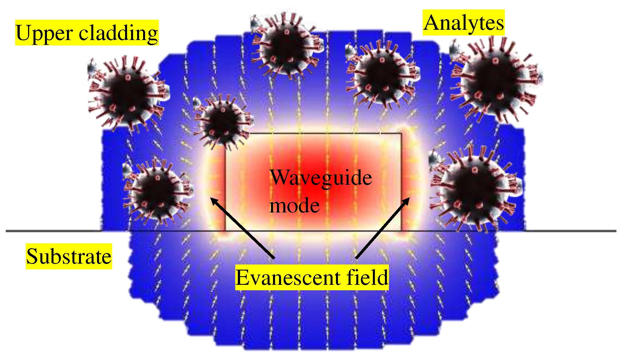
Figure 1. Illustration of the WG evanescent field interacting with the analytes in the ambient medium.
Preprints 98348 g001
Figure 2. Normalized E-field distribution in the WG geometry at an operational wavelength of 1550 nm, (a) ridge WG of dimensions W × H=450 × 250 nm, (b) slot WG of dimensions W × H=270 nm × 250 nm and a gap=50 nm, (c) modified ridge WG geometry of dimensions W × H=450 nm × 250 nm with a 25 nm buffer layer between gold layer and WG core.
Preprints 98348 g002
Figure 3. EFR calculation for (a) SOI ridge WG, (b) Si3N4 ridge WG, (c) SU-8 ridge WG.
Preprints 98348 g003
Figure 4. (a) Relationship between EFR/sensitivity and WG geometry, (b) EFR versus refractive index of material platform.
Preprints 98348 g004
Figure 5. The MIR absorption spectra of specific compounds are characterized by their relative intensities. In this context, H2O represents water, CO2 stands for carbon dioxide, CO denotes carbon monoxide, NO represents nitric oxide, NO2 signifies nitrogen dioxide, CH4 corresponds to methane, O3 indicates oxygen, and NH3 stands for ammonia[68].
Preprints 98348 g005
Figure 6. (a) Illustration of the structures of three distinct slot WGs employing Ge-on-CaF2 materials: (a) a conventional slot WG [77], (b) a partial-strip-loaded slot WG [77], and (c) a full-strip-loaded slot WG [77], (d-g) Normalized E-field distribution in dual hybrid plasmonic WG and at different segments of the WG[34], (h) Optical microscope image from the top view showcasing the fabricated WG [3], (i) Cross-sectional SEM image of the WG. The fabrication process has yielded a membrane with dimensions of 130 µm width and 350 nm thickness [3].
Preprints 98348 g006
Figure 7. (a) Depiction of the BiMW biosensor designed for the direct detection of the entire SARS-CoV-2 virus, employing bioengineered nanobodies (Nb) as recognition elements [98], (b) Schematic representation of the sensing principle underlying the BiMW interferometer [98], (c) Image of the BiMW sensor chip, with a 1 Euro coin included for dimension comparison [98], (d) Photo of the laboratory setup for conducting BiMW biosensing measurements [98].
Preprints 98348 g007
Disclaimer/Publisher’s Note: The statements, opinions and data contained in all publications are solely those of the individual author(s) and contributor(s) and not of MDPI and/or the editor(s). MDPI and/or the editor(s) disclaim responsibility for any injury to people or property resulting from any ideas, methods, instructions or products referred to in the content.
Copyright: This open access article is published under a Creative Commons CC BY 4.0 license, which permit the free download, distribution, and reuse, provided that the author and preprint are cited in any reuse.
Prerpints.org logo

Preprints.org is a free preprint server supported by MDPI in Basel, Switzerland.

Subscribe

© 2024 MDPI (Basel, Switzerland) unless otherwise stated