1. Introduction
AlGaN-based nitride semiconductors exhibit a direct band transition and offer a tunable broadband gap spanning from 3.4 eV to 6.0 eV, achieved by controlling the mole fraction (x) of Al. This wide range covers three distinct ultraviolet (UV) regions, namely UV-A (320–400 nm), UV-B (290–320 nm), and UV-C (200–290 nm) [
1,
2]. The versatile properties of AlGaN make it highly suitable for various optoelectronic applications, including ultraviolet light-emitting diodes (LEDs), laser diodes (LDs), and solar-blind avalanche photodiodes (APDs) [
3,
4,
5,
6]. Moreover, owing to its remarkable two-dimensional electron gas (2DEG) density and mobility, the AlGaN/GaN channel enables the realization of high-power electronic devices for applications in RF power and switching electronics [
7,
8,
9]. Consequently, comprehensive investigations into the growth and material characterization of AlGaN hold significant importance for the advancement of AlGaN-based devices.
In comparison to visible light-emitting diodes (LEDs), AlGaN-based LEDs still encounter challenges such as low quantum efficiency resulting from high dislocation density and poor hole injection efficiency [
10,
11,
12,
13]. The radiative efficiency, which quantifies the generation of UV photons through radiative recombination in relation to competing non-radiative processes, plays a crucial role [
14]. Non-radiative recombination centers, including threading dislocations and point defects arising from varied growth conditions or lattice mismatch, can hamper the quantum efficiency of AlGaN devices [
15,
16,
17,
18]. Consequently, the optimization of AlGaN-based LEDs necessitates a thorough understanding of material quality and optical characterization. Photoluminescence (PL) and time-resolved photoluminescence (TRPL) measurements serve as vital analytical techniques [
19,
20]. Numerous research groups have investigated PL spectroscopy of AlGaN alloys grown via metal-organic vapor phase epitaxy (MOVPE) [
21,
22,
23]. Molecular beam epitaxy (MBE), being a crucial epitaxial technique, offers unique advantages in fundamental research owing to its ultra-high vacuum conditions and employment of ultra-high purity metal sources [
24,
25,
26]. Epitaxial growth conditions, including growth temperature, growth mode, and V/III ratio, significantly impact material quality [
27]. While our previous work explored the growth kinetics and optical properties of MBE-grown AlGaN, a detailed understanding of the specific influence of growth temperature on the optical properties of AlGaN necessitates further investigation.
This study investigates the influence of growth temperature on the optical properties of AlGaN structures grown using plasma-assisted molecular beam epitaxy (MBE). The 325 nm AlGaN is characterized using high-resolution atomic force microscopy (AFM), X-ray diffraction (XRD), photoluminescence (PL), and time-resolved photoluminescence (TRPL). An AlGaN sample grown at a relatively elevated temperature with precise control of Al and Ga flux demonstrates enhanced surface quality, intensified PL emission, and prolonged minority carrier lifetime. The optical properties of the AlGaN materials emitting at 325 nm are comprehensively examined, revealing the presence of two distinct non-radiative recombination centers characterized by different activation energies. The minority carrier lifetimes of the AlGaN material are measured to be 560 ps at 10 K and 64 ps at room temperature, exhibiting an S-shaped temperature-dependent trend. The underlying mechanism is analyzed from the perspective of carrier dynamics.
3. Results and Discussion
The fabrication of high-quality AlGaN materials poses greater challenges compared to the epitaxial growth of GaN. This difficulty stems from the relatively large surface adhesion coefficient of Al atoms, which leads to their low migration rate on the growth surface and their tendency to remain near the initial positions. Consequently, three-dimensional island growth occurs, resulting in the formation of high-density defects such as grain boundaries and dislocations. To overcome these challenges, higher growth temperatures are typically required for AlGaN compared to GaN. The impact of temperature on AlGaN materials has been investigated across different temperature ranges. In this study, Samples A was grown in the lower temperature range, with growth temperature of 725°C. Samples B and C were grown in the higher temperature range, with growth temperatures of 750°C and 765°C, respectively.
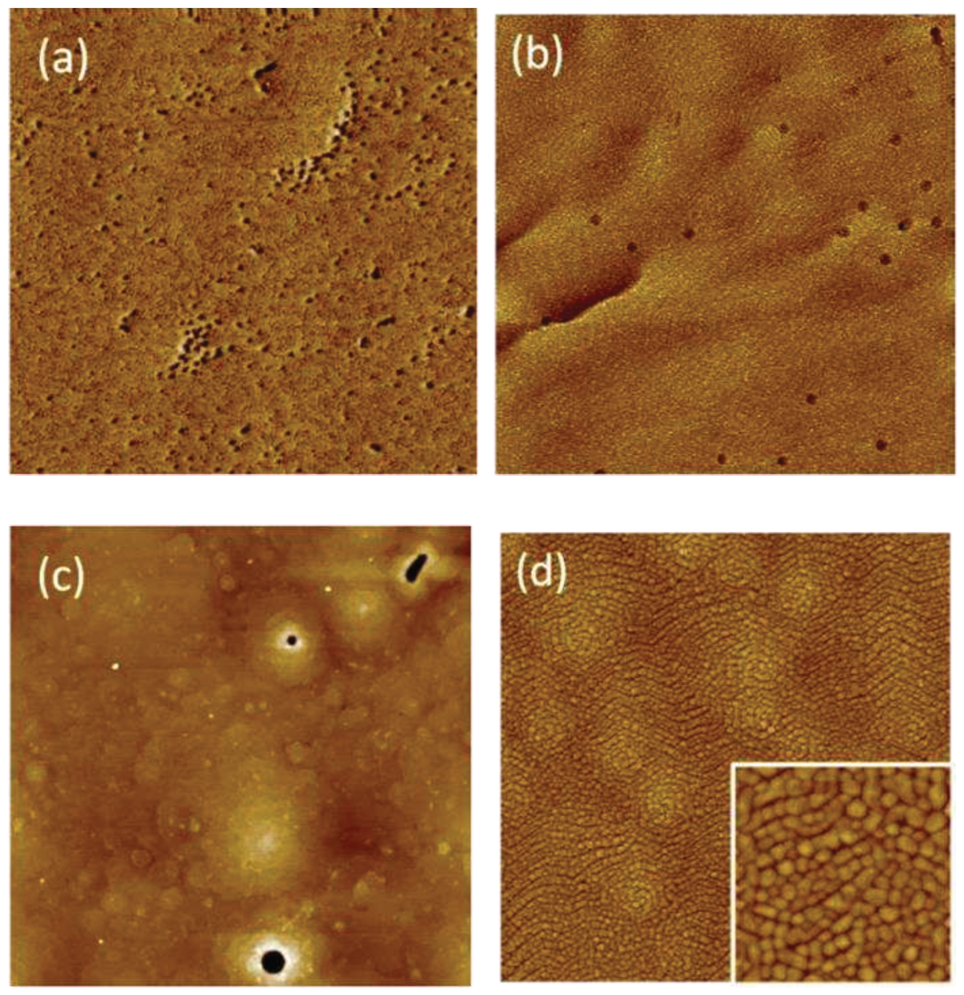
Figure 1 presents the atomic force microscopy (AFM) images of the four samples, revealing the root mean square (RMS) values for surface roughness as 1.68 nm, 0.74 nm, 0.94 nm, and 1.47 nm, respectively.
From
Figure 1a,b, it can be observed that both Samples A and B exhibit surface pits, with Sample A having an order of magnitude higher pit density than Sample B. This disparity arises due to the enhanced migration of Al atoms on the surface at higher substrate temperatures, allowing for diffusion to low-energy sites such as steps and kinks, promoting two-dimensional layer-by-layer growth. This growth mode effectively suppresses the formation of crystal facets and dislocations, thereby reducing surface pits and achieving a smoother surface morphology.
However, contrary to Sample C, the surface of sample D, which was grown at a higher temperature, becomes rougher. Microscopic analysis, combined with the images of the two samples, was performed. At a magnification of 50 times, it can be observed that metallic droplets are formed on the surface of Sample C, while the heated Sample D does not exhibit such droplets. Therefore, it can be inferred that Sample C was grown under metal-rich conditions. During the actual growth process, excess Ga atoms form a coverage layer of 0-3 monolayers in thickness at the growth front, serving as an active layer that facilitates long-range migration and diffusion of Al atoms on the surface [
28].
Figure 1c demonstrates that the surface of Sample C is exceptionally smooth, lacking the grain-like morphology observed in other samples. However, as the temperature is increased to 765°C, a significant amount of Ga on the surface begins to desorb and evaporate, making it impossible to maintain the metal coverage layer. This can even lead to N-rich conditions, resulting in a visibly roughened material surface and the formation of crystal facets and screw-type dislocations. The inset in
Figure 1d presents an AFM scan of Sample D within a 1.5 μm × 1.5 μm area, revealing incomplete merging of grains and a high density of grain boundaries, which contributes to the roughening of the surface. These findings suggest that the chosen growth temperature should facilitate the migration and diffusion of Al atoms on the growth surface while avoiding excessively high temperatures that could lead to Ga desorption or even result in N-rich conditions.
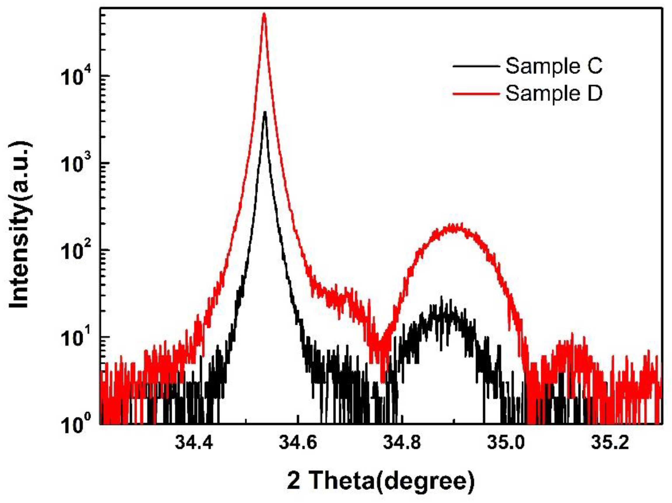
Figure 2 shows the HRXRD (002) plane scan results of Sample C and Sample D. The composition of Sample B, Sample C and Sample D are 26.5%. The diffraction peak positions of the two samples are identical, indicating that the increase in growth temperature does not affect the Al composition of the AlGaN material. Additionally, the XRD diffraction spectrum exhibits distinct satellite peaks, indicating the presence of relatively steep heterointerfaces between the AlGaN epitaxial layer and the GaN layer.
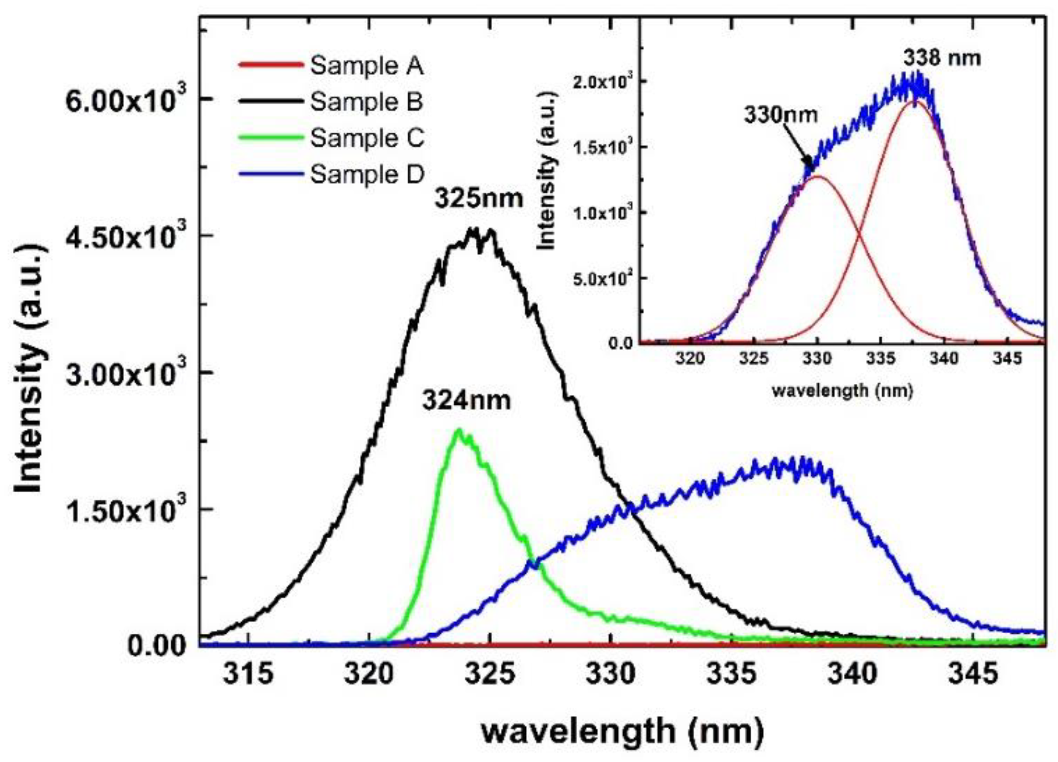
The low-temperature PL spectra of the four samples are shown in
Figure 3. Sample B exhibits a peak wavelength at 325 nm (corresponding to an energy of 3.82 eV) with a full width at half maximum (FWHM) of 9.5 nm (113 meV). However, Sample A does not exhibit a corresponding emission peak, further confirming the presence of a significant number of defects acting as non-radiative recombination centers in Sample A material. From the XRD test results, it is determined that Samples C and D have the same Al composition; therefore, these two samples should exhibit intrinsic emission peaks at the same wavelength. However,
Figure 3 reveals that Sample C exhibits a emission wavelength of 324 nm, which corresponds to the intrinsic emission peak. In the inset, it can be observed that Sample D exhibits two emission peaks at wavelengths of 330 nm and 338 nm, respectively. This suggests that the two emission peaks in Sample D are caused by donor-acceptor transitions at different energy levels. These energy levels can be caused by the non-uniformity of alloy components due to excessively high growth temperatures, or by impurities, defects, etc.
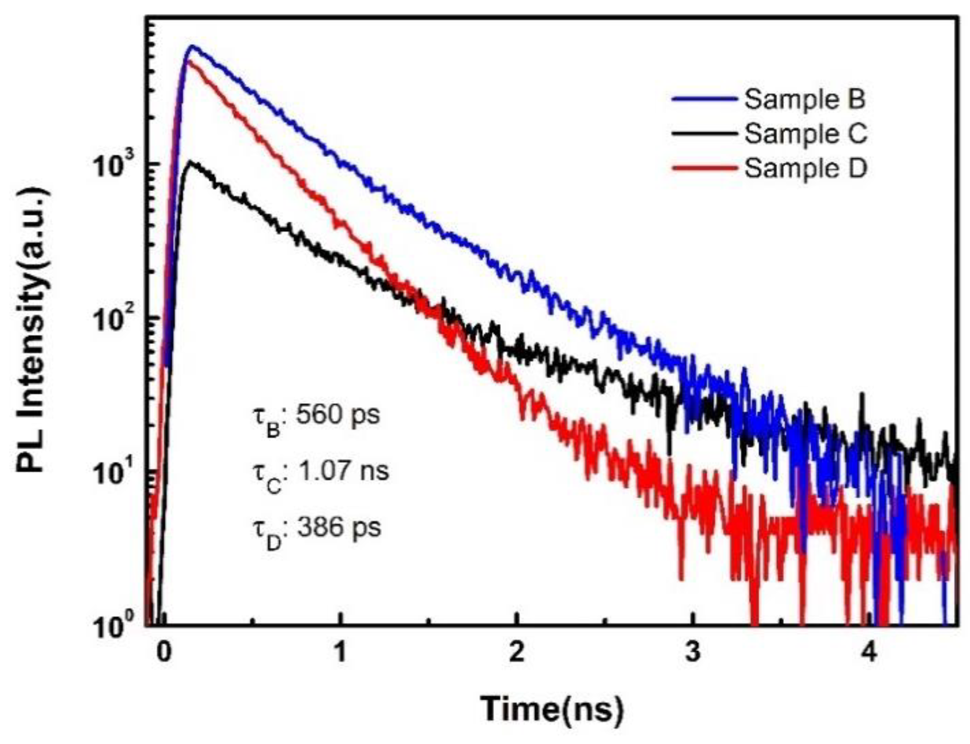
Figure 4 shows the time-resolved PL spectrum of samples B, C and D at 10 K. By analyzing the intensity variation in the time-resolved PL spectra, the minority carrier recombination lifetime can be calculated. The formula for calculating the carrier lifetime is as follows:
I represents the PL intensity, τ is the recombination lifetime of the carrier. The carrier relaxation time of sample B is 560 ps according to TRPL fitting. Wile, the relaxation time of sample C and D is only 1.07 ns and 386 ps, respectively. The short lifetime of the minority carriers is not conducive to fabricating devices with high luminous efficiency. The PL lifetimes of Sample C were evaluated using the fit obtained from the double-exponential function. The fitting results show that the two coefficients of τ1 and τ2 are 375 ps and 1.07 ns, respectively. The faster decay coefficient represents the radiative recombination of free excitons or localized excitons bound to shallow traps, while the slower coefficient corresponds to nonradiative recombination processes involving defects or impurities.
From the above analysis, it can be seen that Sample B has good crystal quality and surface morphology. The ultrafast optical properties of AlGaN material (Sample B) in the range of 10 to 300 K were studied using variable temperature PL and TRPL spectra.
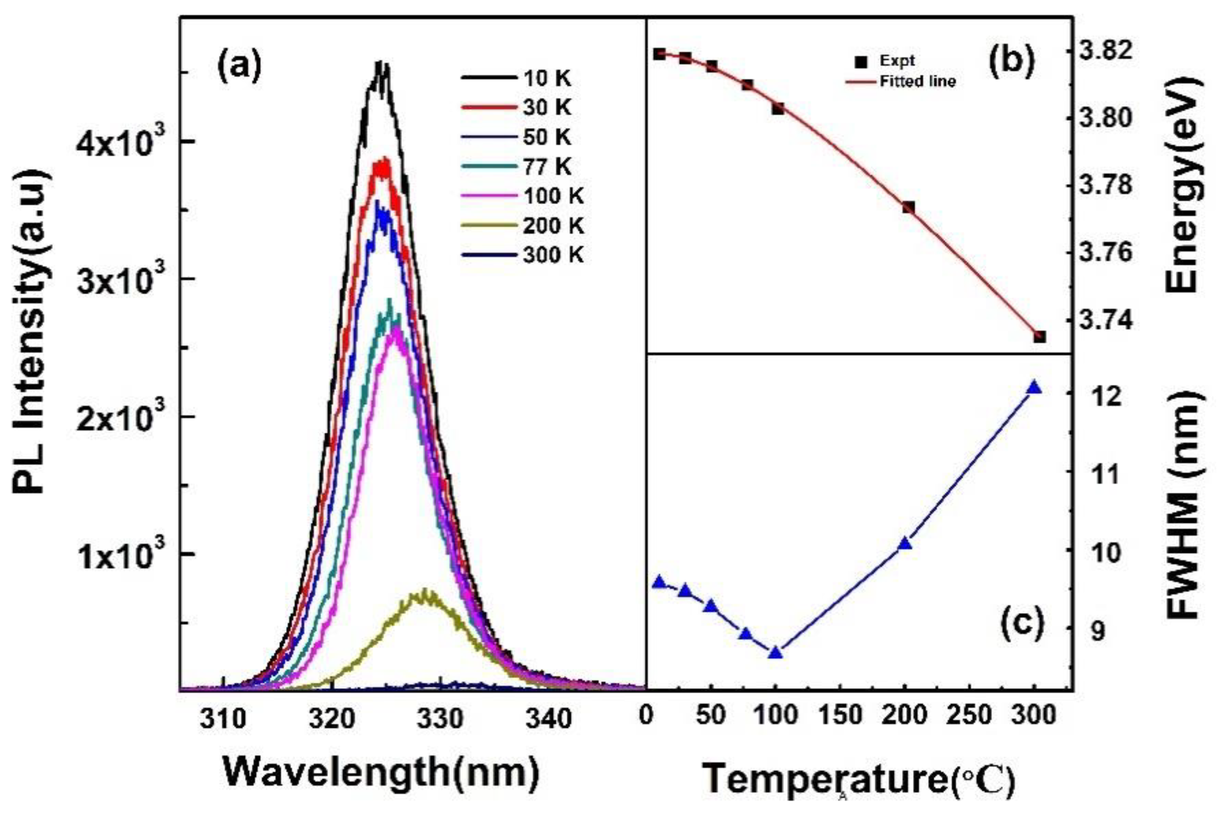
Figure 5a shows the PL spectra of AlGaN samples at different temperatures. With increasing temperature, the PL peak of the AlGaN sample undergoes a red shift. The wavelength of the luminous peak is 332 nm at room temperature, corresponding to an energy of 3.74 eV. The relationship between peak position energy and temperature is shown in
Figure 5b, which corresponds to Varshni’s [
29] empirical formula. The expression is:
where Eg(T) and Eg(0) are band gaps at a temperature T(K) and T = 0 K. α and β are Varshni thermal coefficients. By data fitting we can get a value of 0.30 meV/K and 206 K, which is close to the reported value [
30].
Based on the variable temperature photoluminescence (PL) spectra, the full width at half maximum (FWHM) of each temperature-dependent emission wavelength was obtained through Gaussian fitting, as shown in
Figure 5c. The broadening of the emission peak exhibits a decreasing trend initially with increasing temperature, followed by a rapid increase. The variation of PL spectrum broadening with temperature is primarily associated with the transfer and distribution of carriers among localized states in the AlGaN crystal material. Numerous localized state centers caused by lattice defects and compositional non-uniformities exist within the AlGaN crystal material, each possessing different energy level depths. In semiconductor materials, at low temperatures (10 K), carriers are frozen onto different localized centers. Therefore, during the photoluminescence measurement, the energy level differences of these localized state centers result in the broadening of the PL spectrum. As the temperature increases to 100 K, the kinetic energy of the carriers increases, allowing carriers in shallow energy valleys to break free from their localized centers and transfer to deep energy valleys with lower energy levels. This leads to a more concentrated carrier distribution, thereby reducing the broadening of the PL spectrum caused by the energy level differences of the localized state centers. However, as the temperature continues to rise, the carrier’s kinetic energy becomes larger, causing carriers in the deep energy valleys to overcome the binding barrier and distribute into other energy valleys, resulting in a more dispersed carrier distribution. During the radiative recombination process, carriers can relax to the deep energy valleys and undergo radiative recombination or directly undergo radiative recombination in the shallow energy valleys. This leads to an increased broadening of the PL spectrum.
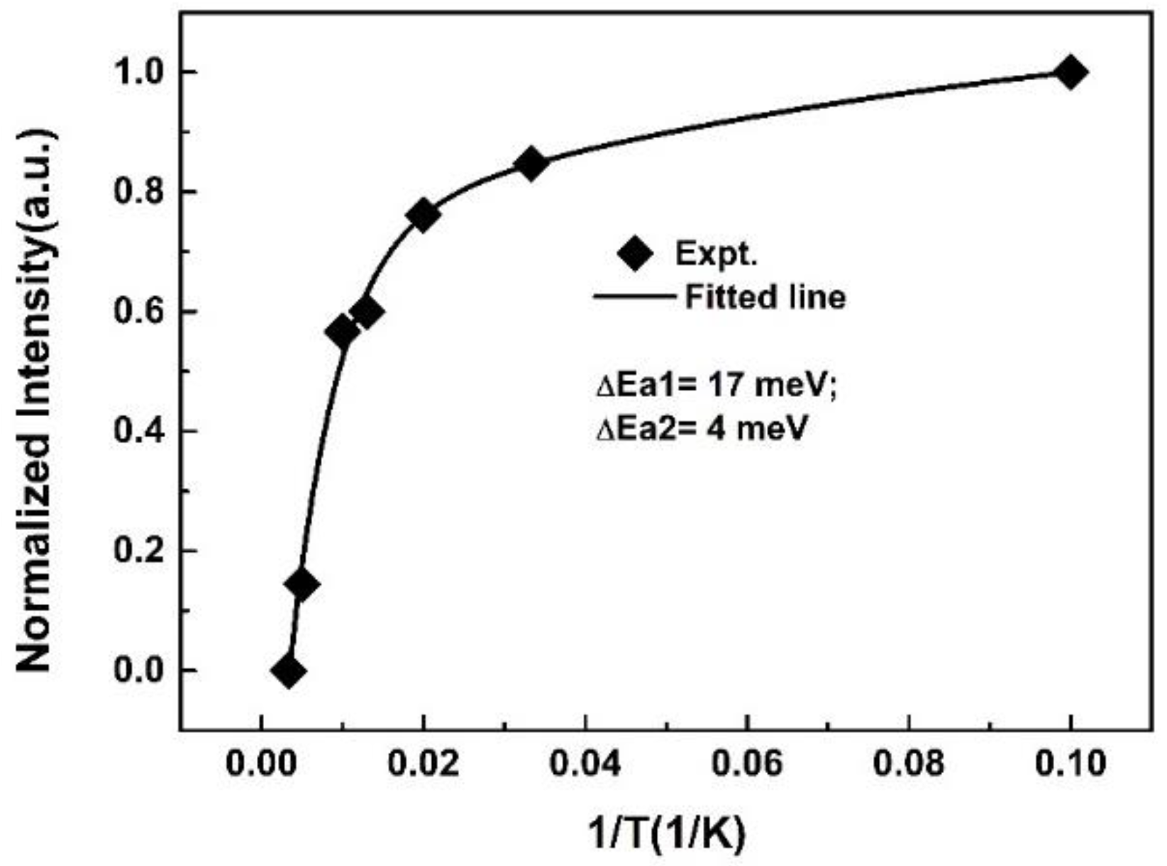
In addition to the peak shift, the PL spectrum exhibits a decrease in emission intensity with increasing temperature, primarily due to the temperature quenching effect caused by the enhanced nonradiative recombination. For variable temperature PL spectra involving nonradiative recombination processes, the variation of emission intensity with temperature follows the Arrhenius equation [
31]:
where
I(T) is the temperature-dependent integrated PL intensity, I
0 is the integrated PL intensity at low temperatures, K
B is the Boltzmann’s constant, and C is a rate constant.
Figure 6 illustrates the fitting of formula (3) to the experimental data, revealing the necessity of incorporating two radiative recombination centers for improved model accuracy. The non-radiative recombination centers exhibit activation energies of 17 meV and 4 meV, accompanied by corresponding C values of -1.22 and -0.43, respectively. A lower activation energy indicates a higher likelihood for carriers to escape from the localized state center and transition to the non-radiative recombination center, consequently diminishing the internal quantum efficiency of the optical materials. The integral intensity of PL luminescence decreases with increasing temperature and decreases faster at high temperature. The integral intensity at room temperature is only 1.1% of that at 10 K, which is consistent with the range reported in the literature [
2]. Further optimization of the conditions is required to reduce the defect density and obtain AlGaN thin film materials with better optical properties.
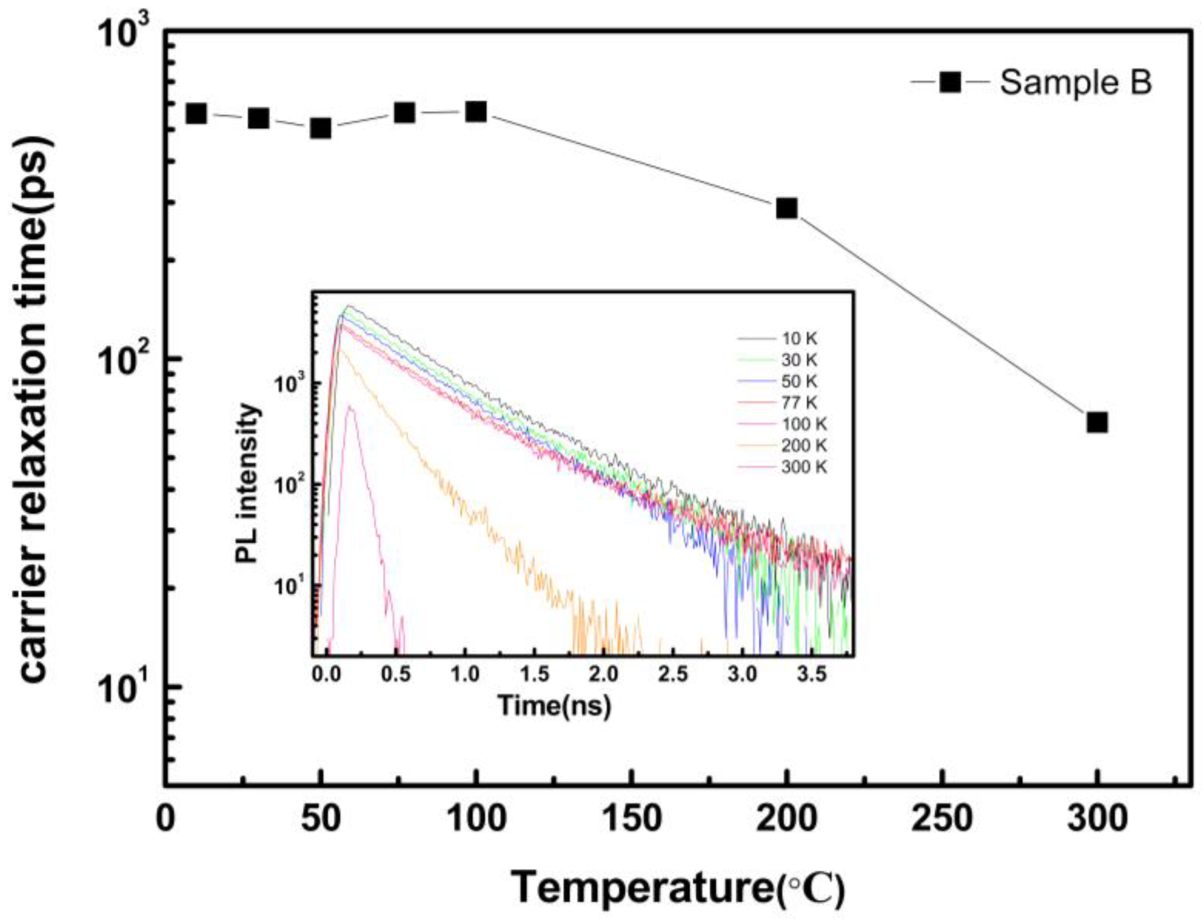
Figure 7 illustrates the temperature-dependent relationship between the minority carrier lifetime of the AlGaN sample. The inset presents the TRPL spectra measured at various temperatures. In the low-temperature range (10 K to 50 K), the TRPL spectra exhibit characteristics of a double exponential decay, indicating the presence of two recombination mechanisms associated with two relaxation times: a shorter relaxation time, denoted as τ
1, and a longer relaxation time, denoted as τ
2. The shorter relaxation time τ
1 corresponds to a rapid relaxation process, likely attributed to localized bound excitonic recombination that prevails only at low temperatures and diminishes above 50 K. The longer relaxation time τ
2 exhibits a non-monotonic, S-shaped temperature dependence. Below 50 K, the minority carrier lifetime declines with increasing temperature during the low-temperature stage. Subsequently, as the temperature rises beyond 50 K to 100 K, the minority carrier lifetime exhibits an increasing trend. However, beyond 100 K, the minority carrier lifetime experiences a rapid decline with temperature, reaching a mere 64 ps at room temperature.
The mechanism of this phenomenon can be analyzed from the perspective of carrier dynamics. According to the carrier recombination theory, when non-equilibrium carriers are injected into the semiconductor, its relaxation time τ is:
At low injection, the non-equilibrium carrier concentration is far less than the intrinsic carrier content Δp << (n
0 + p
0). For general recombination centers, r
n and r
p show little difference, Δ P can be ignored. The assumptions allow a simplification of equation (4).
Unintentionally doped AlGaN is n-type, which n
0, n
1 >> p
0, p
1, and the relation between n
0 and n
1 is
The above equation is further simplified as
For non-degenerate n-type semiconductor materials, the Fermi level is
Relaxation time is generally written like this for convenience:
where a and b are positive numbers.
Based on the temperature-dependent relationship between the integrated intensity of the PL spectrum and temperature, two distinct non-radiative recombination centers can be identified in AlGaN semiconductor materials. These centers exhibit activation energies of 4 meV and 17 meV, respectively, classified as class I and class II. The activation energy of the class I non-radiative recombination center is exceptionally low, enabling gradual activation even at low temperatures. As the concentration of non-radiative recombination centers increases, the lifetime of minority carriers diminishes. At 50 K, the type I non-radiative recombination center becomes fully ionized, while the type II non-radiative recombination center with a higher activation energy remains inactive. According to formula (9), the minority carrier lifetime increases with temperature. As the temperature exceeds 100 K, the type II non-radiative recombination center begins to ionize and assumes a dominant role. The deeper the position of the recombination center, the greater its impact on the minority carrier lifetime, resulting in a rapid decrease. Therefore, for enhanced luminous efficiency of AlGaN materials, it is crucial to eliminate non-radiative recombination centers at 14.5 meV and other deep-level defects.
Author Contributions
Conceptualization, W.Y.; Methodology, W.Y., P.D., J.Z., and S.L.; Validation, P.D. and W.Y; Formal analysis, P.D. and W.Y.; Investigation, W.Y., P.D., J.Z., and S.L.; Resources, W.Y. and S.L.; Data curation, W.Y. and P.D.; Writing–original draft, W.Y., and P.D.; Writing–review and editing, W.Y., P.D., J.Z., and S.L.; Visualization, W.Y., and P.D.; Supervision, W.Y., P.D. and S.L.; Project administration, W.Y., P.D. and S.L.; Funding acquisition, W.Y., P.D. and S.L. All authors have read and agreed to the published version of the manuscript.
