1. Introduction
A wireless sensor network (WSN) is a
wireless network with a large number of infrastructure-less wireless sensors
deployed in an ad hoc manner, where each sensor node is used to monitor system,
physical, or environmental conditions in a specific area [
1]. The nodes in any WSN contain sensor interfaces,
computing devices, transceivers, and power devices. These devices perform
important tasks by enabling the nodes to communicate with each other and
transmit data obtained from sensors. The need for this system leads to the
development of the concept of the Internet of Things (IoT). The concept of IoT
makes it possible to have instant access to environmental data, which greatly
improves efficiency and productivity in many processes [
2].
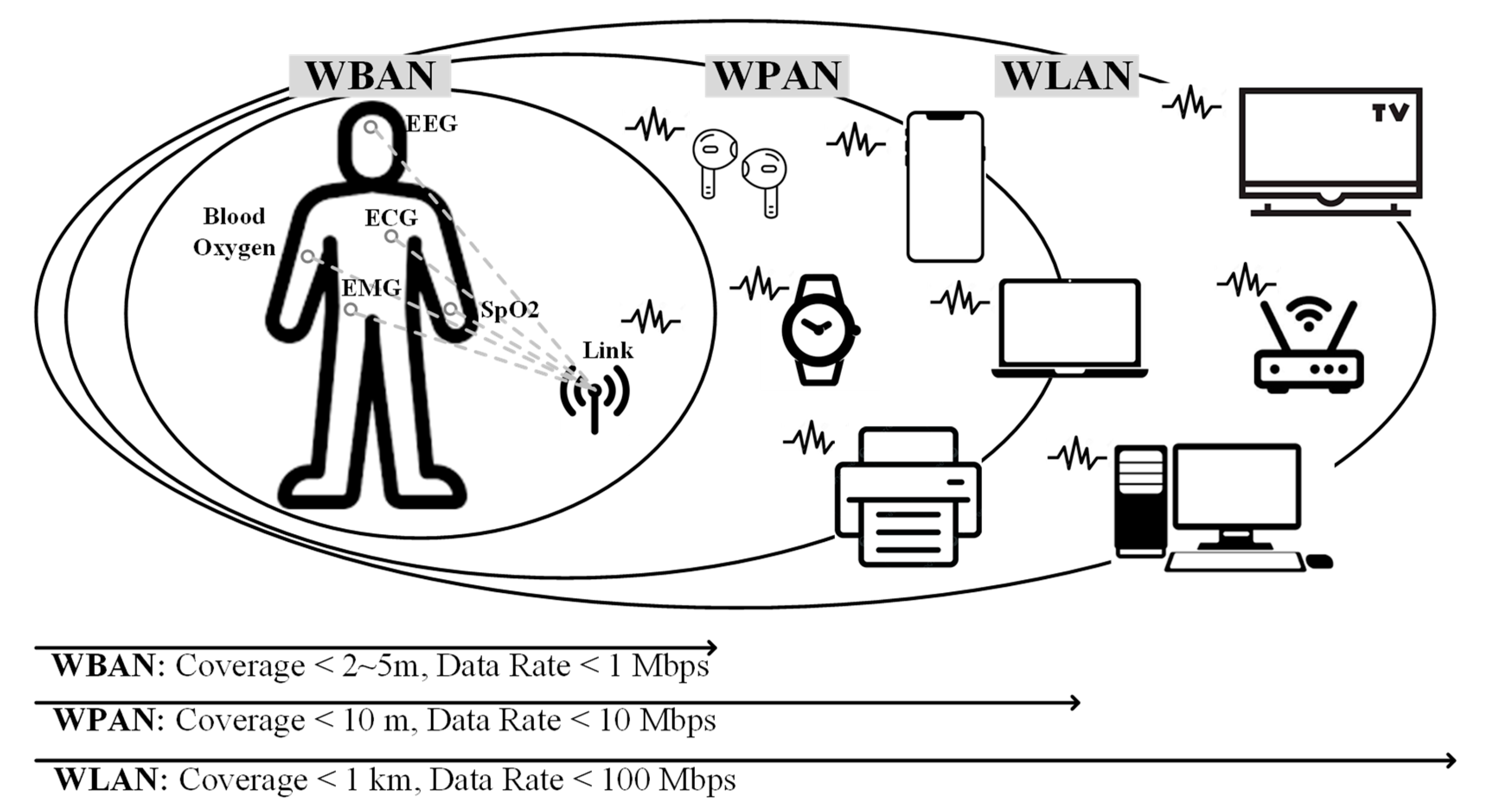
The sensor nodes support both wireless
personal area networks (WPANs) for long-range applications, such as smart homes
[
3], and wireless body area networks (WBANs)
for short-range applications, such as low-data medical monitoring [
4] as shown in
Figure 1. Bluetooth Low Energy (BLE) or Zigbee using long-range
energy-efficient wireless systems [
5,
6,
7,
8] are
the most widely used for WPANs. Most wireless transmitters (TXs) are optimized
to be the most efficient at the output power of 10 dBm or more for WPAN applications
to achieve high efficiency, so they are less efficient at the lower output
power of around -20 dBm required for WBAN applications. As IoT sensor nodes
become more ubiquitous, the sensor node systems need to support both WPANs and
WBANs with high efficiency to maximize battery life.
The most vital and energy-hungry part is
the power amplifier (PA) which consumes more than 50% of the available power in
the IoT sensor node [
9]. This serves as the
major cause of low battery life in any wireless transceiver. Switched-mode
power amplifier architectures are commonly used for IoT applications since the
phase-modulated signals used in such systems do not have any amplitude
information. Popular architectures are class-D [
10,
11,
12,
13]
and class-E/F power amplifiers (PAs) [
14,
15].
Class-E/F PAs usually use cascading for reliability concerns and more
complicated off-chip matching networks for harmonic suppression [
16]. Class-D PAs are more suitable for applications
targeting output powers around 10 dBm with robust matching and no reliability
concerns. Therefore, the output power control across a wide range of > 30 dB
remains a challenge.
PAs also generate electromagnetic waves at
unintended frequencies. Strong harmonic spurious emissions can potentially
contaminate the out-of-band spectrum, causing receivers (RXs) operating at the
same harmonic frequencies to desensitize. For
example, the second harmonic (HD2) of a 2.4 GHz TX is located at the N79 band
of a 5G NR [
14].
As a sensor node operating in the industrial, scientific, and medical (ISM)
band, Spurious emissions are categorized as any electromagnetic emissions that
occur at frequencies that are not intentionally emitted, especially for
electronics that intentionally emit one or more frequencies. Therefore, all
electronics are required to be tested to ensure that they do not emit
electromagnetic waves of excessive intensity at all frequencies except those at
which they are intentionally emitted, which is known as electromagnetic
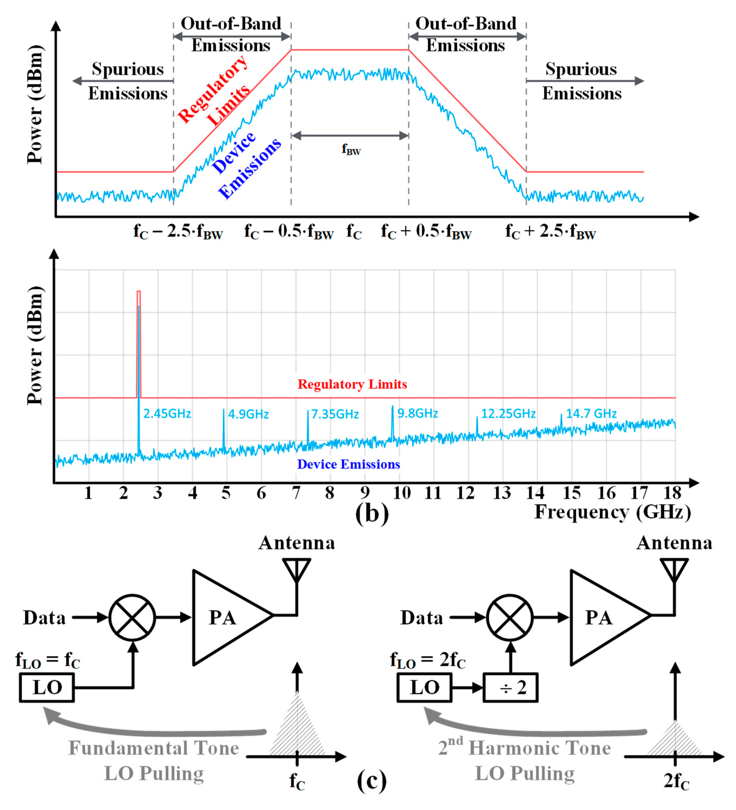
compatibility (EMC) testing. Furthermore, the TX must meet more stringent
harmonic levels corresponding to conducted power of < -41.2 dBm as shown in
Figure 2(b). When a
PA is integrated on the same chip with a voltage-controlled oscillator (VCO),
as shown in
Figure 2(c) if the PA output frequency and local oscillator (LO)
frequency are the same, the high output of the fundamental frequency of the PA
causes pulling for the LO. Even when the operating frequency of the PA is half,
the second harmonic of the PA can cause the VCO pulling [
17].
This paper introduces a TX with a digitally
controllable current-mode Class-D (CMCD) power amplifier (PA), second-harmonic
distortion (HD2) super-compression, and passive filters for harmonic component
reduction. It addresses a wide range of output powers for various IoT
applications and the second harmonic distortion affecting other bands and VCO
pulling in the ISM band at 2.4 GHz. This article is organized in the following
manner.
Section 2 presents an overview of
class-D power amplifiers.
Section 3
describes the overall block diagram of the proposed TX and the wideband CMCD PA
with harmonic suppression technique.
Section 4
discusses the experimental results of the proposed TX obtained on the
integrated circuit fabricated in 28 nm CMOS technology. Finally, the main
contributions are summarized in
Section 5.
2. Class-D Power Amplifier Overview
Switched-mode PAs have the characteristic
that the product of the voltage and current waveforms applied to the transistor
becomes zero, so the power consumed by the transistor becomes zero, showing a
theoretical efficiency of 100%. However, the theoretical high efficiency cannot
be obtained due to the effect of parasitic components present in the
transistor, and the loss due to parasitic components increases as the operating
frequency increases, which limits its use in high-frequency bands. Class-E/F
power amplifiers have received a lot of attention as amplifiers for wireless
power transmission systems due to their ease of use, heat dissipation, and
simple structure, but it is difficult to realize high output power compared to
other power amplifiers and requires switch elements with high breakdown voltage
due to high drain-source peak voltage [
18].
Unlike Class-E/F power amplifiers, Class-D has the characteristic that the
output current decreases as the load impedance increases, so the losses in the
transistors are relatively small, so the change in efficiency with the change
in load impedance is small.
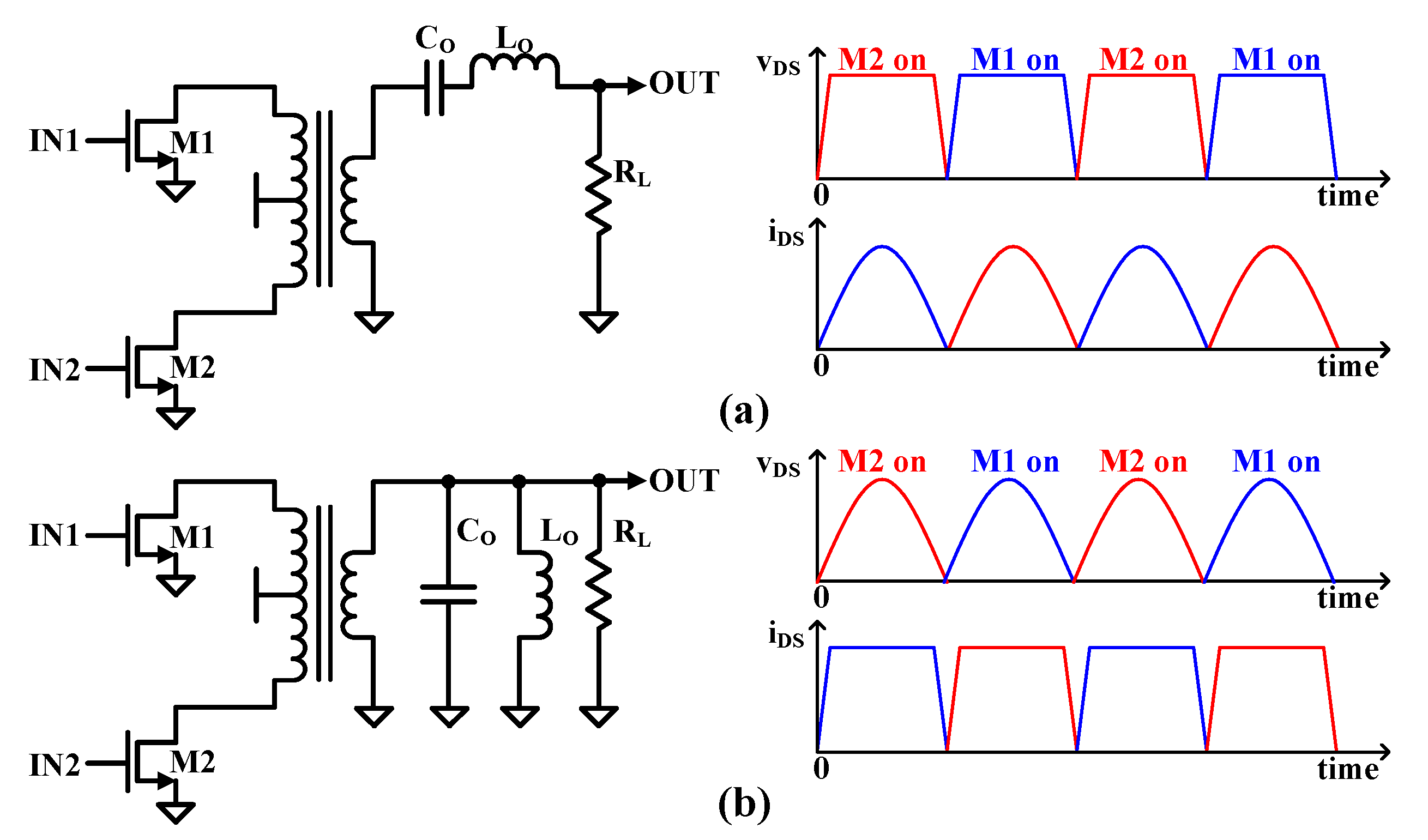
The class-D power amplifiers are
categorized as voltage-controlled and current-controlled. As shown in
Figure 3(a), a voltage-mode class-D (VMCD) PA
operates two transistors by switching each transistor on and off with a 180˚
phase difference, which causes the drain voltage waveform to be a square wave,
and only the desired frequency components are delivered to the load through a
series resonant circuit connected to the load. The series filter has a resonant
frequency that is set to the center frequency of the output signal. The voltage
across the transistor is a square wave and the transistor current will be a
half-wave rectified sine wave, which is theoretically 100% efficient. However,
the efficiency of the transistor can be reduced if there is some parasitic
drain-source capacitance (C
DS) present in the transistor that must
be charged, discharged, or grounded through the transistor. This means that the
voltage waveform will not have a perfectly square shape, and some transient
current spikes will occur when the transistor turns on. The overlap of voltage
and current is unavoidable. Energy dissipation is defined as 1/2C
DSV
DD2f
during each transistor closure cycle. This is why the class-D is not a popular
gigahertz amplifier. For the current-mode class-D (CMCD) PA as shown in
Figure 3(b), the two switching transistors
control the current instead of the voltage. Moreover, a parallel filter is set
to the center frequency of the output signal. The filter resonance causes
zero-voltage switching, and there is no voltage across the transistor during each
transistor closure cycle. There are filters connected in parallel and their
resonance frequency is set to the carrier frequency—the filter resonance results
in zero voltage switching with no voltage across the transistor at each
switching time. Even if the transistor has some output C
DS, the C
DS
can be part of the output parallel filter. Thus, current-mode Class-D power
amplifiers have high-efficiency characteristics and very small parasitic losses
for design PAs in the gigahertz range [
19].
3. Wide-Range CMCD PA with Harmonic Suppression
3.1. Transmitter Architecture
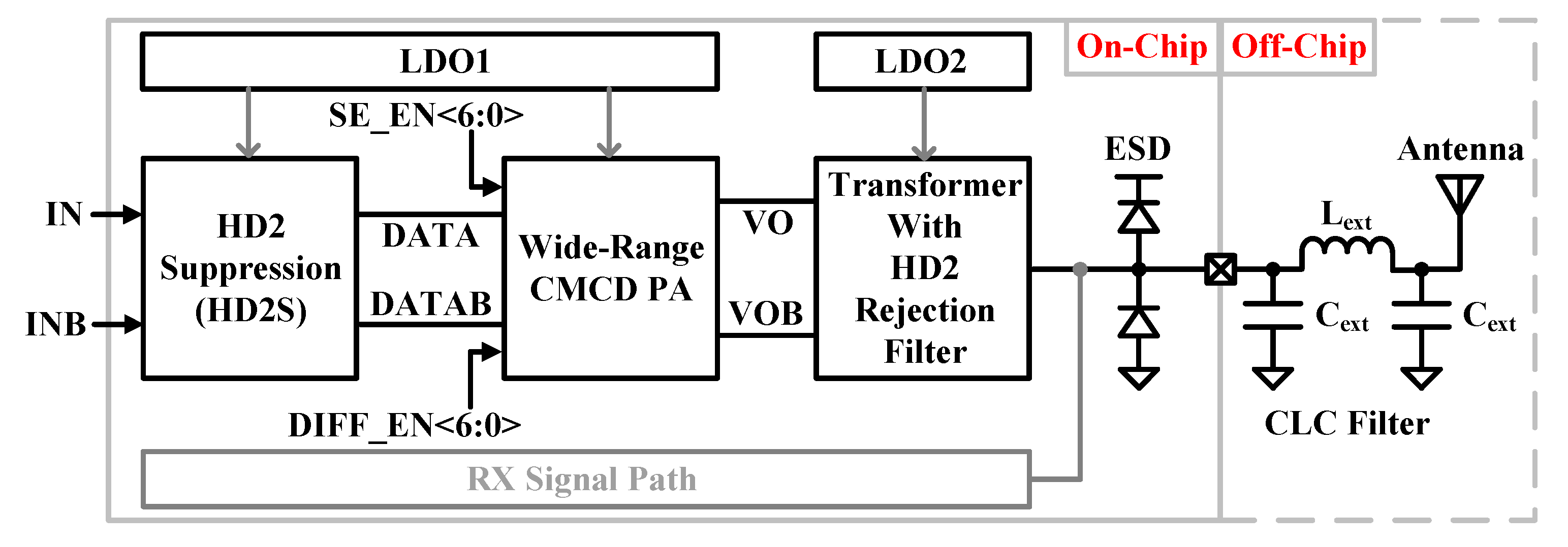
Figure 4
shows the proposed TX architecture. Gaussian minimum shift keying (GMSK) based
on two-point modulated data of a phase-locked loop is used for the differential
inputs (IN/INB) of the TX. The second harmonic suppression (HD2S) block is used
to reduce HD2, which can mitigate VCO pulling and meet out-of-band spurious
emissions, including second and third harmonic distortion (HD3) magnitudes
below absolute -41 dBm. The following CMCD PA
provides a wide range of output power with digital control signals of
SE_EN<6:0> and DIFF_EN<6:0>. The CMCD PA is connected to a
3:2 transformer (XFMR) to provide impedance matching and a differential signal
as a single-ended signal for driving an external antenna. The XFMR also
includes an LC parallel HD2 rejection filter to further reject HD2. Two low
dropout voltage regulators are used to provide stable supply voltages. The
first LDO output is assigned for thin oxide transistors that are used in all TX
blocks except the CMCD PA block. The second LDO output is connected to the XFMR
center tap to provide the power to the CMCD PA arrays using nMOSFET transistors
and isolate other circuitries from high-power PA. Two low-dropout voltage
regulators are used to provide a stable supply voltage, and their outputs are
1.0 V. A typical electrostatic discharge (ESD)
protection circuit with double diodes is added at the PAD. An external CLC π-type low-pass filter is added right next
to the external PAD to reduce harmonics additionally.
3.2. Wide-Range CMCD Power Amplifier
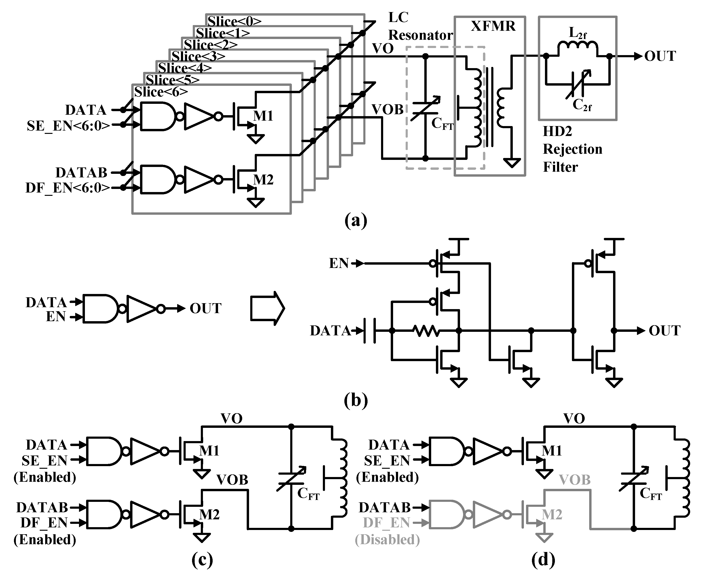
Figure 5(a)
shows a wide-range CMCD PA. The PA consists of two nMOSFETs to withstand the
high output. The C
DS of M1 and M2 can be designed to be included in
the capacitor of the LC resonator, which is a differential amplification load
for the tuned amplifier. The primary inductor (L
FTP) of the
transformer (XFRM) serves as the inductance in the CMCD PA tuning load also. As
shown in
Figure 5(b), an AND gate
consisting of a NAND and an inverter drives the nMOSFETs in the CMCD PA and
provides digital gain selection with the SE_EN<6:0> and DF_EN<6:0>
signals. The resistive feedback increases the 3 dB bandwidth compared to a
conventional static NAND gate. AC coupling completely blocks the common-mode level
of the clock signal to prevent propagation of duty cycle distortion.
Self-biasing of the crossover voltage restores the duty cycle to its ideal
value regardless of the input duty cycle. AC coupling combined with the
low-pass characteristics of the inverter produces bandpass characteristics. The
bandpass filter suppresses phase noise in the input data because it attenuates
all out-of-band noise. The digital variable gain PA is organized into 7-bit
binary slices to implement 127 differential output powers as shown in
Figure 5(c). The PA also supports a
single-ended mode to further fine-tune the gain steps as shown in
Figure 5(d). The DF signal coming into the
input is disabled to operate in single-ended mode within each slice, which
forces one side of the path (the negative side) to be turned off, resulting in
6 dB lower output power compared to differential mode.
3.3. Transformer and HD2 Rejection Filter
Figure 6(a)
shows the transformer (XFMR) and HD2 rejection filter inductor block used for
the proposed CMCD PA.
Figure 6(a) shows
the transformer (XFMR) and HD2 rejection filter inductor block used in the
proposed CMCD PA. The XFMR implements the main inductor and connection
crossings with two top metal lines while meeting the electrical migration
rules. A ring structure is added around the XFRM to reduce unwanted second
harmonic coupling to the nearby circuits including the HD2 rejection filter
inductor and the VCO inductor. A 3D electromagnetic simulation is performed to
obtain the extracted values of the XFMR and inductor, and the corresponding
schematics and their values are shown in Figure
6(b). The larger the inductance, the more favorable it is for increasing
the Q-factor of the resonant circuits. The switched capacitor (C
FT)
allows discrete frequency tuning for coverage of 2.4 GHz ISM band (2.4 ~ 2.48
GHz) resonating with parallel L
FTP. A 3:2 XFMR, n = 1.5, provides
impedance matching between the high output impedance of the PA and 50 Ω antenna
impedance in the TX mode.
The HD2 rejection filter is implemented as
an LC two-band stop filter or notch filter as shown in
Figure 5(a). The parallel LC components of L
2f
and C
2f exhibit high impedance at their resonant frequency, twice
the 2.4 GHz ISM band, so they block the HD2 signal from the load at that
frequency. Conversely, at other frequencies, they pass the signal to the load.
The resonant frequency of the HD2 rejection filter is expressed by equation
(1).
The
embedded low-loss switch scheme [
14] is applied for the use of a
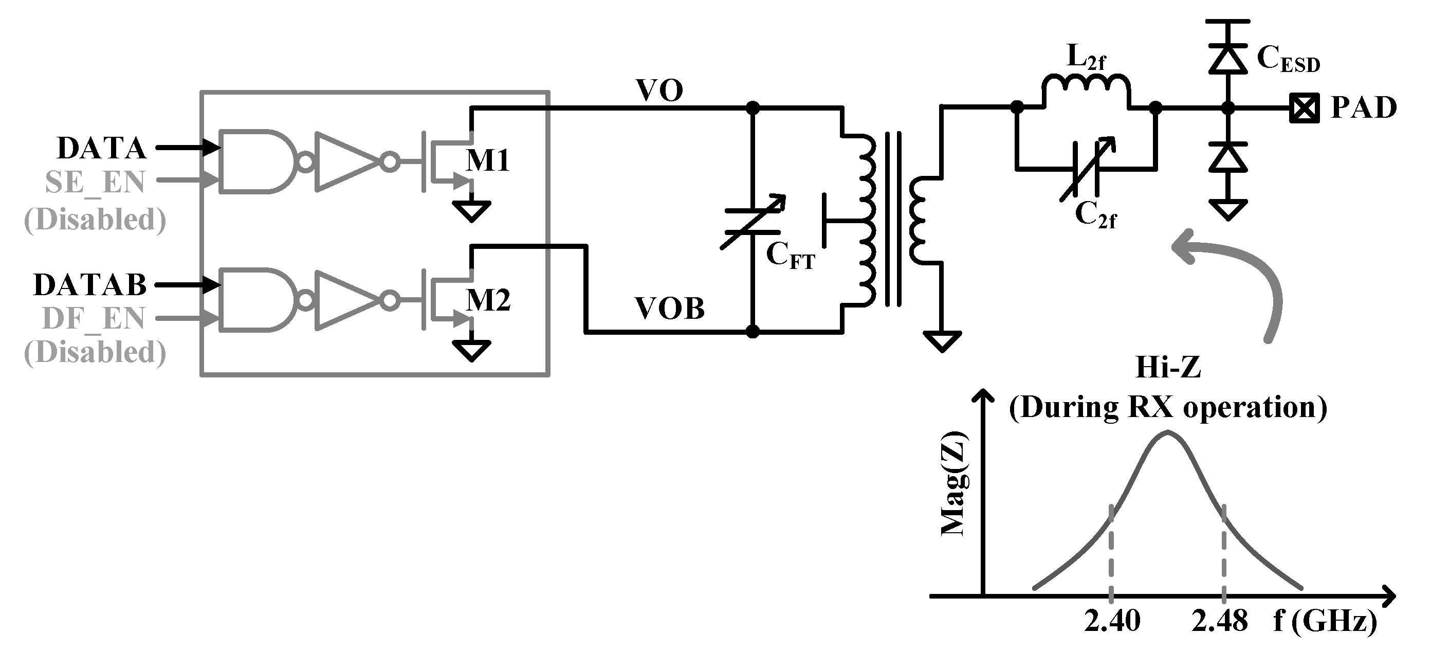
single antenna to support time division duplex (TDD) operation. The switch of
the proposed TX (TX_SW) has a high impedance of more than 300 Ωs within the 2.4 GHz ISM band in
RX operation mode as shown in
Figure 7. The XFMR multiplies the C
FT by the square of the primary to
secondary-turn ratio (n
2). All PA slices are disabled,
and the n
2
C
FT output
capacitance by the XFMR plus the 50% ESD capacitance (C
ESD) at the
PAD due to the RX sharing model resonates with the secondary inductance (L
FTS) of the XFMR to ensure that the
TX has a high output impedance during RX operation. The CFT must support
different capacitance values during TX and RX operations. A typical capacitance
is about 1200 fF in TX operation mode and about 450 fF in RX operation mode.
Therefore, the C
FT must accommodate a wide
capacitance tuning range, which limits the increase in inductance value to
increase the Q-factor of the XFMR, so half of the L
FTP in the
proposed TX is set to about 1.5 nH. The resonance frequency of the TX_SW is
given by equation (2), and the frequency is tuned at around 2.44 GHz to get
high impedance during RX operation mode.
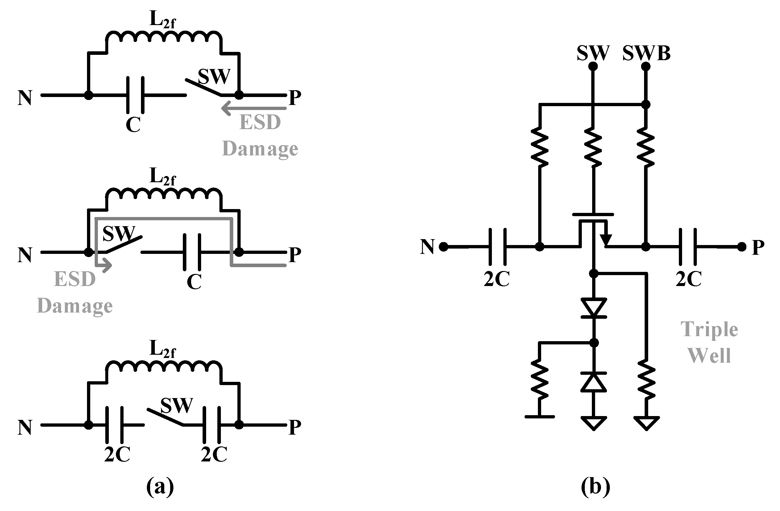
The proposed CMCD PA has two switched
capacitors. One is the primary resonant capacitor of the XFMR, and the other is
for the HD2 rejection filter. Since the CMCD PA is a differential circuit, the
switched capacitors must also be differential, which uses two 2X capacitors in
series compared to a single-ended structure. For the HD2 rejection filter,
since it is a single-ended filter, a single-ended switch capacitor structure
can be applied. However, a differential structure should also be used for the
HD2 rejection filter because in a single-ended structure, the switch nMOSFETs
are directly connected to the PAD, making them vulnerable to ESD damage as
shown in
Figure 8(a). In the differential
configuration, there is no direct current path from the PAD. The differential
configuration uses the triple-well that helps float the device's body voltage
to prevent junction failures due to potentially large swings across all nodes
of the switch as shown in
Figure 8(b).
Similarly, the gate, drain, and source nodes are also floated while being
DC-biased through large resistors. A large resistor of 20 kΩ is chosen to
minimize the insertion loss of the switch. When the switch is on, the source
and drain node DC voltages are pulled to GND. When the switch is off, the source
and drain node DC voltages are pulled to VDD. This prevents the junction from
being biased forward due to the swing seen on the other port after the switch
is turned on, potentially degrading linearity or gain.
3.4. HD2 Suppression with Duty-Cycle Correction
Differential PA topologies are commonly
used to suppress HD2 emissions, which can violate spurious emission limits in
wireless standards. However, its effectiveness is limited by device mismatch
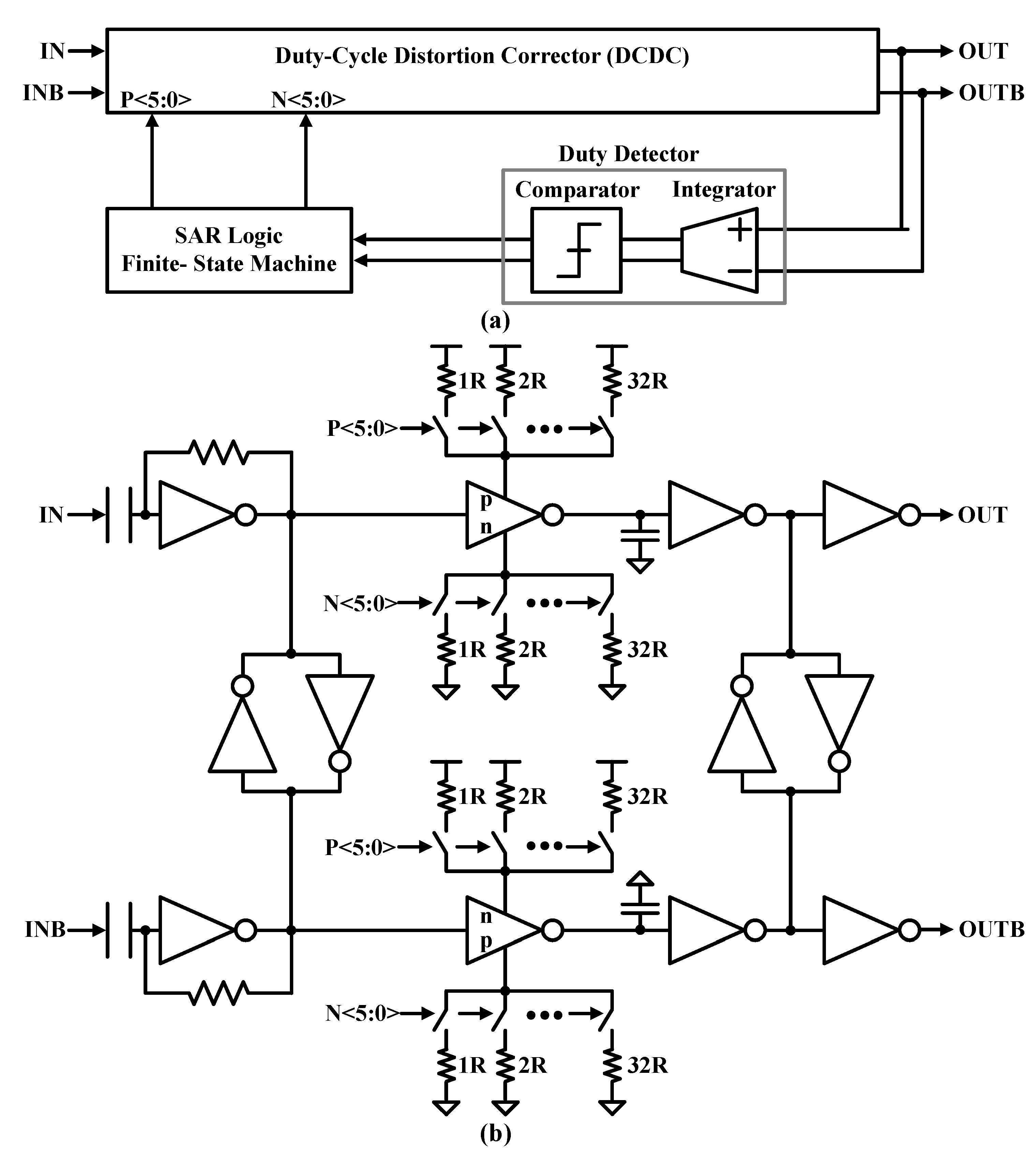
and asymmetry. The HD2 is caused by the input data duty cycle imbalance, so the
proposed TX employes a duty cycle correction circuit (DCC) before driving the
CMCD PA.
Figure 9(a) shows the block
diagram of the successive approximation register (SAR)-DCC circuit, which
consists of a duty-cycle distortion corrector (DCDC), a duty-cycle detector
(DCD), and a SAR logic controller. The DCD essentially consists of an analog
integrator and a comparator. The integrator is a fully differential charge pump
with a common-mode feedback circuit, and the fully differential dynamic
comparator is based on two cross-coupled differential pairs with switched
current sources loaded with a CMOS latch. The output of the comparator is given
to the SAR logic controller that adopts the binary search algorithm and adjusts
load capacitances in the DCDC to correct the input duty cycle by 50%. The
duty-cycle error correction loop is continuously running to compensate for
voltage and temperature drift. A 10 MHz clock is used to run the error
detection and correction logic.
Figure 9(b)
shows the digitally controlled DCDC circuit. The first stage of the DCDC, an
AC-coupled resistive feedback inverter, compensates for the duty cycle error to
some extent on its own. This is done by storing the average value of the input
in an AC capacitor. Change the common-mode voltage at the input of the
first-stage inverter. The DCDC calibration is performed down to 1.5 ns with a
resolution of up to ±45 ns in the time domain by the digital control words
P<5:0> and N<5:0>, which independently adjusts the pull-up and
pull-down resistors of the delay device. This corresponds to a correction
operation of ±32 degrees in the phase domain, with a resolution of
approximately 0.5 degrees at a data rate of 2 Mb/s.
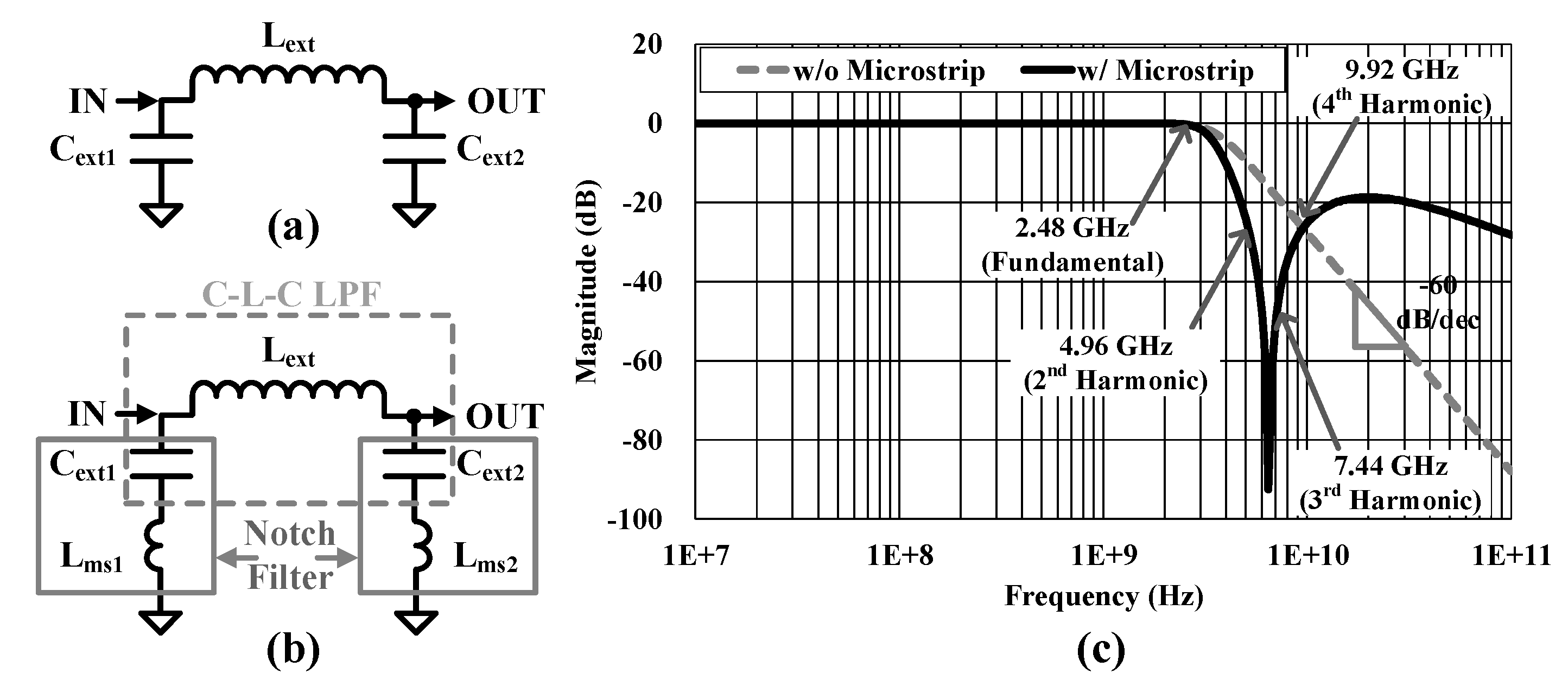
3.5. External CLC Low-Pass-Filter for Harmonic Suppression
An external C-L-C filter consisting of a
capacitor-inductor-capacitor in a π configuration creates a low-pass filter
(LPF) for harmonics suppression as shown in
Figure 10(a). The input capacitor (C
ext1) effectively filters the
CMCD PA switching harmonics and helps to reduce the capacity and size of each
component. The C
ext1 provides very low reactance to the ripple
frequency, so the main part of the filtering is done by C
ext1. Most
of the residual ripple is removed by the combined effect of L
ext and
C
ext2. The C-L-C filter contains three L or C elements. Hence, the
filter is essentially a third-order filter and provides -60 dB/decade of
roll-off at frequencies above a cutoff frequency of
, where C
ext is 1 pF, the same
as C
ext1 and C
ext2, and L
ext is 4 nH. However,
it only provides HD2 suppression of 9 dB as the second harmonic frequency is
close to the fundamental frequency as shown in
Figure 10(c).
Microstrip inductance of 600 pH is added
between C
ext to GND path on a printed circuit board (PCB), which can
add two notch filters in addition to C-L-C LPF as shown in
Figure 10(b). The resonance frequency of the
notch filters is 6.5 GHz which is between the second and third harmonic
frequency, and it gives HD2 suppression of 23 dB and HD3 suppression of 42 dB.
The suppression is much higher than the simple C-L-C LPF. They have the same
HD4 suppression. Harmonic components of greater than HD4 are lesser than the
regulatory limit of -41.2 dBm without the external filter.
4. Experimental Results
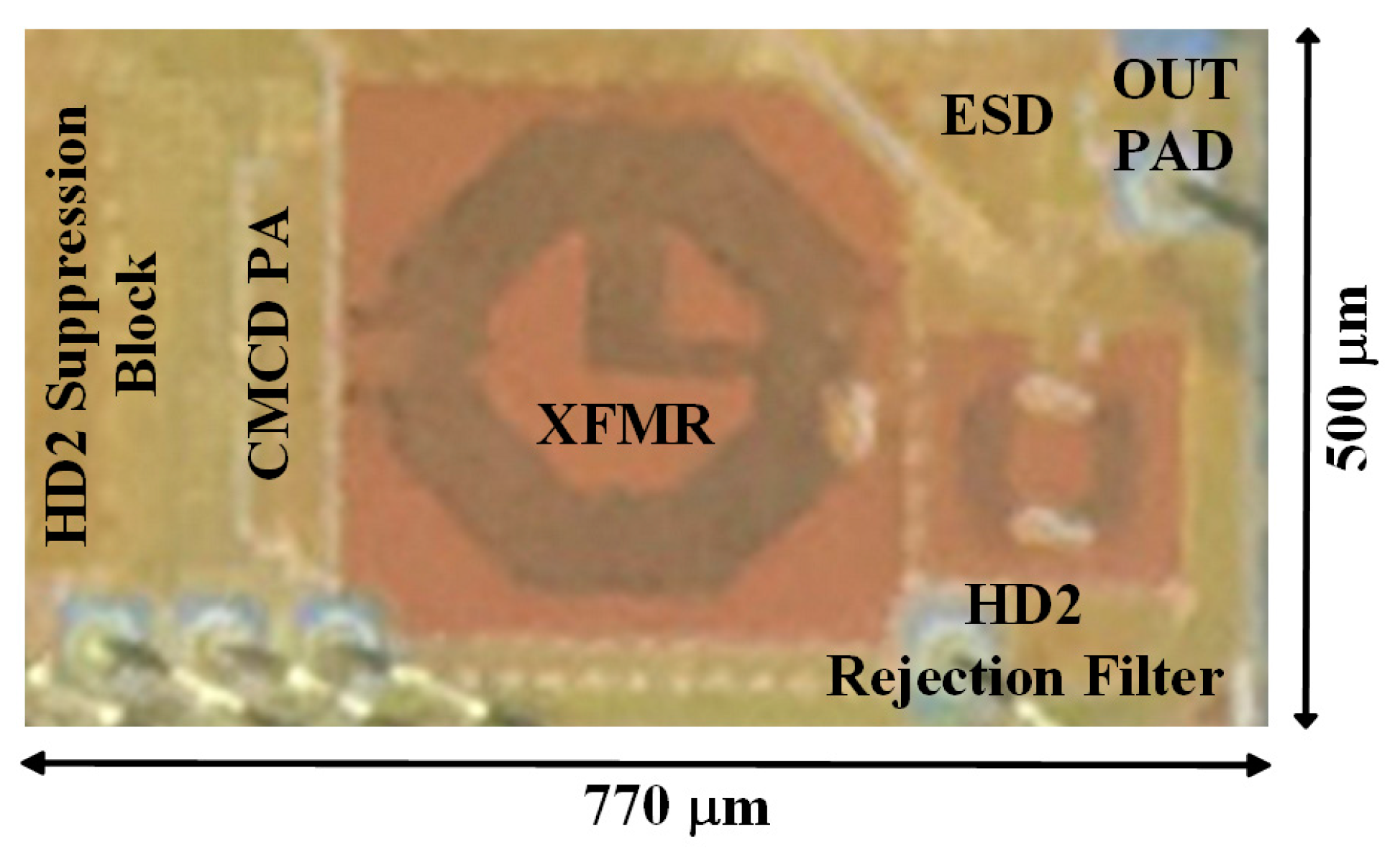
Figure 11
shows a micrograph of the proposed TX implemented in a 1P8M 28-nm CMOS process.
It includes the HD2 suppression block, the CMCD PA, the XFMR, the HD2 rejection
filter, the ESD diodes on the die, and input/output PADs. The die area is 0.385
mm
2. The C-L-C LPF is attached to the
output PAD on the PCB.
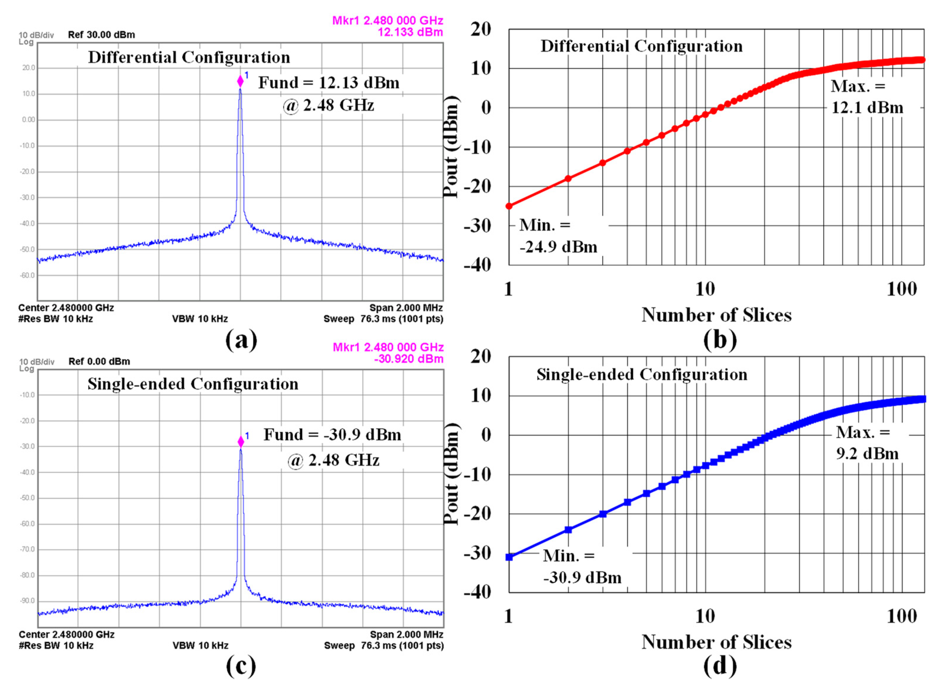
The maximum output power of the
differential CMCD PA is 12.13 dBm for unmodulated data as shown in
Figure 12(a). In addition, the PA can be
digitally tuned between -24.9 and +12.1 dBm by changing the number of slices
from 1 to 127 as shown in
Figure 12(b).
The proposed PA also offers a single-ended configuration with a minimum output
power of -30.9 dBm for unmodulated data as shown in
Figure 12(c). Figure
12(d) shows digitally controllable output powers from -30.9 to 9.2 dBm
by varying the number of slices from 1 to 127 for the single-ended
configuration. Thus, different output power levels can be achieved by mixing
differential and single-ended configurations.
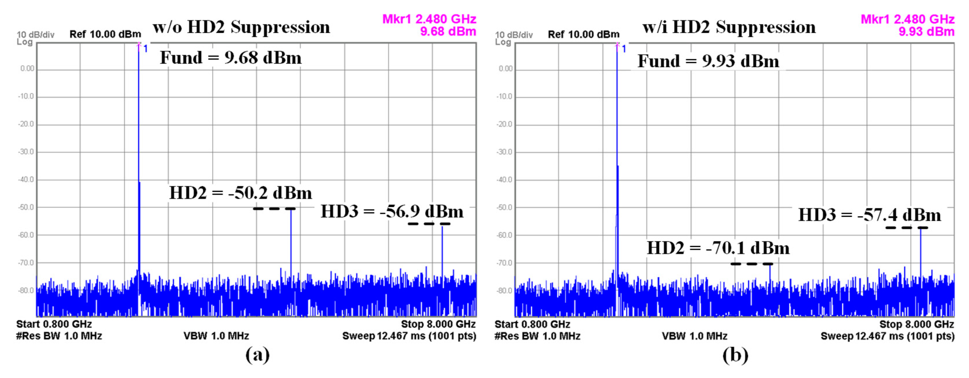
Figure 13
shows the TX harmonic suppression performance at the maximum free frequency
channel of 2.48 GHz with and without HD2 suppression using duty cycle
distortion correction. Under the +9.68 dBm output power condition without duty
cycle correction, the harmonic level of HD2 is -50.2 dBm and HD3 exhibits -56.9
dBm as shown in
Figure 13(a). The
harmonic levels can meet the regulatory limit of -41.2 dBm with the help of the
HD2 rejection filter and modified C-L-C LPF filter. After enabling duty cycle
correction for HD2 suppression, the fundamental output power is +9.93 dBm, the
HD2 level decreases to -70.1 dBm, and the HD3 level achieves -57.4 dBm as shown
in
Figure 13(b). Thus, the HD2
suppression function block is found to improve the HD2 level by 20.2 dB.
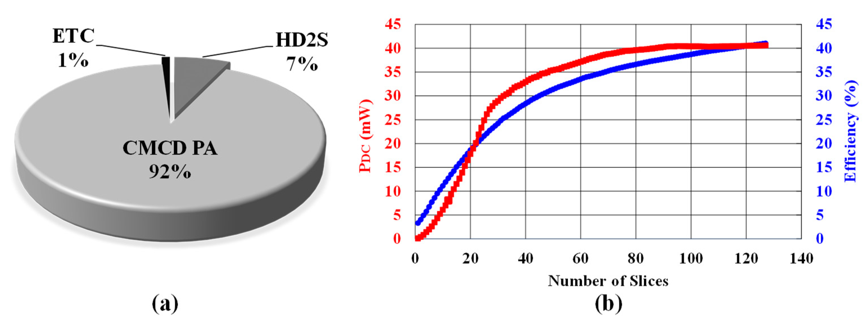
Figure 14a)
shows the measured power breakdown of the proposed TX. Under the +12.1 dBm output
power condition at 2.48 GHz, the TX consumes 41 mW of DC power (P
DC).
Among the total power consumption, the CMCD PA consumes 92% and the HD2
suppression block consumes only 7% of the total power.
Figure 14(b) shows the DC power (P
DC)
taken from the supply and efficiency that is defined by output power (P
OUT)/P
DC
in percentage as a function of the number of slices from 1 to 127. The input
signal is a 500-mV peak-to-peak sinusoidal wave. The minimum power consumption
is 3.2 mW at -25 dBm P
OUT with differential configuration. The
maximum efficiency is 40.6% at +12.1 dBm P
OUT.
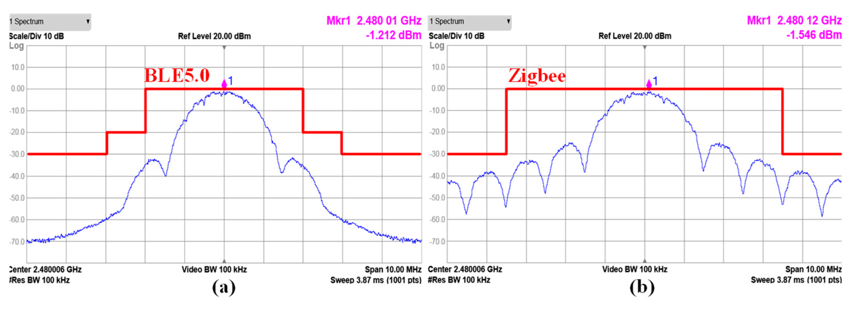
Figure 15
shows the TX spectrums of the 2 Mb/s data rate Gaussian frequency-shift keying
(GFSK) modulation for the BLE mode and of the 256 kb/s data rate offset
quadrature phase shift keying (O-QPSK) modulation for Zigbee mode. The
modulated output spectrums are measured with the maximum P
OUT
setting and a 2
31 − 1 pseudorandom binary sequence (PRBS). The
spectrum for the GFSK modulation has a 14-dB margin from the BLE spectral mask,
and the O-QPSK modulation has an 8-dB margin from the Zigbee spectral mask.
The performance of this work is summarized
and benchmarked against state-of-the-art TXs operating at the 2.4 GHz ISM band
for IoT applications [
7,
8,
10,
11,
13,
14,
15,
20] in
Table I. The proposed TX achieves the highest and the lowest P
OUT
which guarantees the widest range of the P
OUT. Moreover, HD2 of
-82.2 dBc is the lowest level compared to the previous works. The maximum TX
efficiency, defined as a percentage by P
OUT,MAX/P
DC,MAX,
is 39.8%, which ranks second compared to the previous works due to the many
slices of the 7-bit programmable CMCD PA. The transmitter figure-of-merit
(TX_FoM) [
21] is applied for the fair
comparison to account for HD2 rejection performance under limited power consumption
and is defined by equation (3) in dB. The proposed TX ensures the best TX_FoM
thanks to the lowest HD2 level by HD2 compression block, HD2 rejection filter,
and modified C-L-C filter.
5. Conclusions
The high-efficiency wide-range transmitter
using the digitally controlled CMOS current-mode Class-D switching PA is
demonstrated in a 28 nm CMOS technology with an area of 0.39 mm2. The wide
range is achieved by using a mix of differential and single-ended
configurations. With the current-domain operation, CMCD PAs can impose
zero-voltage switching conditions to mitigate parasitic discharge issues and
are suitable for high-power applications with superior efficiency compared to
Class E/F PAs. The on-chip XFMR baluns at the output of the PA provide
impedance matching along with a low-loss TX switch. The TX maintains
sufficiently high HD2 suppression utilizing the proposed duty-cycle distortion
correction in addition to the HD2 rejection filter and the modified C-L-C LPF.
The proposed TX provides a wide range of power from -31 to 12.1 dBm and
achieves an efficiency of 39.8 % at maximum output power while consuming 41.1
mW. The suppressed HD2 level is -82.2 dBc at an output power of 9.93 dBm,
resulting in an excellent TX_FoM of -97.52 dB. With full on-chip integration
and high efficiency, the TX complies with BLE and Zigbee requirements, enabling
long-life IoT sensor nodes that ubiquitously support wireless personal area
networks (WPANs) and wireless body area networks (WBANs).
Funding
This research was supported by the Institute of Information & communications Technology Planning & Evaluation (IITP) grant funded by MSIT of Korea government under grant number RS-2023-00229689. This research was supported by Chungbuk National University BK21 program(2021). The EDA tool was supported by the Integrated Circuit Design Education Center (IDEC), Korea.
Institutional Review Board Statement
Not applicable.
Informed Consent Statement
Not applicable.
Data Availability Statement
Not applicable.
Conflicts of Interest
The authors declare no conflict of interest. The funders had no role in the design of the study; in the collection, analyses, or interpretation of data; in the writing of the manuscript, or in the decision to publish the results.
References
- Akyildiz, I.F.; Su, W.; Sankarasubramaniam, Y.; Cayirci, E. Wireless Sensor Networks: A Survey. Comput. Netw. 2002, 38, 399–422. [Google Scholar] [CrossRef]
- Brito, T.; Pereira, A.I.; Lima, J. ; Valente, A Wireless Sensor Network for Ignitions Detection: An IoT approach. Electronics 2020, 9, 893. [Google Scholar] [CrossRef]
- Basu, D.; Moretti, G.; Gupta, G.S.; Marsland, S. Wireless sensor network based smart home: Sensor selection, deployment and monitoring. In Proceedings of the IEEE Sensors Applications Symposium Proceedings, Galveston, TX, USA, 19–21 February 2013; pp. 49–54. [Google Scholar]
- Latha, R.; Vetrivelan, P. Wireless Body Area Network (WBAN)-Based Telemedicine for Emergency Care. Sensors 2020, 20, 2153. [Google Scholar] [CrossRef]
- Kuo, F.; Binsfeld Ferreira, S.; Chen, H.R.; Cho, L.; Jou, C.; Hsueh, F.; Madadi, I.; Tohidian, M.; Shahmohammadi, M.; Babaie, M.; et al. A Bluetooth Low-Energy Transceiver with 3.7-mW All-Digital Transmitter, 2.75-mW High-IF Discrete-Time Receiver, and TX/RX Switchable On-Chip Matching Network. IEEE J. Solid-State Circuits 2017, 52, 1144–1162. [Google Scholar] [CrossRef]
- Ding, M.; Zhang, P.; He, Y.; Traferro, S.; Song, M.; Korpela, H.; Shibata, K.; Ueda, K.; Liu, Y.-H.; Bachmann, C. A 3.9 mW Bluetooth Low-Energy Transmitter Using All-Digital PLL-Based Direct FSK Modulation in 55 nm CMOS. IEEE J. Solid State Circuits 2021, 56, 254–266. [Google Scholar] [CrossRef]
- Huang, H.; Liu, X.; Tang, Z.; Song, W.; Zhang, Y.; Ma, X.; Zhang, M.; Wang, J.; Wang, Z.; Li, G. A 2 nJ/bit, 2.3% FSK Error Fully Integrated Sub-2.4 GHz Transmitter With Duty-Cycle Controlled PA for Medical Band. IEEE Trans. Circuits Syst. I Reg. Pap. 2022, 69, 5018–5029. [Google Scholar] [CrossRef]
- Yang, W.; Hu, D.Y.; Lam, C.K.; Cui, J.Q.; Soh, L.K.; Song, D.C.; Zhong, X.W.; Hor, H.C.; Heng, C.L. A +8 dBm BLE/BT Transceiver with Automatically Calibrated Integrated RF Bandpass Filter and −58 dBc TX HD2. In Proceedings of the IEEE International Solid-State Circuits Conference—Digest of Technical Papers, San Francisco, CA, USA, 11–15 February 2017; pp. 136–137. [Google Scholar]
- Aksin, D.; Gregori, S.; Maloberti, F. High-efficiency power amplifier for wireless sensor networks. In Proceedings of the IEEE International Symposium on Circuits and Systems, ISCAS 2005, Kobe, Japan, 23–26 May 2005; pp. 5898–5901. [Google Scholar]
- Sharifzadeh, M.; Masnadi-Shirazi, A.H.; Rajavi, Y.; Lavasani, H.M.; Taghivand, M. A fully integrated multi-mode high-efficiency transmitter for IoT applications in 40 nm CMOS. In Proceedings of the IEEE Custom Integr. Circuits Conf. (CICC), San Diego, USA, 8-10 Apr. 2018; pp. 1–4. [Google Scholar]
- Oh, S.; Kim, S.; Ali, I.; Nga, T.T.K.; Lee, D.; Pu, Y.; Yoo, S.-S.; Lee, M.; Hwang, K.C.; Yang, Y.; et al. A 3.9 mW Bluetooth Low-Energy Transmitter Using All-Digital PLL-Based Direct FSK Modulation in 55 nm CMOS. IEEE Trans. Circuits Syst. I Reg. Pap. 2018, 65, 3037–3048. [Google Scholar] [CrossRef]
- Kobayashi, H.; Hinrichs, J.M.; Asbeck, P.M. Current-mode class-D power amplifiers for high-efficiency RF applications. IEEE Trans. Microw. Theory Tech. 2001, 49, 2480–2485. [Google Scholar] [CrossRef]
- Prummel, J.; Papamichail, M.; Seesink, P.; Willms, J.; Todi, R.; Aartsen, W.; Kruiskamp, W.; Haanstra, J.; Opbroek, E.; Rievers, S.; Babaie, M.; Kuo, F.W.; Chen, H.N.R.; Cho, L.C.; Jou, C.P.; Hsueh, F.L.; Shahmohammadi, M.; Staszewski, R.B. A Fully Integrated Bluetooth Low-Energy Transmitter in 28 Nm CMOS With 36% System Efficiency at 3 DBm. IEEE J. Solid-State Circuits 2016, 51, 1547–1565, et al. A 10mW Bluetooth Low‐Energy transceiver with on‐chip matching. IEEE J. Solid State Circuits 2015, 50, 3077–3088. [Google Scholar]
- Sun, Z.; Liu, H.; Huang, H.; Tang, D.; Xu, D.; Kaneko, T.; Li, Z.; Pang, J.; Wu, R.; Okada, K.; et al. A 0.85 mm2 BLE Transceiver Using an On-Chip Harmonic-Suppressed RFIO Circuitry With T/R Switch. IEEE Trans. Circuits Syst. I Regul. Pap. 2021, 68, 196–209. [Google Scholar] [CrossRef]
- Babaie, M.; Kuo, F.W.; Chen, H.N.R.; Cho, L.C.; Jou, C.P.; Hsueh, F.L.; Shahmohammadi, M.; Staszewski, R.B. A Fully Integrated Bluetooth Low-Energy Transmitter in 28 Nm CMOS With 36% System Efficiency at 3 DBm. IEEE J. Solid-State Circuits 2016, 51, 1547–1565. [Google Scholar] [CrossRef]
- Kearney, N.; et al. 26.4 a 160-to-960 MHz ETSI class-1-compliant IoE transceiver with 100 dB blocker rejection, 70dB ACR and 800 pA standby current. In IEEE Int. Solid-State Circuits Conf. (ISSCC) Dig. Tech. Papers; 2016; pp. 442–443. [Google Scholar]
- Miyashita, D.; Ishikuro, H.; Shimada, T.; Tanzawa, T.; Kousai, S.; Kobayashi, H.; Majima, H.; Agawa, K.; Hamada, M.; Hatori, F. A low-IF CMOS single-chip Bluetooth EDR transmitter with digital I/Q mismatch trimming circuit. In Proceedings of the 2016 IEEE Symposium on VLSI Technology, Kyoto, Japan, 16–18 June 2005; IEEE: Piscataway, NJ, USA, 2016; pp. 298–301. [Google Scholar]
- Srimuang PPuangngernmak NChalermwisutkul, S. 13.56 MHz class E power amplifier with 94.6% efficiency and 31 watts output power for RF heating applications. 2014 11th International Conference on Electrical Engineering/Electronics, Computer, Telecommunications and Information Technology, Nakhon Ratchasima: Thailand, 2014; pp. 1–5. [Google Scholar]
- Kobayashi, H.; Hinrichs, J.M.; Asbeck, P.M. Current-mode class-D power amplifiers for high-efficiency RF applications. IEEE Trans. Microw. Theory Tech. 2001, 49, 2480–2485. [Google Scholar] [CrossRef]
- Kim, S.J.; Kim, D.G.; Oh, S.J.; Lee, D.S.; Pu, Y.G.; Hwang, K.C.; Yang, Y.; Lee, K.Y. A Fully Integrated Bluetooth Low-Energy Transceiver with Integrated Single Pole Double Throw and Power Management Unit for IoT Sensors. Sensors 2019, 19, 2420. [Google Scholar] [CrossRef] [PubMed]
- Sano, T.; Mizokami, M.; Matsui, H.; Ueda, K.; Shibata, K.; Toyota, K.; Saitou, T.; Sato, H.; Yahagi, K.; Hayashi, Y. 13. In 4 A 6.3 mW BLE transceiver embedded RX image-rejection filter and TX harmonic-suppression filter reusing on-chip matching network. In Proceedings of the IEEE International Solid-State Circuits Conference (ISSCC), San Francisco, CA, USA, 22–26 February 2015; pp. 1–3. [Google Scholar]
Figure 1.
WBAN and WPAN for wireless sensor networks.
Figure 1.
WBAN and WPAN for wireless sensor networks.
Figure 2.
(a) electromagnetic compatibility and (b) harmonic spurious emission regulation of BLE and (c) oscillator pulling due to high power outputs of the PA.
Figure 2.
(a) electromagnetic compatibility and (b) harmonic spurious emission regulation of BLE and (c) oscillator pulling due to high power outputs of the PA.
Figure 3.
(a) Voltage mode class-D PA (VMCD) and (b) current mode class D PA (CMCD).
Figure 3.
(a) Voltage mode class-D PA (VMCD) and (b) current mode class D PA (CMCD).
Figure 4.
Proposed transmitter architecture block diagram.
Figure 4.
Proposed transmitter architecture block diagram.
Figure 5.
(a) Wide-range CMCD PA, (b) AND gate, and (c) differential and (d) single-ended CMCD.
Figure 5.
(a) Wide-range CMCD PA, (b) AND gate, and (c) differential and (d) single-ended CMCD.
Figure 6.
(a) XFMR and inductor of HD2 rejection filter and (b) their equivalent circuit.
Figure 6.
(a) XFMR and inductor of HD2 rejection filter and (b) their equivalent circuit.
Figure 7.
Embedded low-loss TX switch for RX operation mode.
Figure 7.
Embedded low-loss TX switch for RX operation mode.
Figure 8.
(a) Single-ended and differential switched capacitor scheme for HD2 rejection filter and (b) differential switched capacitor configuration using triple-well.
Figure 8.
(a) Single-ended and differential switched capacitor scheme for HD2 rejection filter and (b) differential switched capacitor configuration using triple-well.
Figure 9.
(a) HD2 suppression block diagram and (b) digitally controlled DCDC circuit.
Figure 9.
(a) HD2 suppression block diagram and (b) digitally controlled DCDC circuit.
Figure 10.
(a) C-L-C LPF, (b) modified C-L-C having microstrip inductance LPF, and (c) their magnitude frequency response.
Figure 10.
(a) C-L-C LPF, (b) modified C-L-C having microstrip inductance LPF, and (c) their magnitude frequency response.
Figure 11.
Microphotograph of the proposed transmitter.
Figure 11.
Microphotograph of the proposed transmitter.
Figure 12.
(a) The measured maximum output power of the differential CMCD PA, (b) its output power as a function of the number of slices, (c) the measured minimum output power of the single-ended CMCD PA, and (d) its output power as a function of the number of slices.
Figure 12.
(a) The measured maximum output power of the differential CMCD PA, (b) its output power as a function of the number of slices, (c) the measured minimum output power of the single-ended CMCD PA, and (d) its output power as a function of the number of slices.
Figure 13.
Measured TX typical harmonic: (a) without and (b) with HD2 suppression.
Figure 13.
Measured TX typical harmonic: (a) without and (b) with HD2 suppression.
Figure 14.
(a) Breakdown of measured TX power consumption and (b) DC power (PDC) and efficiency as a function of the number of slices.
Figure 14.
(a) Breakdown of measured TX power consumption and (b) DC power (PDC) and efficiency as a function of the number of slices.
Figure 15.
Measured TX spectrum (a) at 2 Mb/s for BLE5.0 and (b) at 256 kb/s for Zigbee.
Figure 15.
Measured TX spectrum (a) at 2 Mb/s for BLE5.0 and (b) at 256 kb/s for Zigbee.
Table 1.
Performance summary of the proposed TX and comparisons with the state-of-the arts.
Table 1.
Performance summary of the proposed TX and comparisons with the state-of-the arts.
| |
This
Work |
[7] TCAS-I 2022 |
[8] ISSCC 2017 |
[10] CICC 2018 |
[11] TCAS -I 2018 |
[13] JSSC 2015 |
[14] TCAS
-I 2021 |
[15] JSSC 2016 |
[20] Sensors 2019 |
CMOS
Technology (nm)
|
28 |
40 |
55 |
40 |
55 |
55 |
65 |
28 |
55 |
Supply
Voltage (V)
|
1.0 |
1.1 |
1.2 |
1.1 |
3 |
3.3 |
0.6 |
3 |
3.3 |
| PA Topology |
Class-D |
Class-E |
Class-AB |
Class-D |
Class-D |
Class-D |
Class-E/F2 |
Class-E/F2 |
Class-D |
| Area (mm2) |
0.39 |
0.48 |
2.2* |
0.7 |
0.53 |
N/A |
0.7 |
0.65 |
2.9* |
| TX max POUT (dBm) |
12.1 |
0 |
8 |
4 |
10.05 |
0 |
0 |
3 |
-0.39 |
| TX min POUT (dBm) |
-31 |
-10 |
N/A |
-10 |
-23 |
-20 |
N/A |
-5 |
N/A |
HD2 (dBc)
@ TX POUT
|
-82.2
@ +9.93
|
-41.3
@ -3 |
-58
@ +8 |
-52
@ 0 |
-45.6
@ +1.6 |
-54
@ 0 |
-58
@ 0 |
-50
@ 0 |
-50.07
@ -0.39 |
HD3 (dBc)
@ TX POUT
|
-67.3
@ +9.93 |
-54.2
@ -3 |
-64
@ +8 |
-30
@ 0 |
-50.6
@ +1.6 |
N/A |
-64
@ 0 |
-47
@ 0 |
-47.08
@ -0.39 |
Max. PDC (mW)
@ TX POUT
|
41.1
@ +12.1 |
4.85
@ 0 |
79.8
@ +8 |
N/A |
18
@ +10 |
10.1
@ 0 |
5.4
@ 0 |
6.3
@ +3 |
6
@ -0.39 |
Max. TX
Efficiency (%)
@ TX POUT
|
39.8
@ +12.1 |
20.6
@ 0 |
7.9
@ +8 |
N/A |
55.6
@ +10 |
9.9
@ 0 |
18.5
@ 0 |
31.7
@ +3 |
15.2
@ -0.39 |
PDC (mW)
@ TX POUT
|
29.4
@ +9.93 |
3.22
@ -3 |
N/A |
4.5
@ 0 |
3.9
@ +1.6 |
N/A |
N/A |
4.4
@ 0 |
N/A |
TX Efficiency (%)
@ TX POUT
|
33.5
@ +9.93 |
15.6
@ -3 |
N/A |
22.2
@ 0 |
37.1
@ +1.6 |
N/A |
N/A |
22.7
@ 0 |
N/A |
TX_FoM (dB)
@ TX POUT
|
-97.52
@ +9.93
|
-66.52
@ -3 |
-68.99
@ -3 |
-75.47
@ 0 |
-69.69
@ +1.6 |
-73.96
@ 0 |
-80.68
@ 0 |
-73.57
@ 0 |
-72.29
@ -0.39 |
|
Disclaimer/Publisher’s Note: The statements, opinions and data contained in all publications are solely those of the individual author(s) and contributor(s) and not of MDPI and/or the editor(s). MDPI and/or the editor(s) disclaim responsibility for any injury to people or property resulting from any ideas, methods, instructions or products referred to in the content. |
© 2024 by the authors. Licensee MDPI, Basel, Switzerland. This article is an open access article distributed under the terms and conditions of the Creative Commons Attribution (CC BY) license (http://creativecommons.org/licenses/by/4.0/).
