1. Introduction
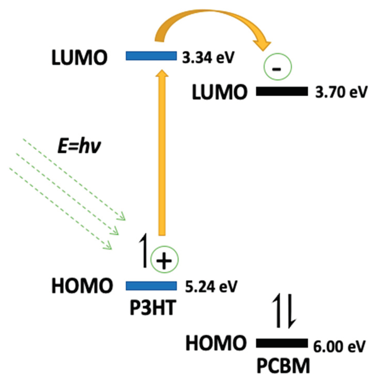
Photo doping is a photo induced charge separation process at a donor/acceptor interface as depicted schematically in
Figure 1, where a photon can be captured by an electron in donor which is excited from donor HOMO to the donor LUMO forming a Frenkel type of electron-hole pair or exciton [
1,
2,
3,
4]. The Frenkel exciton can then diffuses via energy transfer to a nearby donor/acceptor interface at where it is dissociated into electron at the acceptor and a hole at the donor by a potential field due to the LUMO orbital offset (∆E
1) between the donor and the acceptor, and that the electron transfers from the donor LUMO to the acceptor LUMO, and the hole remains in the donor HOMO [
2]. After the exciton dissociation and the electrons/holes moving away from D/A interface, the charge separation or a voltage can be achieved [
1,
2]. A popular polymer based photo doping D/A pair is P3HT/PCBM whose chemical structures are shown in
Figure 2, and P3HT/PCBM pair based polymer solar cells have been widely studied and reported [
1,
3,
4,
5,
6]. Previous studies have found that P3HT’s chemical structural regio-regularity induced solid-state ordered packing or crystallinity result in one of best hole mobility (> 1.0 cm
2/Vs) among conjugated polymers with a strong visible light absorption down to 650 nm [
3,
4,
5,
6]. With the addition of a minority amount of photo doping acceptor phenyl-C
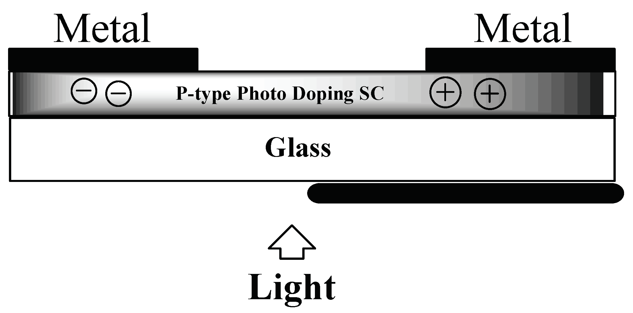
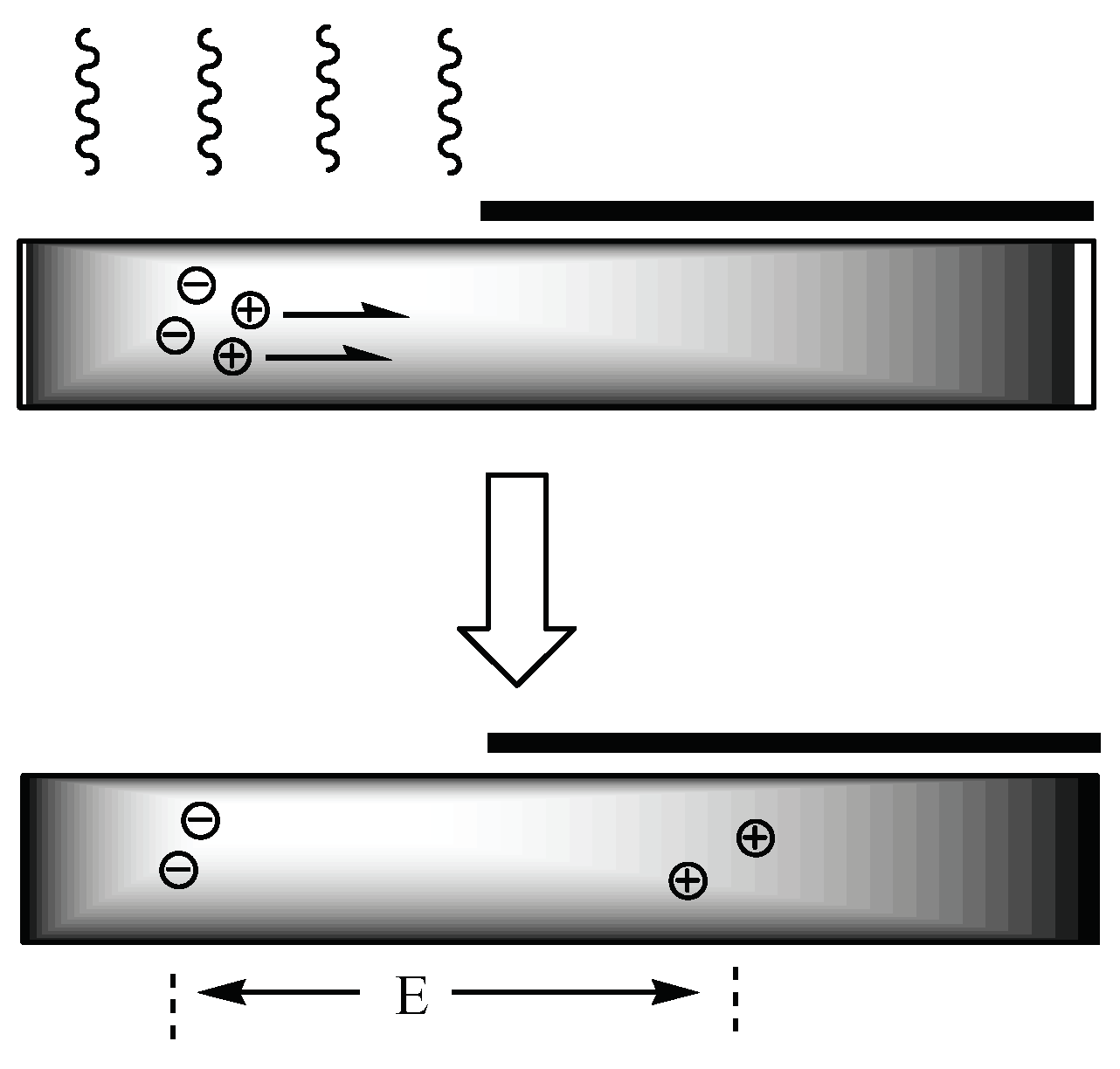
61-butyric acid methyl ester (PCBM), a p-type photo sensing device may be fabricated as schematically shown in
Figure 3, where a potential non-uniform illumination on left side generated mobile holes are diffusing toward right dark area via P3HT HOMOs, while the photo generated electrons are trapped in minority PCBM LUMOs on the left bright area, thus a photo generated voltage between the bright area and the dark area may be achieved. Previous studies of non-uniform illumination on photovoltaic cells have been mainly focused on analysis of solar cell conversion efficiencies of uniform versus non-uniform illuminations [
7,
8]. When P3HT/PCBM are equal amount mole ratio, then photo doping would yield equal amount of mobile electrons that can move in acceptor PCBM phase, and equal amount of mobile holes that can diffuse in donor P3HT phase, thus a solar cell can be realized between the positive ITO and negative Al electrodes (
Figure 4 and
Figure 5), or a photo conductor can be materialized between the same Al electrodes as show in
Figure 5 and
Figure 6.
Most or typical solar cells including P3HT/PCBM cells are fabricated with equal amount of donor/acceptor pair under uniform illumination mode,
i.e., light illuminate the whole cell surface area uniformly generating equal mobile electrons and holes followed by their separation and migration to corresponding electrodes [
1,
3,
4,
5,
6]. In this work, however, bright-dark non-uniform light illumination in a p-type P3HT/PCBM photo doping pair are being investigated for potential non-uniform photovoltage generation applications. As
Figure 3 shows, while photo generated immobile/minority electrons are trapped at PCBM LUMOs and cannot move, majority/mobile holes at P3HT HOMOs can diffuse from the higher density area (brighter areas) toward the lower density areas (darker areas) driven by at least the hole density gradients and potential temperature gradients. Such mobile charge diffusion would cease until the density gradient force is countered or balanced by the Columbic attraction force as a result of separated electrons and holes. This charge separation and voltage generation mechanism is very similar in principle to the charge separation and mobile charge diffusion resulting in voltage generation of the thermoelectric (TE) Seebeck effects [
9], except that the charge generation is due to light in the photo doping case, and is due to heat in thermoelectric case.
2. Experimental
Sample/solution preparations
Throughout this project, regio-regular poly(3-hexylthiophene-2,5-diyl) P3HT was used. P3HT is one of the most popular conjugated semiconducting polymers for organic electronics and optoelectronics [
1,
2,
3,
4,
5,
6]. Donor Regio-Regular Poly(3-hexylthiophene-2,5-diyl), RR-P3HT (Aldrich Catalog # 445703-1G, Mw=50k~100k), and acceptor ([6,6]-Phenyl C
xy butyric acid methyl ester, or PC
xyBM, xy=61. Aldrich Catalog # 684430-1G. MW=910.88) composite samples are prepared as shown in
Table 1. PCBM and related fullerene acceptors are popular acceptor of choice in organic optoelectronic devices due to their relatively high electron mobility, solubility or processability in certain organic solvents, and desirable frontier orbital levels that match the P3HT [
1,
3,
4,
5,
6]. All samples are dissolved in 1 mL o-Dichlorobenzene (DCB) each, and spun coated into thin films with typical 100-200 nm thickness.
Device glass substrate preparations
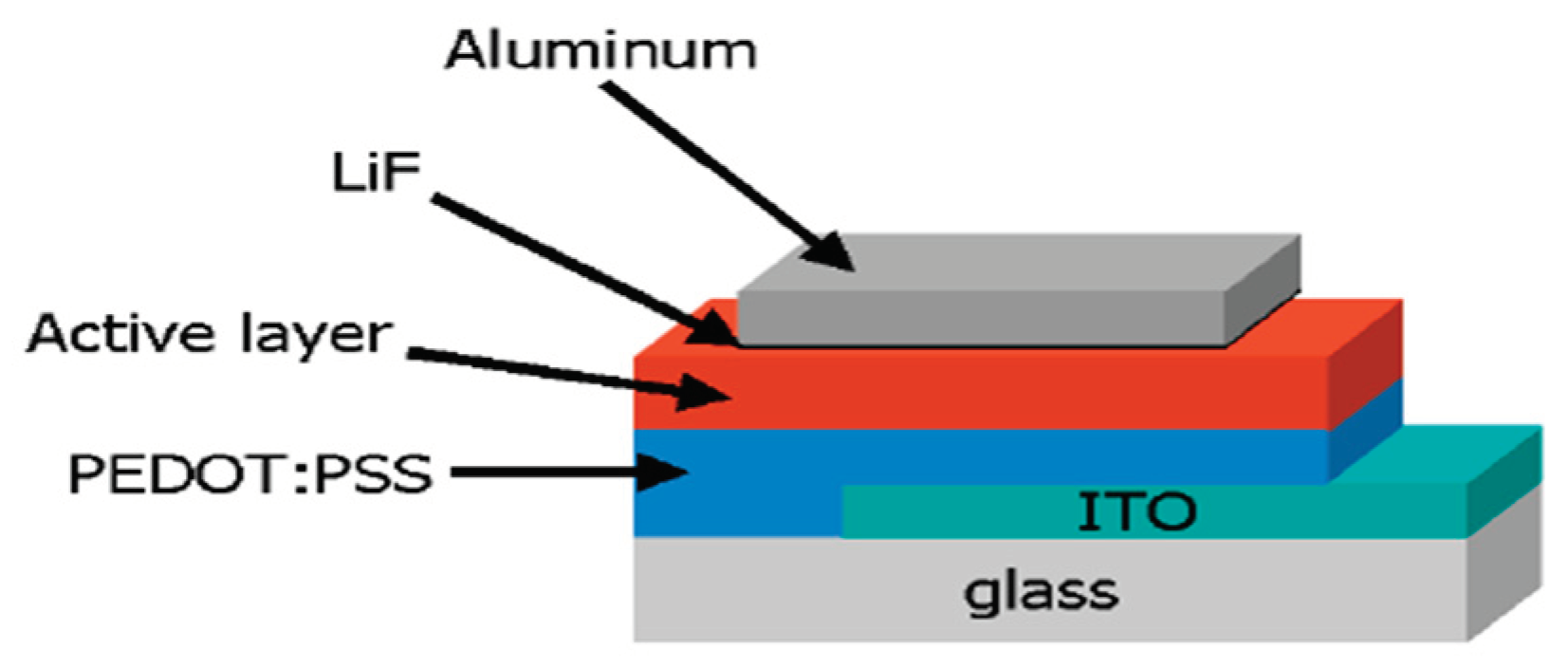
ITO glass vertical classic P3HT:PCBM PV cells: Cross section/side view scheme of classic P3HT:PCBM PV cells are shown in
Figure 4 (Note: A LiF and/or Ca thin layer between aluminum and organic active layer are helpful to improve electron collection at aluminum electrode but these layers are optional [
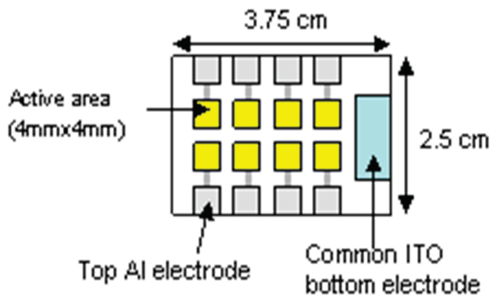
1]), and the top schematic view of the PV device is shown in
Figure 5 where eight PV cells (each cell active area 4mm x 4mm) are fabricated on a 25x37.5 mm ITO slide. Delta-Tech 25x75x0.4 mm ITO glass slides are used (5-100 Ohms resistance). The ITO side are detected using a Simpson electric multi-meter at Rx1 position (About 500 Ohms maximum). According to the cell pattern shown in
Figure 5, each original ITO slide is cut into two halves so each half slide has a size of 25x37.5 mm with eight cells fabricated on it (Figure 5). A scotch transparent tape strip is placed on top of the ITO side covering central two rows (yellow colored) of electrodes, the ITO areas on top and bottom two electrode rows (grey colored) are exposed without the tap. Taped ITO slides are then submerged into a
6M HCl solution for 10-20 min (or
concentrated 12M HCl solution for 3-5 min), or until the exposed ITO has been etched away as verified using the electric multi-meter. Etched ITO slides were then rinsed with DI water, and the tape immediately removed to avoid/minize the glue of the tape sticking to the ITO. Finaly the slides sonicated for five minutes each in 1) detergent; 2) DI water; 3) Acetone; 4) Isopropanol. (Note: To further improve the device efficiency, a plasma ion beam cleaning step can be utilized to give best results).
Figure 4.
Cross section/side view scheme of a classic P3HT:PCBM PV cell.
Figure 4.
Cross section/side view scheme of a classic P3HT:PCBM PV cell.
Figure 5.
Top view scheme of classical P3HT:PCBM PV cell device and electrodes mask illustration. Top row cells 1-4 are from left to right, bottom row cells 5-8 are from left to right.
Figure 5.
Top view scheme of classical P3HT:PCBM PV cell device and electrodes mask illustration. Top row cells 1-4 are from left to right, bottom row cells 5-8 are from left to right.
Figure 6.
Scheme of PV cell cross section/side view, where a light blocker underneath the glass can block one electrode from exposing to light, so the photo generated majority and mobile charges in the light exposed electrode area could difuse to the dark electrode area generating a voltage between two electrodes.
PEDOT:PSS coating
PEDOT:PSS aqueous solution (Clevious PVPAI 4083, from H.C. Starck) were spun coated onto above treated ITO slide surface via a 0.2 micron filter (See spin coating recipe #1 in
Table 3, typically include a key step of
5000 rpm for 30s, yielding about
30-50 nm thick PEDOT:PSS film on top of ITO slide).
Films were then heated at 120oC for 10 min on a heating plate to further remove the water residue in the PEDOT:PSS thin film, films were then heated at 80oC in a vacuum oven perferencially over night. Films were cooled down to room temperature, in preparation for the next coating.
Photo sensitive polymer coating
P3HT:PCBM polymer solutions prepared from
Table 1 are spun coated on top of dried “ITO/PEDOT:PSS” film at desired spin speed and time (using Spin Coating recipe #2 shown in
Table 4, including a step of
1000rpm-2000rpm for 30-120s to make desired film thickness, typically in a range of
100-200 nm. Too thick films would suffer from too high resistance, and too thin films would suffer from too low photon capture). Optimal thicknesses for P3HT:PCBM OPV’s range between 80-200nm [
3,
4,
5,
6].
After spin coating, all thin film samples were further themally annealed in vaccum oven at 130oC for 30 min to improve polymer morphology and overall performance. Visible light absorption red shift is observable after annealing of polymer thin films. Al electrodes are then added by means of evaporation in a vacuum evaporation chamber inside a glovebox.
I-V measurements
All device IV measurements were performed in a Braum inert gas glove box equipped with a solar simulator.
Classic P3HT:PCBM solar cell devices with equal amount each component would generate equal amount of electrons and holes upon photo radiation, and both electrons and holes are mobile and can diffuse to their respective electrodes (Al and ITO) via donor/acceptor phases, such materials are also called donor/acceptor bipolar type semiconductor composites [
10], and the charge transport is vertical or in Z-axis due to negative Al and positive ITO electrodes are at the top and bottom of the films.
The main objective of this work is to demonstrate photovoltage generation between light and dark areas under non-uniform light illumination. In the experiments, non uniform light illumination was achieved through the light blocking (via Al foils) of half the cell substrate preventing photo induced charges on that half resulting in an area of no or very low charge density area (
Figure 3 and
Figure 6), so a potential charge density differential can be formed between the light and dark area. The photovoltages (IV curves) were measured between the top in plain two Al electrodes while the device were under dark (expected to be insulating or very little leaking IV curve), under uniform light illumination (expected to be symmetric photo conductor/semiconductor), and under non-uniform light illumination (expected to be asymmetric photo semiconductor similar like a solar cell diode IV curve, if a photo induced charge density differential is indeed generated).
For classic P3HT:PCBM PV cell measurements (vertical or Z-direction IVs measurements between the positive ITO and negative Al electrodes) – a negative clip are connected onto each negative Al electrode from cell #1 to #8 and the positive electric clip are attached to the common ITO electrode (
Figure 5).
For the non-uniform light illumination measurements (measuring photovoltages in-plain between two Al electrodes as shown in
Figure 5 and
Figure 6) -we simply connect the negative electric clip onto each top cells #1 -4 electrodes and connect the positive electrode clip to the corresponding paired or bottom cells #5-8 electrodes! (
Figure 5). Uniform illumination refers both top and bottom electrodes are exposed to light, while non-uniform illumination refers to one electrode (bottom) is blocked from the light illumination.
3. Results and Discussions
Measurement system calibration: A commercially purchased silicon reference solar cell (ABET Technologies Inc., Device code: RK5N3726, Ref#: RR213KG5) was first measured, where an open circuit voltage (Voc=0.48 volt) and short circuit current (Isc = -10 mA) were obtained under our solar simulator. Both values are lower than the expected or specified values (Voc = 0.56 volt and Isc= -60 mA under 1.0 Sun) indicating our measurement system are under estimated, for instance, our light illumination intensity is much lower than one Sun (estimated at about 0.4 Sun). However, the system is good enough to characterize the photo cells with self comparison purpose.
Photo cell measurements: In pure or pristine P3HT (0% PCBM doping) film, due to photo generated Frenkel type excitons and there are no photoelectric charge separation, dark, uniform or non-uniform light illuminations are not expected to generate any charges or electrical voltages/currents, and indeed our measurements confirmed this for pristine P3HT cells. In about 100% PCBM doped sample (sample #7), due to both donor and acceptor are roughly equal, both photo generated electrons and holes can be mobile in its phase, both charges have the same density gradient and diffusion even if non-uniform light illuminations are applied, and therefore no asymmetric photo voltages (V
oc) are expected between the two in-plain Al electrodes. This was indeed confirmed in our sample cell #7 as it does not exhibit any asymmetric photo diode style IV curves under non-uniform illuminations. For p-type photo doing (PCBM doping levels between 0-90%), while in-plain measured uniform light illumination IV curves are expected to be higher than dark IV cures due to photo doping generated charges, asymmetric V
oc are not expected due to charge generaton symmetry in uniform illuminations. However, in non-uniform illuminations of two in plain Al electrode pairs, IV curves could exhibit asymmetric or non-zero V
oc due to charge density gradient between light and dark Al electrode area. Indeed,
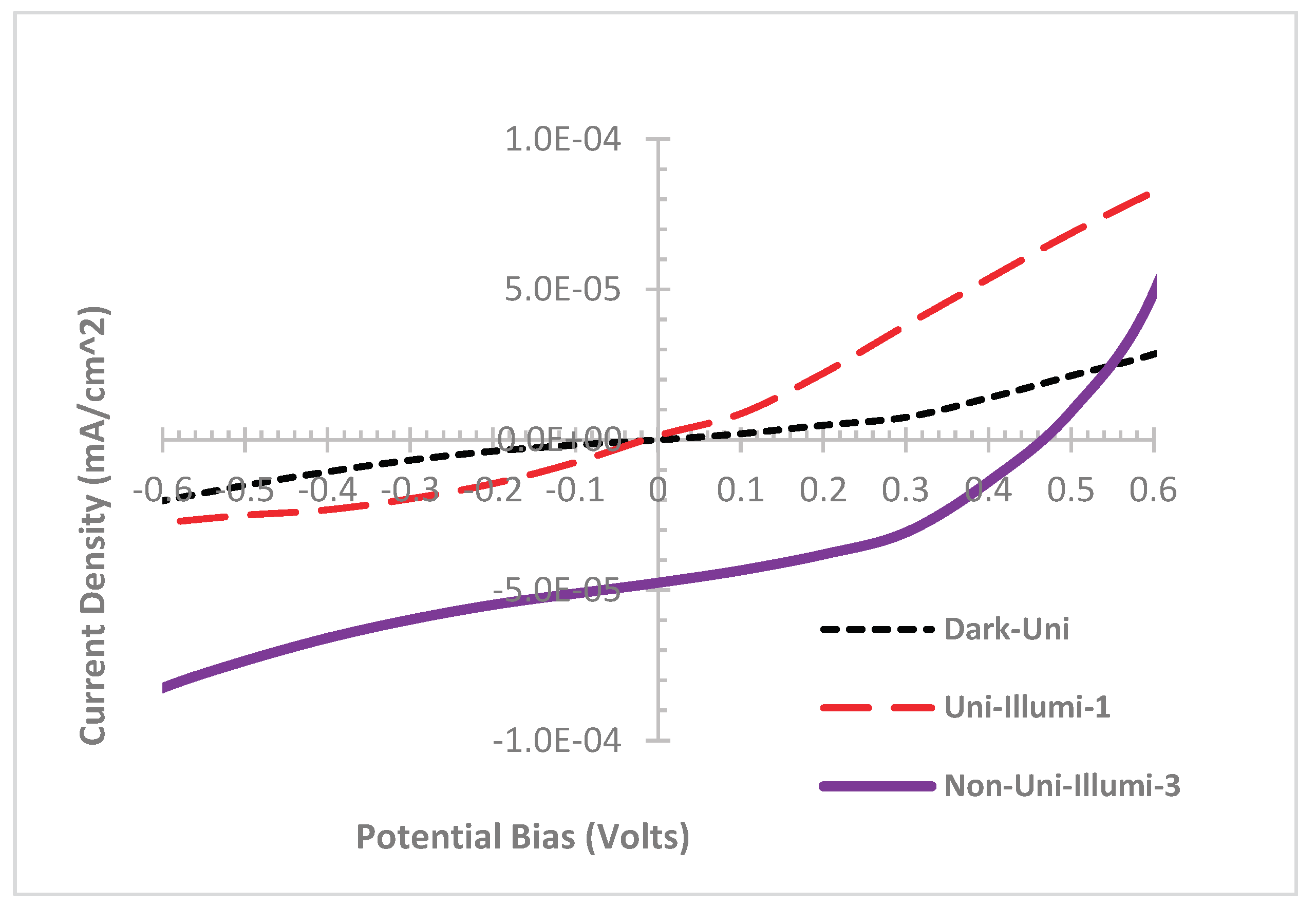
Figure 7 exhibits IV curves between two in plain Al electrode pair of sample #6 (about 80% PCBM doping ratio) with cell thickness of about 60 nm under dark (dark dashed line), under uniform light illumination (red long dashed line), and under non-uniform light illumination (Purple solid line). Uniform illumination current is higher than dark current can be explained by the photo doping generated charges (trapped electrons and mobile holes), however, the V
oc is zero due to both cells are exposed to the same light and the increased charge density are the same so there is no charge or voltage differential. When the bottom cell is blocked from light illumination and only top cell is exposed to light, the photo generated holes at top cell are diffused to the corresponding bottom cell while the electrons are being trapped at the top cell, thus a photo voltage (V
oc = 0.47 volt) between top and bottom cell are generated as shown in
Figure 7. To our knowledge, this is the first demonstration of photo voltage generated as a result of non-uniform illumination.
The term non uniform illumination here was coined to refer to subjecting a solar cell surface to bright and dark areas of illumination simultaneously, with the intention of generating a charge density gradient and a resulting photovoltage. Specifically, a polymeric composite thin film composed of P3HT (p-type photo doping semiconductor) and PCBM (photo doping electron acceptor) at varying p-type doping levels ranging from 0-100% were investigated in our studies. As
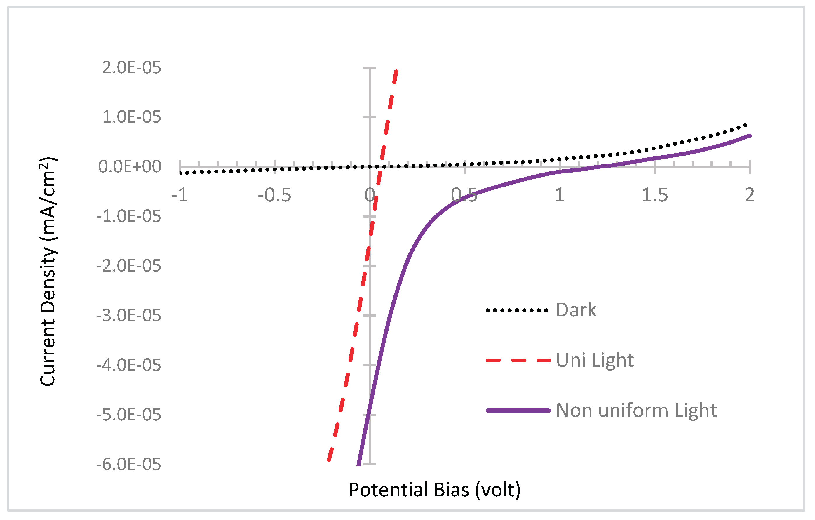
Table 1 exhibits, while non-uniform photovoltages for samples 1-5 (below 80% PCBM doing levels) were not obvious, sample/device #6 with about 80% PCBM doping level film of about 60 nm thick exhibited a 0.47 photovoltage under non-uniform illumination. Further experiments to repeat results of a 80% PCBM doping level at a thicker film of over 80nm also confirmed the symmetric photo conductive IV curves under uniform illumination, and asymmetric photo diode IV curves under non-uniform illuminations with a photovoltage between 1.2-1.3 volts observed as illustrated in
Figure 8. All cells are not optimized so IV curve shapes or fill factors are not optimal, as the main objective of this work is to demonstrate a non-uniform generated photovoltage.
When ITO layer was absent,
i.e., only P3HT:PCBM composite films were spun coated on top of the glass (with or without PSS:PEDOT layer), the non-uniform illumination photovoltages were not obvious or measurable between any in plain Al electrode. This implies, the ITO layer appears essential for the non-uniform light illumination generated photovoltages in the current device configuration. We hypothesis that, due to relatively high electrical resistance of P3HT [
10], photo generated mobile holes in the light area went vertically down to ITO layer and then transport directly and efficiently to the dark area through ITO and then move up vertically toward the dark area below Al electrode, as the resistivity is relatively small for P3HT film thickness of less than 100nm. However, with improvement of P3HT morphology and hole transport mobility, or with careful design of device geometries, it is possible that holes may be able to diffuse efficiently in plain from light area to dark area via P3HT HOMO orbitals for more than 100nm distances.
4. Conclusions
Photo voltage Voc generation in a p-type photo doping semiconductor pair P3HT: PCBM under non-uniform light illumination has been successfully observed and demonstrated. Such novel optoelectronic or photovoltaic polymer based devices may be further developed and optimized for potential applications where non-uniform light illuminations are being used or available for either solar cell or image sensing purposes.
Author Contributions
Conceptualization, SS; methodology, SS; validation, SS, JG and AK; Formal analysis, investigation, SS, JG, AK; resources, SS; data curation, SS, AK, JG; writing—original draft preparation, AK and SS; writing—review and editing, AK and SS; visualization, supervision, project administration, funding acquisition, SS. All authors have read or agreed to the published version of the manuscript.
Funding
This material is based upon work supported, in part, by research and educational grant awards from the National Science Foundation (Award HRD # 2112595).
Data Availability Statement
Additional data, including electronic copies of the author’s earlier related or cited publications and/or student thesis, may be available in certain online databases or may be obtained directly from the author or from the library of the author’s organization where the student thesis hard copies may be housed.
Conflicts of Interest
The authors declare no conflicts of interest.
References
- 1. Sun, S. and Sariciftci, S., eds., Organic Photovoltaics: Mechanisms, Materials and Devices, CRC Press, Boca Raton, Florida, 2005 (ISBN-10: 0-8247-5963-X; ISBN-13: 978-0824759636).
- Sun, S., “Chapter 3: Basic Electronic Structures and Charge Carrier Generation in Organic Optoelectronic Materials”, in Introduction to Organic Electronic and Optoelectronic Materials and Devices, CRC Press/Taylor & Francis: Boca Raton, Florida, USA, 2008, chapter 3, pp 47-86.
- R. Murad, A.; Iraqi, A.; Aziz, S.B.; N. Abdullah, S.; Brza, M.A. Conducting Polymers for Optoelectronic Devices and Organic Solar Cells: A Review. Polymers 2020,12, 2627. [CrossRef]
- Berger, P. R., & Kim, M. (2018). Polymer solar cells: P3HT:PCBM and beyond. Journal of Renewable and Sustainable Energy, 10(1). (P3HT/PCBM cell state of the art). [CrossRef]
- D. Komarudin, A. Morita, K. Osakada, and T. Yamamoto, “Iodine Doping of Poly(thiophene-2,5-diyl) and Poly(3-alkylthiophene-2,5-diyl)s in Aqueous Media,”Polymer Journal, vol. 30, no. 10, pp. 860–862, 1998. [CrossRef]
- Wei, M., Gao, Y., Li, X., & Serpe, M. J. (2017). Stimuli-responsive polymers and their applications. Polymer Chemistry, 8(1), 127–143. (P3HT response to light). [CrossRef]
- Guiqiang Li, Yashun Lu, Qingdong Xuan, Gang Pei, Jie Ji, Xudong Zhao, “Performance analysis on a crystalline silicon photovoltaic cell under non-uniform illumination distribution with a high electrical efficiency”, Solar Energy, Volume 203, 2020, 275-283, ISSN 0038-092X. [CrossRef]
- Guiqiang Li, Qingdong Xuan, Gang Pei, Yuehong Su, Jie Ji, “Effect of non-uniform illumination and temperature distribution on concentrating solar cell” - A review, Energy, Volume 144, 2018, Pages 1119-1136, ISSN 0360-5442. [CrossRef]
- S. M. Said and M. F. M. Sabri, “Introduction to Organic Thermoelectric Materials and Devices,” in Introduction to Organic Electronic and Optoelectronic Materials and Devices, Second Edition., Boca Raton, FL: CRC Press/Taylor & Francis, 2017, pp. 985–1018.
- Wei, Q.; Liu, L.; Xiong, S.; Zhang, X.; Deng, W.; Zhang, X.; Jie, J., “Theoretical Studies of Bipolar Transport in CnBTBT-FmTCNQ Donor-Acceptor Cocrystals”. J Phys Chem Lett. 2020 Jan 16;11(2):359-365. [CrossRef]
|
Disclaimer/Publisher’s Note: The statements, opinions and data contained in all publications are solely those of the individual author(s) and contributor(s) and not of MDPI and/or the editor(s). MDPI and/or the editor(s) disclaim responsibility for any injury to people or property resulting from any ideas, methods, instructions or products referred to in the content. |
© 2024 by the authors. Licensee MDPI, Basel, Switzerland. This article is an open access article distributed under the terms and conditions of the Creative Commons Attribution (CC BY) license (http://creativecommons.org/licenses/by/4.0/).
