
Submitted:
20 March 2024
Posted:
20 March 2024
You are already at the latest version
Abstract
Microplastics (MPs) are a critical environmental issue, with impacts ranging from ecosystem contamination to health risks through bioaccumulation. This review addresses the inefficacy of traditional water treatments in removing MPs and proposes photodegradation, particularly via nanomaterial-enhanced photocatalysts, as a solution. Utilizing their unique properties like large surface area and tunable bandgap, nanomaterials significantly improve degradation efficiency. Different strategies for photocatalysts modification to improve photocatalytic performance are thoroughly summarized, with the particular emphasis on element doping and heterojunction construction. Furthermore, this review thoroughly summarizes the possible fundamental mechanisms driving photodegradation of microplastics facilitated by nanomaterials, with a focus on processes like free radical formation and singlet oxygen oxidation. By clearly elucidating these strategies and mechanisms, this review aims to provide valuable insights and inspire further progress in microplastic photodegradation.
Keywords:
Microplastics
; Photocatalysis
; Element doping
; Heterojunction
; Plasmonic photocatalysts
; Mechanism
1. Introduction
Over the past six decades, plastic production has increased substantially due to its low cost, durability, and versatility. Our world produced 460 million tons of plastic in 2019, which is 230-fold of what was produced in 1950 [1]. This massive increase in plastic production has resulted in significant environmental challenges, including pollution of land and water bodies [2], harm to wildlife [3,4], and contribution to climate change [5]. Microplastics (MPs) are small plastic particles that are less than 5 millimeters (0.20 in) in size. MPs can be classified based on their source of origin as either primary or secondary. Primary MPs consist of plastic items that are already smaller than 5 mm and originate from products such as exfoliating beads in cleaning products and fibers from clothing, whereas secondary MPs are formed from the fragmentation of larger plastic debris. When aquatic creatures ingest MPs, these materials are hard to break down and can inflict physical harm, such as internal abrasions and blockages, potentially resulting in a slow death [6,7]. Additionally, when plastic items age and fragment, many additives in plastic products slowly desorb into the environment, such as polybrominated diphenyl ethers (PBDEs), phthalates, nonylphenols, and bisphenol A (BPA) [8]. The consumption of toxic MPs by-products can lead to various detrimental consequences, including carcinogenesis, endocrine disruption, impaired reproduction, and malnutrition [6,7,9]. Furthermore, due to their hydrophobicity and their large surface area, MPs can absorb pollutants in the environment, which affects the migration, transformation, and bioavailability of pollutants [10]. What is worse, because of the intricate dynamics of the food chain, plastic infiltration has profound effects on marine life, agricultural produce, fauna, and humans [11,12]. According to the study conducted by Leslie et al. [13], at least five types of MPs, including polypropylene (PP), polystyrene (PS), polymethyl methacrylate (PMMA), polyethylene (PE), and polyethylene terephthalate (PET), were found in the bloodstreams of approximately 80% of survey participants. Additionally, human feces and the placenta have also been found to contain MPs, which indicates that MPs are entering our body from everyday items like beverage bottles and food packaging. Humankind and the delicate balance of the encompassing ecosystem are threatened by this insidious contamination, necessitating immediate attention and action to mitigate its deleterious consequences. Although some countries, including the US with the Microbead-Free Water Act [14], have prohibited the use of microbeads in personal care products, this only addresses a small portion of the overall MPs that are released to the environment and accounts for only 2% of the primary MPs entering the global marine ecosystem [15]. It is therefore essential to find effective ways to remove MPs to ensure aquatic ecological safety and human health.
Microplastic (MP) mitigation can be achieved by using a variety of physical, chemical, and biological methods, including coagulation, hydrolysis, ozonation, chlorination, membrane technology, green algae, and active sludges. However, each method presents its own set of limitations and tradeoffs in terms of demands on energy, efficiency, limitation of applicability to specific types of MPs, the challenge on fine control, and the potential for environmental impact. Photodegradation is emerging as one of the promising and environmentally friendly approaches to MP decomposition that may be able to address some of the challenges. By utilizing light energy, photodegradation breaks down MP chemical bonds and transforms them into smaller, less harmful compounds. Since photodegradation does not require additional chemicals and does not generate significant by-products or waste, it can be an efficient, cost-effective, and environmentally friendly alternative to other methods. Unlike the widely studied water splitting, which requires photocatalysts to have a bandgap of at least 1.23 eV [16,17], the photocatalytic process on MPs has a much lower energy requirement by utilizing a wide spectrum of solar energy, including UV, visible light, and even near-infrared light. This suggests its immense potential for addressing the pervasive problem of MP pollution. Photocatalytic processes lead to an increase not only in the carbonyl index of residues, but also in the brittleness, wrinkles, cracks, and cavities on the surface of MPs [18], and convert them to CO2 and H2O eventually. This green technology offers a sustainable solution to not only reduce the accumulation of plastic waste but also minimize the associated risks posed to living organisms and the environment. As research and innovation continue to advance in this area, photodegradation could potentially become a key strategy in the global effort to manage and remediate plastic pollution.
The success of large-scale MP degradation rests heavily on amplifying this efficiency. While myriad factors play a role in the degradation process, everything essentially revolves around the potency of photocatalysts themselves. However, a significant portion of contemporary research has focused only on traditional nanomaterials such as TiO2 or ZnO, celebrated for their expansive bandgap, durability, and cost-effectiveness. However, these nanomaterials are confronted with inherent challenges, most prominently the accelerated recombination of electron-hole pairs and suboptimal performance within visible light spectrums, thus leading to the low efficiency in the degradation of the MPs. Modifying photocatalysts to enhance their photodegradation efficiency for MPs is not only desirable but also essential. To effectively address this issue, it is essential to expand the scope of research beyond single metal oxides to include a diverse array of modified photocatalysts, including plasmonic photocatalysts [19], doped photocatalysts [20,21], composite photocatalysts [22], and oxygen deficient photocatalysts [23,24], among others. Moreover, the photocatalytic performance of semiconductors, which play a crucial role in the photodegradation process, is also determined by factors such as composition, surface state, crystallinity, band structure, morphology, and interfacial properties between the components in composite photocatalysts [25,26,27]. Considering these intricacies and the growing importance of photocatalysis in environmental remediation, this review aims to introduce various photocatalyst modification methods and shed light on the mechanisms behind MP photocatalysis.
2. Enhancement of Photocatalytic Efficiency
The semiconductor photocatalyst is a material that is capable of absorbing light and generating electron-hole pairs, which can then drive a variety of chemical reactions, such as splitting of water [28], reduction of CO2 [29], or degradation of pollutant emissions [30,31]. In general, photocatalysts can be divided into two categories. The first category is semiconductor photocatalysts, which comprise metal-containing semiconductors (such as oxides, nitrides, sulfides, and oxynitrides) and other non-metal semiconductors (such as graphitic carbon nitride (g-C3N4), graphene oxide (GO) [32], and carbon quantum dots (CQDs)) [33]. The second category consists of plasmonic photocatalysts, which are composed of metal nanoparticles (NPs), such as copper, gold, and silver, that can exhibit strong localized surface plasmon resonance (LSPR) properties under visible light [34]. These plasmonic photocatalysts can use the unique properties of noble metals to enhance light absorption and thereby increase photocatalytic activity.
The band structure of photocatalytic materials, including bandgap width, band position, and band bending, plays a pivotal role in determining the efficiency of photocatalysis. By effectively controlling these parameters, one can significantly improve the photogenerated charge carrier migration and thus the catalytic activity. The band structure can be tuned through various methods, while the most used methods in the degradation of microplastics are 1) doping, where intentional impurities are introduced into a semiconductor to modulate its electronic properties, and 2) the creation of heterostructures, which involves the integration of two or more different semiconductor materials to form a composite with superior properties.
2.1. Element Doping
Doped photocatalysis has emerged as a prominent technique to optimize the photocatalytic abilities of nanostructures. Doping introduces defects into the ideal crystal lattice of the native semiconductor and modifies the electronic structure of the photocatalysts in order to improve their activity [35,36]. This process not only helps in retarding the rapid charge recombination but also enables the absorption of visible light. This is because it enhances the interfacial charge transfer by trapping either the valence band (VB) holes or conduction band (CB) electrons within these defective sites [37]. Besides, doping also increases the sub-bandgap irradiation, as shown in Figure 1, which allows electronic transitions from the defect states to the CB or from the VB to the defect states [38,39].
The variety of dopants mainly falls into two categories: metal ions and non-metal ions. Typically, metals can facilitate electron transfer and reduce the bandgap energy level due to their inherent potential to transfer electrons, making them more favored than non-metal dopants in modifying photocatalysts [38,40]. When metal (cationic) dopants, either transition or noble, are introduced into the photocatalyst matrix, these dopants play a pivotal role in adjusting the semiconductor's bandgap. Doping with different metal ions possessing varied valence states can alter the material's light absorption range, vastly expanding the semiconductor's visible absorption range. For example, researchers like Tripathi et al. [41] demonstrated that Sn and Mn doping in TiO2 nanoparticles, prepared via the sol-gel method, led to a red shift with the bandgap energy decreasing from 3.24 eV to as low as 2.21 eV for Sn and 2.56 eV for Mn. While Yao et al. [42] found that the synthesized Fe(III) porphyrin-conjugated TiO2 had a strong response in the 500–800 nm range whereas bare TiO2 have no absorption above 400 nm. Essentially, when metal ions are infused into the photocatalyst, it causes the genesis of a new energy level, which then hampers the recombination of electron/hole pairs. This phenomenon plays a pivotal role in enhancing photocatalytic activity under visible light.
In contrast to metal ions, non-metal ions, such as B, C, N, F, S, and P, generally do not act as recombination centers for charge carriers. Instead, they elevate the semiconductor material's band position, narrowing the bandgap, or introducing a new energy level to trap charge carriers, thereby improving the migration efficiency of photogenerated charge carriers. Except for boosting the visible light response, Viswanathan et al. [43] reported that nitrogen (N) doping also modified several other properties of TiO2, such as its hardness, refraction index, and electrical conductivity. A more specific exploration into the effects of N-doping can be seen in the work of Hwang et al. [44], as shown in Figure 2. They synthesized N-doped TiO2 nanorods (NTR) and revealed a significant reduction in their bandgap from the typical 3.0 eV, as found in pristine rutile TiO2, down to 1.94 eV. Detailed spectral analysis attributed this reduction to Ti3+ and oxygen vacancy defect states. Furthermore, they discovered that long N-doped nanorods (NTR-150) samples possess a narrower bandgap than the short ones (NTR-60), which is possibly due to their richer defect structures and higher N-doping level. This observation underscores the significant influence of both N-doping and defect structures in determining the bandgap of these N-doped TiO2 nanorods. Consequently, this results in a superior photo-oxidation activity for NTR-150 when compared to NTR-60.
This improvement in photocatalysis efficiency has also been observed during the degradation of MPs by N-doped nanomaterials. For example, Ariza-Tarazona et al. demonstrated that the C, N-TiO2 they synthesized could degrade 72% of high-density polyethylene (HDPE) in 50 hours. However, due to the high persistence of MPs, hydrothermal pretreatment has also been used as a pretreatment method for photodegradation. For instances, Kang et al. [45] demonstrated the possibility of using the magnetic N-doped nanocarbon springs that were capable of activating peroxymonosulfate to generate reactive radicals and decompose MPs under hydrothermal conditions. Besides, the nano-flower shaped N doped-TiO2 catalyst (Pt@N-TiO2-1.5%) synthesized by Zhou et al. [46], after undergoing hydrothermal pretreatment, demonstrated an ability to degrade polyethylene terephthalate that was eight times more effective than the untreated sample.
2.2. Heterojunction Construction
A heterojunction refers to the interface between two or more distinct semiconductors having different band structures, leading to specific band alignments. Traditionally, there are three primary types of heterojunction photocatalysts: type-I (straddling gap), type-II (staggered gap), and type-III (broken gap), as illustrated in Figure 3. In a type-I heterojunction, the conduction band (CB) and the valence band (VB) of one semiconductor are positioned above and below the respective bands of the second semiconductor. This alignment causes both electrons and holes to accumulate in the same semiconductor under light exposure, resulting in ineffective electron-hole separation and reduced redox ability.
In contrast, the type-II heterojunction exhibits an alignment where both the conduction band and valence band of one semiconductor are higher than those of the other. Upon light irradiation, this configuration promotes electron migration to one semiconductor and hole migration to the other, achieving efficient spatial separation of electron-hole pairs. However, the redox ability of this heterojunction is also reduced due to distinct redox reactions occurring on separate semiconductors. The type-III heterojunction resembles the type-II alignment but with an extreme staggered gap, causing the bandgaps not to overlap, and thus, making electron-hole migration and separation between the semiconductors impossible. Among these, the type-II heterojunction stands out as the most promising for enhancing photocatalytic activity. The appropriate overlap of energy bands ensures that the electrons and holes accumulate in different materials, making them more conducive to the spatial separation of the electron-hole pairs, thus allowing their participation in ensuing redox reactions. Over the years, there has been significant emphasis on developing type-II heterojunction photocatalysts, such as TiO2/g-C3N4, BiVO4/WO3, and g-C3N4–BiPO4, which have demonstrated commendable electron-hole separation efficiency, broad light-absorption capability, and rapid mass transfer.
The type-II heterojunction, while theoretically promising for the spatial separation of photogenerated electron-hole pairs upon illumination, carries certain intrinsic drawbacks that hamper its practical application. Thermodynamically, the efficiency of separating these photogenerated electron-hole pairs comes at the expense of reducing the redox potential of both semiconductor photocatalysts involved. For specific reactions that necessitate a certain redox potential, this reduction may hinder them. From a kinetics perspective, the presence of electrostatic interactions can inhibit interfacial charge transfer, as photogenerated charges in one catalyst suppress those in another due to mutual repulsion.
To further improve the photocatalytic efficiency, the p-n heterojunction photocatalyst emerges as one promising alternative. The internal electric field of a p-n heterojunction can serve as a driving force to promote the separation of electrons and holes. To be more specific, holes in the p-region would diffuse into the n-region until the Fermi energy levels are equated, leaving a net negative charge in the p-region. Conversely, the n-region accumulates a net positive charge, forming a built-in electric field from the n-region to the p-region. Under light exposure, photo-generated electrons and holes move in opposite directions due to this internal field, thus achieving their separation. Moreover, Qin et al. [48] synthesized an enhanced Ag2O/Fe-MOF p-n heterojunction photocatalyst, which excelled in converting microplastics such as PEG, PE, and PET, while also producing H2. Notably, it facilitated the selective transformation of MPs into value-added products, presenting a promising approach to environmental remediation through microplastic upcycling and hydrogen generation.
The Z-scheme heterojunction, inspired by the natural photosynthetic charge transfer process in plants [49], serves as another promising alternative to the limitations of type-II heterojunctions. First introduced by Bard et al. [50] in 1979, the concept aimed to simulate natural photosynthesis and enhance the redox potential of photocatalysts. A typical Z-scheme photocatalytic system consists of two staggered semiconductor photocatalysts, PS I and PS II, connected by an acceptor/donor (A/D) pair, thereby allowing the spatial separation of electron-hole pairs. During the photocatalytic process, electrons migrate from the conduction band (CB) of PS II to the valence band (VB) of PS I through this A/D pair, ensuring optimal redox ability. This system achieves both spatial separation of the redox sites and ensures that photocatalysts maintain appropriate valence band positions, preserving a strong redox reaction ability. For example, Zhou et al. [51] have successfully developed a Z-scheme Bi2O3@N-TiO2 heterojunction utilizing a combination of solvothermal and wet-impregnation techniques, as shown in Figure 4. This advanced heterojunction showcases its potential by degrading approximately 10.23 ± 1.91 wt% of PET fiber-based microplastic (FMP) - a predominant form of FMP pollution in the environment - under alkaline conditions (pH = 9).
Although these architectures seek to address some of the limitations of the type-II heterojunction and improve charge separation efficiency, the introduction of an A/D pair, essential for facilitating charge transfer between the two semiconductors, raises new challenges. The Z-scheme is confined to liquid-phase reactions due to the need for the A/D pair to achieve sufficient migration rates [52]. Potential side reactions, influenced by a larger potential difference, can disrupt the charge transfer process [53]. Furthermore, the redox pairs might exhibit color, as seen in ferrous/ferric pairs, which could interfere with light absorption by the photocatalyst [54]. The system's functionality also hinges on maintaining specific pH conditions. While the Z-scheme offers a unique approach to enhancing electron-hole separation, it comes with its set of challenges that constrain its broader applicability in photocatalysis.
This has spurred innovations in S-scheme heterojunctions, introduced by Fu et al. [55] in 2019 as the “step-scheme heterojunction”, which aim to combine efficient charge separation with potent photo-redox capabilities. Distinctly, the S-scheme heterojunction comprises a reducing photocatalyst (RP) with a smaller work function and a higher Fermi level, juxtaposed with an oxidizing photocatalyst (OP) possessing a larger work function and a lower Fermi level. When structured in this staggered fashion, they can effectively facilitate the separation of electron-hole pairs that boast strong oxidation-reduction capabilities.
Visually, the structure of the S-scheme heterojunction bears resemblance to a type-II heterojunction. However, there's a key distinction in their functional mechanisms. As shown in Figure 5, in a typical type-II heterojunction, photo-induced electrons and holes tend to accumulate on the conductive and valence bands of the RP and OP, respectively, which can diminish their redox potential. In contrast, the S-scheme maintains effective electrons and holes while allowing non-essential photogenerated carriers to recombine. This step-like electron transfer mechanism is the defining characteristic of the S-scheme heterojunction, thus its name.
The charge transfer process in an S-scheme heterojunction is underlined by three pivotal factors: an intrinsic electric field, band bending, and electrostatic interactions [56,57]. Due to the RP's smaller work function and elevated Fermi level, when OP and RP come into contact, electrons spontaneously diffuse from RP to OP, establishing an electron depletion layer and an accumulation layer. This makes OP negatively charged and RP positively charged, creating an intrinsic electric field. This field facilitates the transfer of photogenerated electrons from OP to RP. Furthermore, when both semiconductors touch, their Fermi levels align at a common energy level, causing band bending between OP and RP, prompting the recombination of conductive electrons in OP with valence holes in RP. The electrostatic interactions at the interface of the two semiconductors also encourage different electrons and holes to recombine. This intricate interplay ensures spatial separation of the photogenerated electron-hole pairs while retaining robust oxidation-reduction capabilities.
2.3. Other Improvement Strategies
2.3.1. Sensitizers
Sensitizers are widely used in photochemistry, particularly when direct light absorption is difficult due to low absorption coefficients or competing processes such as fluorescence [59]. A lower level of electronic excitation energy is transferred to the substrate after the light has been absorbed. This also results in an increased degree of chemical selectivity. Photosensitization can extend the light absorption range, enhance photon harvesting efficiency, and provide additional excited electron pairs from a dye, thus accelerating charge transfer and leading to higher photoelectric conversion efficiency [60]. For example, Zhao et al. demonstrated that copper phthalocyanine (CuPc) modifications enhanced TiO2 charge separation efficiency, resulting in a threefold increase in PE photodegradation efficiency [61].
2.3.2. Defect Engineering
Defect engineering of nanomaterials also provides an effective way to enhance photocatalytic performance through structural disruptions. This process involves intentional modifications to the nanomaterials' structure to improve their ability to absorb light, generate charge carriers, and increase the efficiency of photoreactions on their surfaces. The primary strategies in defect engineering include the creation of vacancy defects, grafting of functional groups to modify the band structure, and improving crystallinity to extend the conjugation of the π system while weakening interlayer van der Waals interactions [62]. Particularly, vacancy defects, such as internal induced vacancies (Figure 6a & b), external induced vacancies (Figure 6c & d), cation vacancies (Figure 6e), and anion vacancies (Figure 6f), can assist in regulating optical absorption, charge isolation, and surface photoreaction, resulting in increased photocatalytic efficiency [63]. Among these defects, oxygen vacancies, a form of anion vacancy, have been highly researched because they possess a low formation energy and can narrow the bandgap through external donor sites [64]. Oxygen vacancies can be deliberately created in semiconductor oxide photocatalysts by removing oxygen from the lattice under oxygen-deficient conditions [63]. The lower energy required for oxygen vacancy defects as well as the defective electronic states emerging above the valence band can be effectively used to balance the bandgap so that a broader wavelength of visible light can be absorbed. In addition, owing to its high electronegativity, the oxygen atom forms positively charged vacancies that facilitate photocarrier separation [65].
2.3.3. Surface Modification and Morphology Control
The efficacy of photocatalytic processes is intrinsically linked to the physical characteristics of the catalysts, including their morphology, size, and crystal facets. These factors determine the surface area, the number of exposed active sites, and the extent of contact between the catalyst and reactants, thereby influencing adsorption properties. Specifically, the variation in morphology affects the specific surface area and the accessibility of active sites, which are crucial for the adsorption of reactants and the subsequent photocatalytic reactions. Moreover, the size of semiconductor photocatalysts plays a dual role by not only affecting their specific surface area, but also inducing quantum size effects at the nanoscale. These effects lead to a broadening of the bandgap, which enhances the oxidative and reductive abilities of the catalysts. Additionally, the efficiency of charge separation varies across different crystal facets, with the arrangement of atoms, electronic structure, and the presence of defects on each facet influencing the adsorption capacity and selectivity towards reactant molecules.
The Langmuir-Hinshelwood mechanism elucidates that an increase in the specific surface area of a photocatalyst amplifies its photocatalytic activity [72]. This mechanism suggests that the photocatalytic reaction unfolds through an activated complex on the surface, following the adsorption of two reacting molecules on adjacent sites. Given that the adsorption and desorption rates surpass the surface reaction rate, the latter becomes the rate-limiting step. Consequently, a larger surface area not only provides more active sites but also facilitates greater adsorption of target pollutants, thus enhancing photocatalytic efficiency.
When photoexcited, photocatalysts transport charge carriers to the surface, thereby instigating chemical reactions in the adsorbed molecules. An optimal photocatalyst ensures minimal recombination of these electron-hole pairs while maximizing electron and hole conveyance to the adsorbate, thus enabling efficient photo-reduction and -oxidation reactions [73]. As such, the interfacial attributes of the photocatalysts become paramount, playing a pivotal role in bolstering charge separation and transfer dynamics within photocatalytic reactions. Jiang et al. [74] reported the successful synthesis of hydroxy-rich ultrathin BiOCl via a simple room temperature method. These abundant surface hydroxyl groups in BiOCl-X contribute to improved dispersion in water, increase surface-active sites, and accelerate charge transfer. Consequently, BiOCl-X exhibits a significantly enhanced photocatalytic ability for degrading MPs, with a mass loss 24 times higher than that of BiOCl nanosheets. Furthermore, the study found that smaller MPs degrade more rapidly, while the light color or stable properties of MPs considerably reduce the photocatalytic degradation effect. Acidic conditions facilitate MP degradation, whereas alkaline conditions and Coulomb repulsion offer protection against degradation. Electron paramagnetic resonance and capture experiments revealed that surface hydroxyl groups in BiOCl effectively boost hydroxyl radical production, playing a crucial role in MP degradation. These findings suggest that the photocatalytic degradation of MPs relies on the surface hydroxyl groups of BiOCl, and a deeper understanding of reactive oxygen species in surface hydroxy-rich photocatalysts may contribute to more effective MP pollution control.
2.3.4. Nobel Metal Deposition (Plasmonic Photocatalysts)
To solve the weak light absorption problem associated with most semiconductors, plasmonic photocatalysis with localized surface plasmon resonance has emerged as a promising technology in recent years [75]. By establishing a Schottky barrier at the interface, dispersed noble metal NPs such as gold or silver NPs are capable of absorbing visible or even near-infrared wavelengths regardless of amount of UV light that traditional semiconductors have absorbed [76]. Besides, in response to the electromagnetic field of incident light, the noble NPs can create an LSPR-driven collective oscillation of electrons (Figure 7f) and thus excite more electrons or holes by energy transfer or charge carrier transfer [77]. For example, a recent study by Maulana et al. [78] demonstrated the decrease in bandgap of TiO2 due to the presence of silver NPs, which was thus able to fully degrade polyethylene (PE) at an initial concentration of 100 ppm within 120 minutes. Besides, by using photo-assisted deposition (PAD) and reduced graphene oxide (rGO) via the ultrasonic radiation method, Fadli et al. [79] synthesized Ag/TiO2/rGO 2D photocatalysts to degrade PE under UV radiation, and the results showed that the 2D photocatalysts outperformed pure TiO2 and Ag/TiO2 in the degradation of PE.
The plasmonic effects depend on various factors, such as free carrier concentrations, morphologies, particle sizes, and distances [84,85]. According to the desired properties and intended application, metal-based plasmonic materials can be readily synthesized using a range of techniques, such as hydrothermal, chemical vapor deposition (CVD), physical vapor deposition (PVD), and biogenic synthesis [75,86]. It is worth noting that the distinction between plasmonic photocatalysts and metal doped/(metal-doped) photocatalysts is not mutually exclusive. Any composite material incorporating noble metal nanoparticles (NPs) that exhibit plasmonic effects can be classified as a plasmonic photocatalyst.
2.4. Photocatalysts with Support Materials
Addressing the intricacies and economic challenges associated with large-scale nanoparticle recovery [87] necessitates innovative approaches. One prevailing strategy involves the deployment of supporting materials to bolster photocatalyst efficiency without compromising recyclability. For example, Alle et al. [88] employed open-cell β-silicon carbide alveolar foams as the support material for TiO2 (P25) NPs, which were able to degrade 50% from the carbon of polymethylmethacrylate (PMMA) nanobeads in 7 hours under UV-A light irradiation. Properly selected supporting materials can serve the dual purpose of enhancing photocatalysis efficiency while ensuring reusability.
To further enhance the effectiveness of photocatalysts, Zhang et al. [89] developed a novel solid-phase photodegradation of MPs and demonstrated complete mineralization of PS MPs using 30 nm TiO2 nanoparticle photocatalysts fabricated with Triton X-100 as a nonionic surfactant. Comprehensive mechanistic studies, including mass spectrometry and in situ diffuse reflectance infrared Fourier transform spectroscopy (DRIFTS), revealed that hydrocarbon ion fragments, generated during polystyrene (PS) degradation, were eventually transformed into CO2. With a degradation efficiency of 98.4%, this method represents the highest efficiency among photocatalysts reported to date.
In a synergistic blend of environmental remediation and resource production, some photocatalysts have demonstrated dual functionalities. For instance, Meng et al. [90] reported a biomass-derived 3D MoS2/RGO/cotton photocatalyst capable of degrading PE and producing solar-driven freshwater. After 60 minutes of solar irradiation, a 12% weight loss of PE was observed, with large cavities and cracks on the PE surface indicating decomposition by reactive oxygen species.
3. Photocatalytic Mechanisms in Nanomaterial-Mediated Plastic Degradation
Photocatalysis can be categorized into two types: photodegradation and photosynthesis [11]. Photodegradation involves the non-selective oxidation of plastics into smaller fragments, which can range from MPs and nanoplastics to small molecules, and ultimately to CO2. This degradation process typically occurs with air or oxygen in the reaction system [91]. The process is facilitated by photogenerated holes and electrons, which create radicals such as hydroxyl radicals, driving the oxidation and breakdown of plastic materials. On the other hand, photosynthesis is an upcycling process that reduces carbon- and hydrogen-rich plastics, and selectively produces recoverable and value-added target products including fuels, chemicals, and materials [11]. However, photosynthesis is not efficient and can be difficult to recover small, dispersed MPs in the environment. Therefore, we are mainly focused on the photodegradation of MPs in this review.
Photocatalysis processes include 1) photon absorption and electron-hole pair excitation, 2) photogenerated charge carrier separation and migration, and 3) surface catalytic chemical redox reactions [11,92]. Each of these steps plays a crucial role in the efficiency of photocatalytic systems. First, effective light harvesting ensures that the materials absorb a sufficient amount of photons, leading to efficient electron-hole pair generation. Second, charge separation and transfer processes are vital to prevent recombination of these electron-hole pairs, enabling them to be transferred to the desired reaction spot. Lastly, surface catalytic reactions are responsible for the conversion of reactants into products, ultimately determining the overall performance of the photocatalytic system. Optimizing each of these processes is crucial for advancing photocatalysis efficiency since they work synergistically to deliver the desired photocatalytic reaction.
3.1. Techniques Used to Investigate Mechanisms
The plastic weight loss method is typically used to evaluate photodegradation efficiency, with CO2 being recognized as the final degradation product. This method, however, may not accurately reflect the process’s true efficiency, particularly for smaller fragments, and cannot be used in photosynthesis. Thus, more sophisticated characterization techniques may be required to gauge the extent of degradation and intermediate product formation. Using a combination of methods allows researchers to gain a more detailed understanding of the photodegradation process.
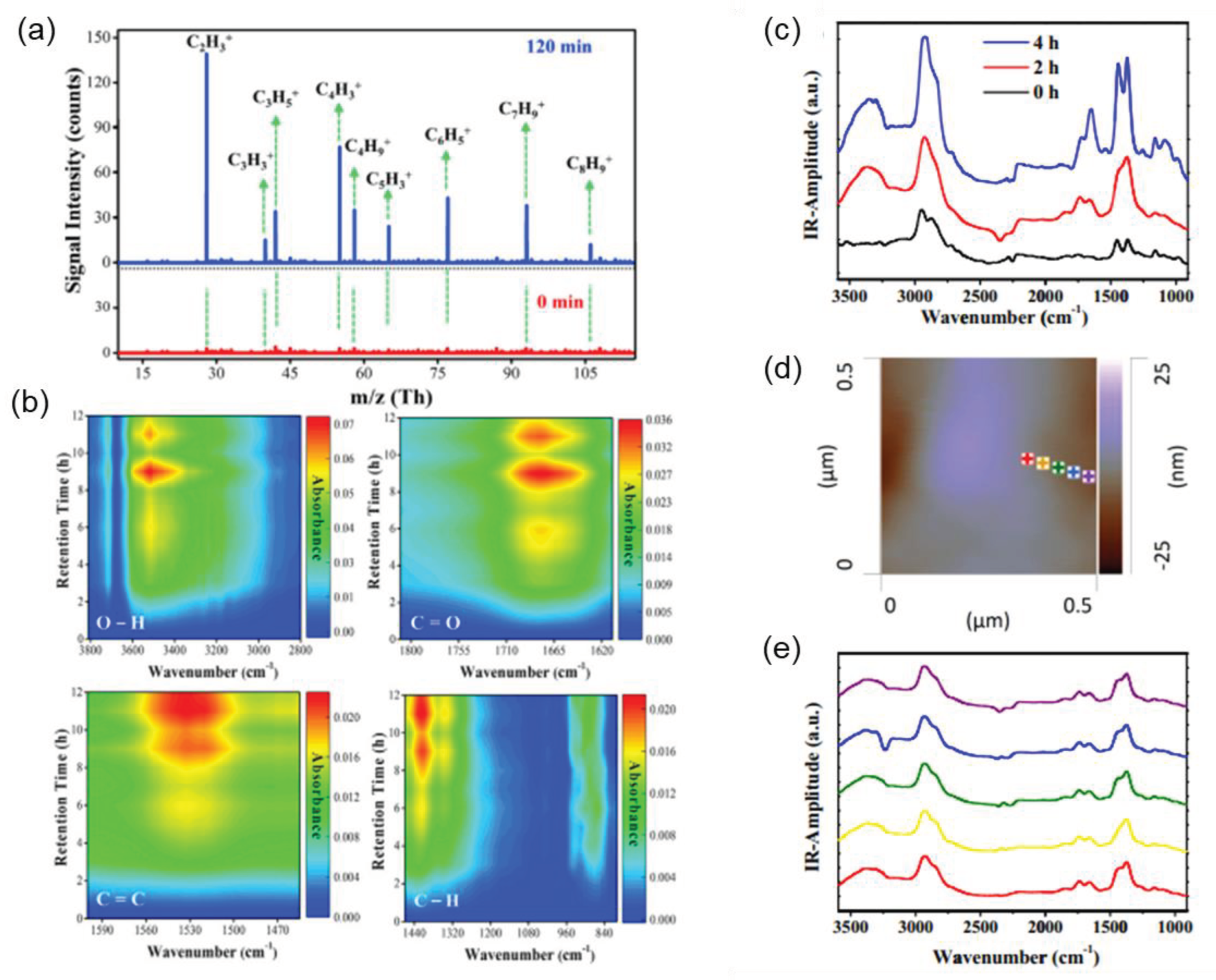
Numerous existing techniques can be employed for the characterization of photocatalytic MPs to examine surface morphological changes, the formation of functional groups, free radicals, and other by-products. For example, Cho et al. [93] investigated the photodegradation of the poly(vinyl chloride) (PVC) films with and without TiO2 using weight loss monitoring, scanning electron microscopic (SEM) analysis, gel permeation chromatography (GPC), FT-IR and UV–VIS spectroscopy, and X-ray photoelectron spectroscopy (XPS). Nabi et al. [89] used DRIFTS and high-pressure photon ionization (HPPI) (Figure 8a) coupled with time-of-flight mass spectrometry (TOFMS) (Figure 8b) to detect the functional groups generated during the photodegradation of polystyrene (PS), such as hydroxyl, carbonyl, and carbon-hydrogen groups. Moreover, Luo et al. [94] utilized an atomic force microscopy-infrared (AFM-IR) (Figure 8 c-d) instrument to investigate surface coatings of MPs. He and his colleagues also detected an increased signal intensity of vinylidene end groups and a gradual decrease in the average softening temperature of MPs through FTIR spectroscopy and localized thermal analysis (TA), as irradiation time increased. Furthermore, the mechanical properties of MPs were able to be analyzed by Lorentz Contact Resonance (LCR) measurements of a contact resonance AFM. Furthermore, 14C isotope tracer, spectroscopic, and chromatographic techniques were also used by Tian et al. [95] to investigate the photodegradation process of PS NPs in air and water. Researchers can utilize these advanced analytical methods to gain a deeper understanding of photocatalytic processes, shed light on underlying mechanisms, and optimize material properties.
3.2. Mechanism of Photocatalysis
Generally, there are two principal mechanisms that govern photocatalytic processes: free radical mechanism and singlet oxygen mechanism. The underlying pathways of these processes play an essential role in determining the efficacy of degradation and will be discussed in greater detail in the following sections.
3.2.1. Free Radical Mechanism
After absorbing light, the photocatalysts generate and separate photoelectrons in the conduction band and holes in the valence band. The generated photoelectrons and holes migrate to the surface of the photocatalyst and react with other chemical species. Specifically, a photoelectron that reaches the catalyst surface and encounters O2 molecules facilitates their reduction to O2•- radicals, which subsequently react with water molecules to produce unstable •OOH radicals. In the next step, the radicals may break down into hydrogen peroxide and oxygen molecules and, under further irradiation, hydrogen peroxide can further break down into radicals known as •OH radicals. The highly reactive •OH radicals are the key oxidizing agent in most of the advanced oxidation processes and are capable of degrading plastics [96,97,98].
Meanwhile, the holes (h+) located in the valence band can also migrate to the photocatalyst surface, where they oxidize plastics directly or react with H2O adsorbed to generate more •OH radicals, which in turn degrades the plastic into a variety of small molecular organic compounds, or CO2 and H2O[11].
A normalized decomposition process is suggested below. To be more specific, the weak spots (such as chromophoric groups or defects) of MPs will first be initiated by the generated reactive oxygen species (•OH) and alkyl radicals [18]. Then, the oxygen will be incorporated in oxygen molecules and thus can easily lead to chain cleavage, branching, and crosslinking.
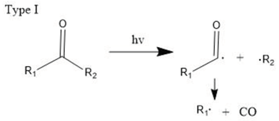
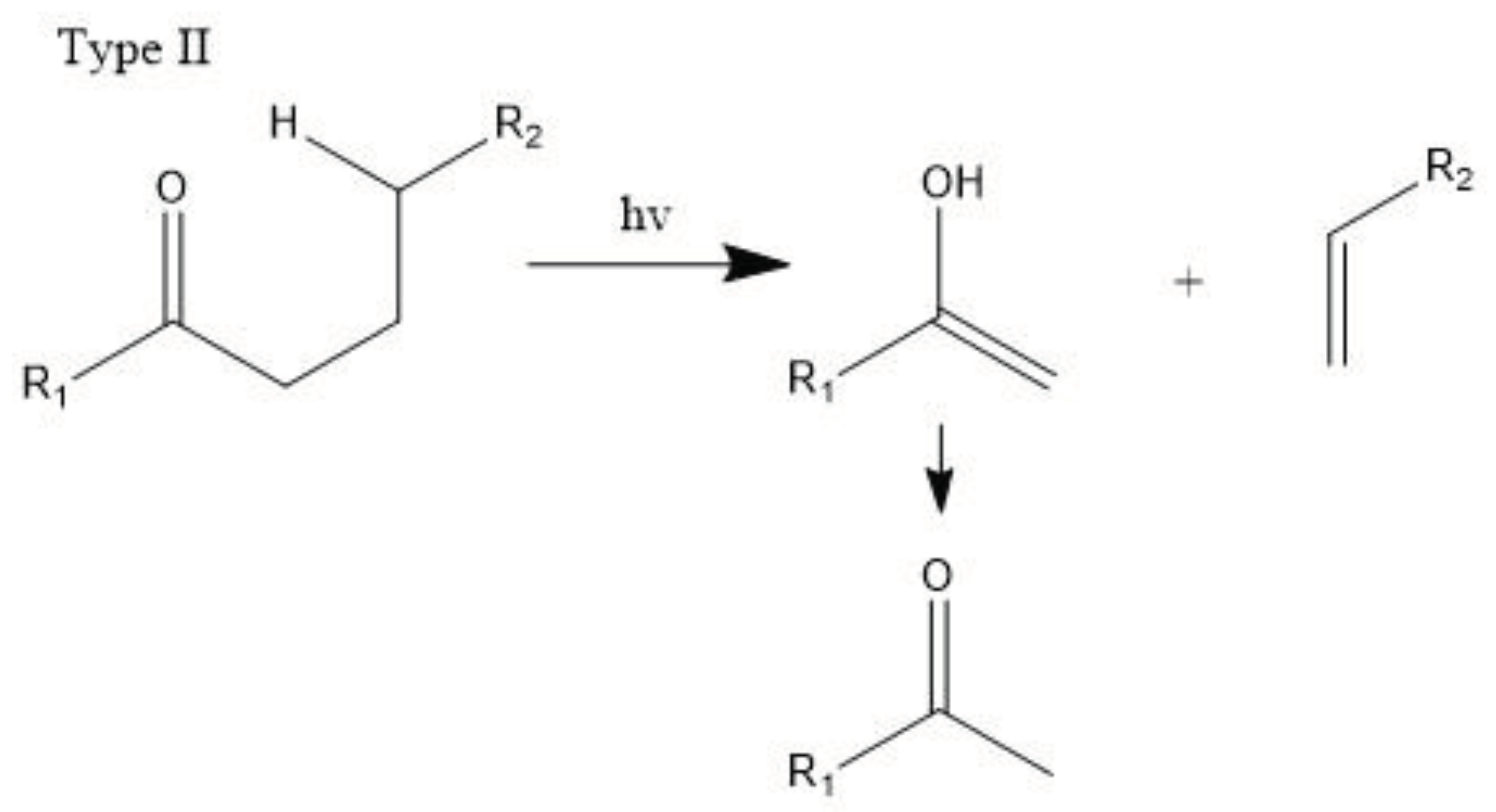
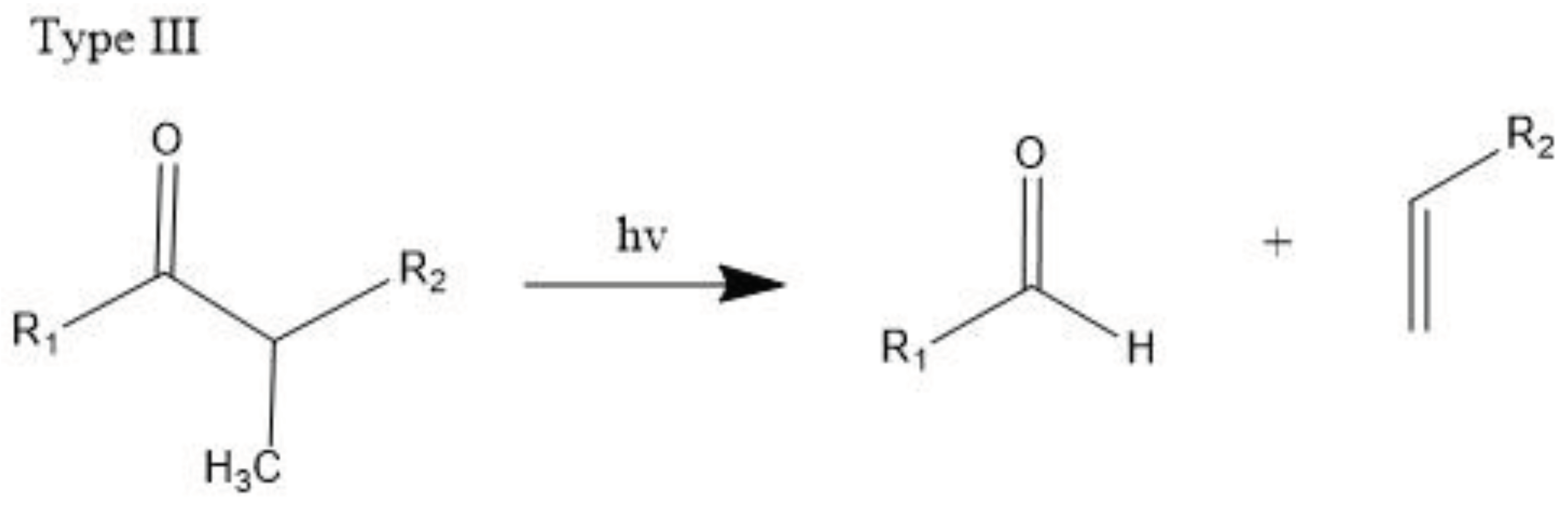
The carbonyl radicals generated can further decompose through the Norrish reactions, which are a series of photodegradation processes that involve the cleavage of polymer chains under irradiation [99]. The Norrish reactions were categorized based on their mechanistic pathways, radical or non-radical nature, and the types of chemical species produced as a result of the reactions. The Norrish type I reaction entails the cleavage of the bond between the carbonyl group and the α-carbon atom (α-scission), leading to the formation of carbon (II) oxide (CO). The Norrish type II reaction is a non-radical process that involves hydrogen atom abstraction from the γ-carbon atom, resulting in the decomposition of the polymer into an unsaturated chain and a chain with a carbonyl group end. Meanwhile, the Norrish type III reaction is another non-radical chain scission process that involves the transfer of a β-hydrogen atom, ultimately yielding an olefin and an aldehyde [18,99,100,101]. The likelihood of each Norrish reaction occurring varies depending on their respective activation energies, which dictate the ease of the reaction under specific conditions [99,101].
Then, polymers become more brittle, and the molecule’s weight decreases as a result of the effect of the entire process, which further facilitates degradation. Lastly, upon further oxidation, mineralization occurs to produce carbon dioxide and water as explained below.
3.2.2. Singlet Oxygen Oxidation Mechanism
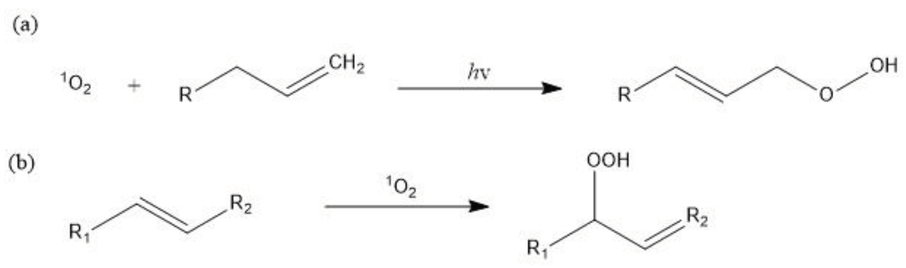
An alternative mechanism to photodegrade MPs is through oxidizing singlet oxygen, which can be generated through photochemical, thermal, chemical, and enzymatic reactions [102,103]. In this mechanism, singlet oxygen—a highly reactive form of molecular oxygen—directly reacts with and oxidize plastics, causing subsequent chain scission [104]. The generation of singlet oxygen relies on the presence of suitable sensitizers, which are molecules capable of absorbing light and transitioning to a triplet state [105]. This triplet state can then facilitate the conversion of triplet state oxygen into the highly reactive singlet state. By harnessing the reactive power of singlet oxygen, this mechanism provides a promising avenue for photodegradation of plastics through direct oxidation.
The singlet oxygen formed is also capable of reacting with the vinyl group produced by a Norrish reaction [102]. This interaction prompts further decomposition of the molecule, culminating in chain scission and the emergence of the hydroperoxides functional group (ROOH), as illustrated in Figure 9. The detection of singlet oxygen can be achieved by EPR measurements and the singlet oxygen is demonstrated to be able to promote selective styrene oxidation through Scavenger-assisted photocatalytic experiments according to Cheng et al. [106,107]
4. Conclusion and Perspectives
The increasing prevalence of microplastics in our ecosystems has given rise to significant environmental and health concerns. Photocatalysis, as an eco-friendly solution, has garnered considerable attention for its potential in addressing different environmental problems. Notably, while numerous factors can influence the degradation process, the overarching determinant lies in the potency of the photocatalysts themselves. Through various material enhancement strategies, such as doping and heterojunction construction, the efficiency of this degradation process can be amplified. Moreover, a deep understanding of the underlying mechanisms, including free radical mechanism and the singlet oxygen oxidation pathway, was introduced in this review and is essential for further optimization of the photodegradation efficiency.
However, the exploration of those advanced modification strategies photocatalytic nanomaterials in microplastic degradation remains limited, such as defect engineering and surface and morphology modification, signifying a potent area for groundbreaking progress in environmental remediation. Except from the photocatalysts modification, future directions of the photodegradation should address the sustainability of photocatalytic processes, emphasizing the long-term stability, reusability, and economic feasibility of these nanomaterials. It is also paramount to evaluate the environmental implications of degradation products and any potential toxicity associated with the photocatalysts themselves. Moreover, while the technological strides are commendable, the economic underpinnings of these strategies need careful consideration for broad-scale applications. In totality, the challenge posed by microplastics necessitates ongoing innovations, collaborations, and a holistic view of the environmental, technical, and economic facets of the solution.
Author Contributions
Conceptualization, Y.X. and Y.T.; methodology, Y.X. and Y.T.; software, Y.X. and Y.T.; validation, Y.X. and Y.T.; formal analysis, Y.X. and Y.T.; investigation, Y.T.; resources, J.Z.; data curation, Y.X.; writing—original draft preparation, Y.X. and Y.T.; writing—review and editing, Y.X., Y.T., W. X. and J.Z.; visualization, Y.X. and Y.T.; supervision, J.Z.; project administration, J.Z.; funding acquisition, J.Z. All authors have read and agreed to the published version of the manuscript.
Funding
This research was funded by Arkansas Agriculture Experiment Station of the University of Arkansas Division of Agriculture and the Center for Agricultural and Rural Sustainability (Hatch project: ARK02604).
Acknowledgements
This research was supported by the Arkansas Agriculture Experiment Station of the University of Arkansas Division of Agriculture and the Center for Agricultural and Rural Sustainability.
Conflicts of Interest
The authors declare no conflicts of interest.
References
- OECD iLibrary Plastics Use in 2019 Available online:. Available online: https://www.oecd-ilibrary.org/environment/data/global-plastic-outlook/plastics-use-in-2019_efff24eb-en (accessed on 13 February 2023).
- Häder, D.-P.; Banaszak, A.T.; Villafañe, V.E.; Narvarte, M.A.; González, R.A.; Helbling, E.W. Anthropogenic Pollution of Aquatic Ecosystems: Emerging Problems with Global Implications. Science of The Total Environment 2020, 713, 136586. [Google Scholar] [CrossRef]
- Erren, T.; Zeuß, D.; Steffany, F.; Meyer-Rochow, B. Increase of Wildlife Cancer: An Echo of Plastic Pollution? Nat Rev Cancer 2009, 9, 842–842. [Google Scholar] [CrossRef] [PubMed]
- Machovsky-Capuska, G.E.; Amiot, C.; Denuncio, P.; Grainger, R.; Raubenheimer, D. A Nutritional Perspective on Plastic Ingestion in Wildlife. Science of The Total Environment 2019, 656, 789–796. [Google Scholar] [CrossRef] [PubMed]
- Shen, M.; Huang, W.; Chen, M.; Song, B.; Zeng, G.; Zhang, Y. (Micro)Plastic Crisis: Un-Ignorable Contribution to Global Greenhouse Gas Emissions and Climate Change. Journal of Cleaner Production 2020, 254, 120138. [Google Scholar] [CrossRef]
- Elkhatib, D.; Oyanedel-Craver, V. A Critical Review of Extraction and Identification Methods of Microplastics in Wastewater and Drinking Water. Environ. Sci. Technol. 2020, 54, 7037–7049. [Google Scholar] [CrossRef] [PubMed]
- Wright, S.L.; Thompson, R.C.; Galloway, T.S. The Physical Impacts of Microplastics on Marine Organisms: A Review. Environmental Pollution 2013, 178, 483–492. [Google Scholar] [CrossRef]
- Hermabessiere, L.; Dehaut, A.; Paul-Pont, I.; Lacroix, C.; Jezequel, R.; Soudant, P.; Duflos, G. Occurrence and Effects of Plastic Additives on Marine Environments and Organisms: A Review. Chemosphere 2017, 182, 781–793. [Google Scholar] [CrossRef]
- Zazouli, M.; Nejati, H.; Hashempour, Y.; Dehbandi, R.; Nam, V.T.; Fakhri, Y. Occurrence of Microplastics (MPs) in the Gastrointestinal Tract of Fishes: A Global Systematic Review and Meta-Analysis and Meta-Regression. Science of The Total Environment 2022, 815, 152743. [Google Scholar] [CrossRef]
- Menéndez-Pedriza, A.; Jaumot, J. Interaction of Environmental Pollutants with Microplastics: A Critical Review of Sorption Factors, Bioaccumulation and Ecotoxicological Effects. Toxics 2020, 8, 40. [Google Scholar] [CrossRef]
- Chu, S.; Zhang, B.; Zhao, X.; Soo, H.S.; Wang, F.; Xiao, R.; Zhang, H. Photocatalytic Conversion of Plastic Waste: From Photodegradation to Photosynthesis. Advanced Energy Materials 2022, 12, 2200435. [Google Scholar] [CrossRef]
- Santos, R.G.; E. ; Capuska; HTTPS://ORCID.ORG/0000-0001-8698-8424; Andrades, R. Plastic Ingestion as an Evolutionary Trap: Toward a Holistic Understanding. Science 2021, 373, 56–60. [Google Scholar] [CrossRef] [PubMed]
- Leslie, H.A.; van Velzen, M.J.M.; Brandsma, S.H.; Vethaak, A.D.; Garcia-Vallejo, J.J.; Lamoree, M.H. Discovery and Quantification of Plastic Particle Pollution in Human Blood. Environ Int 2022, 163, 107199. [Google Scholar] [CrossRef] [PubMed]
- Microbead-Free Waters Act of 2015; 2015; p. Public Law No.114-114 Stat. 3129.
- International Union for Conservation of Nature IUCN 2017 : International Union for Conservation of Nature Annual Report 2017; IUCN, 2018.
- Lin, S.; Huang, H.; Ma, T.; Zhang, Y. Photocatalytic Oxygen Evolution from Water Splitting. Advanced Science 2021, 8, 2002458. [Google Scholar] [CrossRef] [PubMed]
- Ma, Y.; Wang, X.; Jia, Y.; Chen, X.; Han, H.; Li, C. Titanium Dioxide-Based Nanomaterials for Photocatalytic Fuel Generations. Chem. Rev. 2014, 114, 9987–10043. [Google Scholar] [CrossRef] [PubMed]
- Tofa, T.S.; Kunjali, K.L.; Paul, S.; Dutta, J. Visible Light Photocatalytic Degradation of Microplastic Residues with Zinc Oxide Nanorods. Environ Chem Lett 2019, 17, 1341–1346. [Google Scholar] [CrossRef]
- Kavitha, R.; Nithya, P.M.; Girish Kumar, S. Noble Metal Deposited Graphitic Carbon Nitride Based Heterojunction Photocatalysts. Applied Surface Science 2020, 508, 145142. [Google Scholar] [CrossRef]
- Devi, L.G.; Kavitha, R. A Review on Non Metal Ion Doped Titania for the Photocatalytic Degradation of Organic Pollutants under UV/Solar Light: Role of Photogenerated Charge Carrier Dynamics in Enhancing the Activity. Applied Catalysis B: Environmental 2013, 140–141, 559–587. [Google Scholar] [CrossRef]
- Du, S.; Lin, S.; Ren, K.; Li, C.; Zhang, F. Revealing the Effects of Transition Metal Doping on CoSe Cocatalyst for Enhancing Photocatalytic H2 Production. Applied Catalysis B: Environmental 2023, 328, 122503. [Google Scholar] [CrossRef]
- Rehman, S.; Ullah, R.; Butt, A.M.; Gohar, N.D. Strategies of Making TiO2 and ZnO Visible Light Active. Journal of Hazardous Materials 2009, 170, 560–569. [Google Scholar] [CrossRef]
- Bai, S.; Zhang, N.; Gao, C.; Xiong, Y. Defect Engineering in Photocatalytic Materials. Nano Energy 2018, 53, 296–336. [Google Scholar] [CrossRef]
- Djurišić, A.B.; Leung, Y.H.; Ng, A.M.C. Strategies for Improving the Efficiency of Semiconductor Metal Oxide Photocatalysis. Mater. Horiz. 2014, 1, 400–410. [Google Scholar] [CrossRef]
- Feng, N.; Lin, H.; Song, H.; Yang, L.; Tang, D.; Deng, F.; Ye, J. Efficient and Selective Photocatalytic CH4 Conversion to CH3OH with O2 by Controlling Overoxidation on TiO2. Nat Commun 2021, 12, 4652. [Google Scholar] [CrossRef]
- Peng, X.; Zhang, Y.; Liu, Y. Fabrication of a Novel High Photocatalytic Ag/Ag3PO4/P25 (TiO2) Heterojunction Catalyst for Reducing Electron-Hole Pair Recombination and Improving Photo-Corrosion. Mater. Res. Express 2019, 6, 065515. [Google Scholar] [CrossRef]
- Zhao, W.; Ma, W.; Chen, C.; Zhao, J.; Shuai, Z. Efficient Degradation of Toxic Organic Pollutants with Ni2O3/TiO2-XBx under Visible Irradiation. J. Am. Chem. Soc. 2004, 126, 4782–4783. [Google Scholar] [CrossRef] [PubMed]
- Inoue, T.; Fujishima, A.; Konishi, S.; Honda, K. Photoelectrocatalytic Reduction of Carbon Dioxide in Aqueous Suspensions of Semiconductor Powders. Nature 1979, 277, 637–638. [Google Scholar] [CrossRef]
- Habisreutinger, S.N.; Schmidt-Mende, L.; Stolarczyk, J.K. Photocatalytic Reduction of CO2 on TiO2 and Other Semiconductors. Angewandte Chemie International Edition 2013, 52, 7372–7408. [Google Scholar] [CrossRef] [PubMed]
- Wang, C.-C.; Li, J.-R.; Lv, X.-L.; Zhang, Y.-Q.; Guo, G. Photocatalytic Organic Pollutants Degradation in Metal–Organic Frameworks. Energy & Environmental Science 2014, 7, 2831–2867. [Google Scholar] [CrossRef]
- Xiao, Y.; Tian, Y.; Zhan, Y.; Zhu, J. DEGRADATION OF ORGANIC POLLUTANTS IN FLOCCULATED LIQUID DIGESTATE USING PHOTOCATALYTIC TITANATE NANOFIBERS: MECHANISM AND RESPONSE SURFACE OPTIMIZATION. Front. Agr. Sci. Eng. 2023, 0. [Google Scholar] [CrossRef]
- Ye, X.; Tian, Y.; Gao, M.; Cheng, F.; Lan, J.; Chen, H.; Lanoue, M.; Huang, S.; Tian, R. Efficient Photocatalytic Core/Shell of Titanate Nanowire/RGO 2024.
- Li, C.; Xu, Y.; Tu, W.; Chen, G.; Xu, R. Metal-Free Photocatalysts for Various Applications in Energy Conversion and Environmental Purification. Green Chemistry 2017, 19, 882–899. [Google Scholar] [CrossRef]
- Wang, L.; Zhao, J.; Liu, H.; Huang, J. Design, Modification and Application of Semiconductor Photocatalysts. Journal of the Taiwan Institute of Chemical Engineers 2018, 93, 590–602. [Google Scholar] [CrossRef]
- Shao, W.; Wang, H.; Zhang, X. Elemental Doping for Optimizing Photocatalysis in Semiconductors. Dalton Trans. 2018, 47, 12642–12646. [Google Scholar] [CrossRef]
- Tian, Y.; Zhang, L.; Xiao, Y.; Collins, T.; Akhter, A.; Huang, Y.; Tian, Z.R. Mo-Doped Titanate Nanofibers from Hydrothermal Syntheses for Improving Bone Scaffold. Characterization and Application of Nanomaterials 2024, 7, 3587. [Google Scholar] [CrossRef]
- Schöttner, L.; Erker, S.; Schlesinger, R.; Koch, N.; Nefedov, A.; Hofmann, O.T.; Wöll, C. Doping-Induced Electron Transfer at Organic/Oxide Interfaces: Direct Evidence from Infrared Spectroscopy. J. Phys. Chem. C 2020, 124, 4511–4516. [Google Scholar] [CrossRef] [PubMed]
- Khaki, M.R.D.; Shafeeyan, M.S.; Raman, A.A.A.; Daud, W.M.A.W. Application of Doped Photocatalysts for Organic Pollutant Degradation - A Review. Journal of Environmental Management 2017, 198, 78–94. [Google Scholar] [CrossRef] [PubMed]
- Matsuo, H.; Noguchi, Y.; Miyayama, M. Gap-State Engineering of Visible-Light-Active Ferroelectrics for Photovoltaic Applications. Nat Commun 2017, 8, 207. [Google Scholar] [CrossRef] [PubMed]
- Cole, P.; Tian, Y.; Thornburgh, S.; Malloy, M.; Roeder, L.; Zhang, L.; Patel, M.; Xiao, Y.; Huang, Y.; Tian, Z.R. Hydrothermal Synthesis of Valve Metal Ta-Doped Titanate Nanofibers for Potentially Engineering Bone Tissue. Characterization and Application of Nanomaterials 2024, 6, 3606. [Google Scholar] [CrossRef]
- Tripathi, A.K.; Mathpal, M.C.; Kumar, P.; Singh, M.K.; Soler, M.A.G.; Agarwal, A. Structural, Optical and Photoconductivity of Sn and Mn Doped TiO2 Nanoparticles. Journal of Alloys and Compounds 2015, 622, 37–47. [Google Scholar] [CrossRef]
- Yao, B.; Peng, C.; Zhang, W.; Zhang, Q.; Niu, J.; Zhao, J. A Novel Fe(III) Porphyrin-Conjugated TiO2 Visible-Light Photocatalyst. Applied Catalysis B: Environmental 2015, 174–175, 77–84. [Google Scholar] [CrossRef]
- Viswanathan, B.; Krishanmurthy, K.R. Nitrogen Incorporation in TiO2: Does It Make a Visible Light Photo-Active Material? International Journal of Photoenergy 2012, 2012, e269654. [Google Scholar] [CrossRef]
- Hwang, Y.J.; Yang, S.; Lee, H. Surface Analysis of N-Doped TiO2 Nanorods and Their Enhanced Photocatalytic Oxidation Activity. Applied Catalysis B: Environmental 2017, 204, 209–215. [Google Scholar] [CrossRef]
- Kang, J.; Zhou, L.; Duan, X.; Sun, H.; Ao, Z.; Wang, S. Degradation of Cosmetic Microplastics via Functionalized Carbon Nanosprings. Matter 2019, 1, 745–758. [Google Scholar] [CrossRef]
- Zhou, D.; Luo, H.; Zhang, F.; Wu, J.; Yang, J.; Wang, H. Efficient Photocatalytic Degradation of the Persistent PET Fiber-Based Microplastics over Pt Nanoparticles Decorated N-Doped TiO2 Nanoflowers. Adv. Fiber Mater. 2022, 4, 1094–1107. [Google Scholar] [CrossRef]
- Low, J.; Yu, J.; Jaroniec, M.; Wageh, S.; Al-Ghamdi, A.A. Heterojunction Photocatalysts. Advanced Materials 2017, 29, 1601694. [Google Scholar] [CrossRef] [PubMed]
- Qin, J.; Dou, Y.; Wu, F.; Yao, Y.; Andersen, H.R.; Hélix-Nielsen, C.; Lim, S.Y.; Zhang, W. In-Situ Formation of Ag2O in Metal-Organic Framework for Light-Driven Upcycling of Microplastics Coupled with Hydrogen Production. Applied Catalysis B: Environmental 2022, 319, 121940. [Google Scholar] [CrossRef]
- Feng, B.; Wu, Z.; Liu, J.; Zhu, K.; Li, Z.; Jin, X.; Hou, Y.; Xi, Q.; Cong, M.; Liu, P.; et al. Combination of Ultrafast Dye-Sensitized-Assisted Electron Transfer Process and Novel Z-Scheme System: AgBr Nanoparticles Interspersed MoO3 Nanobelts for Enhancing Photocatalytic Performance of RhB. Applied Catalysis B: Environmental 2017, 206, 242–251. [Google Scholar] [CrossRef]
- Bard, A.J. Photoelectrochemistry and Heterogeneous Photo-Catalysis at Semiconductors. Journal of Photochemistry 1979, 10, 59–75. [Google Scholar] [CrossRef]
- Zhou, D.; Wang, L.; Zhang, F.; Wu, J.; Wang, H.; Yang, J. Feasible Degradation of Polyethylene Terephthalate Fiber-Based Microplastics in Alkaline Media with Bi2O3@N-TiO2 Z-Scheme Photocatalytic System. Advanced Sustainable Systems 2022, 6, 2100516. [Google Scholar] [CrossRef]
- Xu, Q.; Zhang, L.; Yu, J.; Wageh, S.; Al-Ghamdi, A.A.; Jaroniec, M. Direct Z-Scheme Photocatalysts: Principles, Synthesis, and Applications. Materials Today 2018, 21, 1042–1063. [Google Scholar] [CrossRef]
- Zhang, W.; Mohamed, A.R.; Ong, W.-J. Z-Scheme Photocatalytic Systems for Carbon Dioxide Reduction: Where Are We Now? Angewandte Chemie International Edition 2020, 59, 22894–22915. [Google Scholar] [CrossRef] [PubMed]
- Liang, Z.; Wen, Q.; Wang, X.; Zhang, F.; Yu, Y. Chemically Stable and Reusable Nano Zero-Valent Iron/Graphite-like Carbon Nitride Nanohybrid for Efficient Photocatalytic Treatment of Cr(VI) and Rhodamine B under Visible Light. Applied Surface Science 2016, 386, 451–459. [Google Scholar] [CrossRef]
- Fu, J.; Xu, Q.; Low, J.; Jiang, C.; Yu, J. Ultrathin 2D/2D WO3/g-C3N4 Step-Scheme H2-Production Photocatalyst. Applied Catalysis B: Environmental 2019, 243, 556–565. [Google Scholar] [CrossRef]
- Yang, M.; Li, Y.; Jin, Z. In Situ XPS Proved Graphdiyne (CnH2n-2)-Based CoFe LDH/CuI/GD Double S-Scheme Heterojunction Photocatalyst for Hydrogen Evolution. Separation and Purification Technology 2023, 311, 123229. [Google Scholar] [CrossRef]
- Li, Z.; Ai, W.; Zhang, Y.; Zhang, J.; Liu, W.; Zhong, D.; Cai, Y.; Johansson, E.; Boschloo, G.; Jin, W.; et al. Magnetic Carbon Nanotube Modified S-Scheme TiO2-x/g-C3N4/CNFe Heterojunction Coupled with Peroxymonosulfate for Effective Visible-Light-Driven Photodegradation via Enhanced Interfacial Charge Separation. Separation and Purification Technology 2023, 308, 122897. [Google Scholar] [CrossRef]
- Xu, Q.; Zhang, L.; Cheng, B.; Fan, J.; Yu, J. S-Scheme Heterojunction Photocatalyst. Chem 2020, 6, 1543–1559. [Google Scholar] [CrossRef]
- Michelin, C.; Hoffmann, N. Photosensitization and Photocatalysis—Perspectives in Organic Synthesis. ACS Catal. 2018, 8, 12046–12055. [Google Scholar] [CrossRef]
- Narayan, M.R. Review: Dye Sensitized Solar Cells Based on Natural Photosensitizers. Renewable and Sustainable Energy Reviews 2012, 16, 208–215. [Google Scholar] [CrossRef]
- Zhao, X.; Li, Z.; Chen, Y.; Shi, L.; Zhu, Y. Enhancement of Photocatalytic Degradation of Polyethylene Plastic with CuPc Modified TiO2 Photocatalyst under Solar Light Irradiation. Applied Surface Science 2008, 254, 1825–1829. [Google Scholar] [CrossRef]
- Hou, S.; Gao, X.; Lv, X.; Zhao, Y.; Yin, X.; Liu, Y.; Fang, J.; Yu, X.; Ma, X.; Ma, T.; et al. Decade Milestone Advancement of Defect-Engineered g-C3N4 for Solar Catalytic Applications. Nano-Micro Lett. 2024, 16, 70. [Google Scholar] [CrossRef] [PubMed]
- Wang, Q.; Lei, Y.; Wang, D.; Li, Y. Defect Engineering in Earth-Abundant Electrocatalysts for CO 2 and N 2 Reduction. Energy & Environmental Science 2019, 12, 1730–1750. [Google Scholar] [CrossRef]
- Zhang, S.; Si, Y.; Li, B.; Yang, L.; Dai, W.; Luo, S. Atomic-Level and Modulated Interfaces of Photocatalyst Heterostructure Constructed by External Defect-Induced Strategy: A Critical Review. Small 2021, 17, 2004980. [Google Scholar] [CrossRef]
- Ai, M.; Zhang, J.-W.; Wu, Y.-W.; Pan, L.; Shi, C.; Zou, J.-J. Role of Vacancies in Photocatalysis: A Review of Recent Progress. Chemistry – An Asian Journal 2020, 15, 3599–3619. [Google Scholar] [CrossRef]
- Liu, D.; Ni, K.; Ye, J.; Xie, J.; Zhu, Y.; Song, L. Tailoring the Structure of Carbon Nanomaterials toward High-End Energy Applications. Advanced Materials 2018, 30, 1802104. [Google Scholar] [CrossRef]
- Jia, Y.; Zhang, L.; Du, A.; Gao, G.; Chen, J.; Yan, X.; Brown, C.L.; Yao, X. Defect Graphene as a Trifunctional Catalyst for Electrochemical Reactions. Advanced Materials 2016, 28, 9532–9538. [Google Scholar] [CrossRef] [PubMed]
- Wei, D.; Liu, Y.; Wang, Y.; Zhang, H.; Huang, L.; Yu, G. Synthesis of N-Doped Graphene by Chemical Vapor Deposition and Its Electrical Properties. Nano Lett. 2009, 9, 1752–1758. [Google Scholar] [CrossRef] [PubMed]
- Zhu, Y.P.; Guo, C.; Zheng, Y.; Qiao, S.-Z. Surface and Interface Engineering of Noble-Metal-Free Electrocatalysts for Efficient Energy Conversion Processes. Acc. Chem. Res. 2017, 50, 915–923. [Google Scholar] [CrossRef] [PubMed]
- Liu, B.; Wang, Y.; Peng, H.-Q.; Yang, R.; Jiang, Z.; Zhou, X.; Lee, C.-S.; Zhao, H.; Zhang, W. Iron Vacancies Induced Bifunctionality in Ultrathin Feroxyhyte Nanosheets for Overall Water Splitting. Advanced Materials 2018, 30, 1803144. [Google Scholar] [CrossRef]
- Li, H.; Tsai, C.; Koh, A.L.; Cai, L.; Contryman, A.W.; Fragapane, A.H.; Zhao, J.; Han, H.S.; Manoharan, H.C.; Abild-Pedersen, F.; et al. Activating and Optimizing MoS2 Basal Planes for Hydrogen Evolution through the Formation of Strained Sulphur Vacancies. Nature Mater 2016, 15, 48–53. [Google Scholar] [CrossRef]
- Wang, G.; Lv, S.; Shen, Y.; Li, W.; Lin, L.; Li, Z. Advancements in Heterojunction, Cocatalyst, Defect and Morphology Engineering of Semiconductor Oxide Photocatalysts. Journal of Materiomics 2024, 10, 315–338. [Google Scholar] [CrossRef]
- Batzill, M. Fundamental Aspects of Surface Engineering of Transition Metal Oxide Photocatalysts. Energy & Environmental Science 2011, 4, 3275–3286. [Google Scholar] [CrossRef]
- Jiang, R.; Lu, G.; Yan, Z.; Liu, J.; Wu, D.; Wang, Y. Microplastic Degradation by Hydroxy-Rich Bismuth Oxychloride. Journal of Hazardous Materials 2021, 405, 124247. [Google Scholar] [CrossRef]
- Yang, X.; Wang, D. Photocatalysis: From Fundamental Principles to Materials and Applications. ACS Appl. Energy Mater. 2018, 1, 6657–6693. [Google Scholar] [CrossRef]
- Knight, M.W.; Sobhani, H.; Nordlander, P.; Halas, N.J. Photodetection with Active Optical Antennas. Science 2011, 332, 702–704. [Google Scholar] [CrossRef] [PubMed]
- Zhang, X.; Chen, Y.L.; Liu, R.-S.; Tsai, D.P. Plasmonic Photocatalysis. Rep. Prog. Phys. 2013, 76, 046401. [Google Scholar] [CrossRef] [PubMed]
- Maulana, D.A.; Ibadurrohman, M. ; Slamet Synthesis of Nano-Composite Ag/TiO2 for Polyethylene Microplastic Degradation Applications. IOP Conf. Ser.: Mater. Sci. Eng. 2021, 1011, 012054. [Google Scholar] [CrossRef]
- Fadli, M.H.; Ibadurrohman, M.; Slamet, S. Microplastic Pollutant Degradation in Water Using Modified TiO2 Photocatalyst Under UV-Irradiation. IOP Conf. Ser.: Mater. Sci. Eng. 2021, 1011, 012055. [Google Scholar] [CrossRef]
- C. Warren, S.; Thimsen, E. Plasmonic Solar Water Splitting. Energy & Environmental Science 2012, 5, 5133–5146. [Google Scholar] [CrossRef]
- Linic, S.; Christopher, P.; Ingram, D.B. Plasmonic-Metal Nanostructures for Efficient Conversion of Solar to Chemical Energy. Nature Mater 2011, 10, 911–921. [Google Scholar] [CrossRef]
- Zhang, Y.; He, S.; Guo, W.; Hu, Y.; Huang, J.; Mulcahy, J.R.; Wei, W.D. Surface-Plasmon-Driven Hot Electron Photochemistry. Chem. Rev. 2018, 118, 2927–2954. [Google Scholar] [CrossRef]
- Xiao, M.; Jiang, R.; Wang, F.; Fang, C.; Wang, J.; Yu, J.C. Plasmon-Enhanced Chemical Reactions. J. Mater. Chem. A 2013, 1, 5790–5805. [Google Scholar] [CrossRef]
- Gordon, T.R.; Paik, T.; Klein, D.R.; Naik, G.V.; Caglayan, H.; Boltasseva, A.; Murray, C.B. Shape-Dependent Plasmonic Response and Directed Self-Assembly in a New Semiconductor Building Block, Indium-Doped Cadmium Oxide (ICO). Nano Lett. 2013, 13, 2857–2863. [Google Scholar] [CrossRef]
- Agrawal, A.; Kriegel, I.; Milliron, D.J. Shape-Dependent Field Enhancement and Plasmon Resonance of Oxide Nanocrystals. J. Phys. Chem. C 2015, 119, 6227–6238. [Google Scholar] [CrossRef]
- Manchala, S.; Elayappan, V.; Lee, H.-G.; Shanker, V. Chapter 7 - Plasmonic Photocatalysis: An Extraordinary Way to Harvest Visible Light. In Photocatalytic Systems by Design; Sakar, M., Balakrishna, R.G., Do, T.-O., Eds.; Elsevier, 2021; pp. 187–216 ISBN 978-0-12-820532-7.
- M’Bra, I.C.; García-Muñoz, P.; Drogui, P.; Keller, N.; Trokourey, A.; Robert, D. Heterogeneous Photodegradation of Pyrimethanil and Its Commercial Formulation with TiO2 Immobilized on SiC Foams. Journal of Photochemistry and Photobiology A: Chemistry 2019, 368, 1–6. [Google Scholar] [CrossRef]
- Allé, P.H.; Garcia-Muñoz, P.; Adouby, K.; Keller, N.; Robert, D. Efficient Photocatalytic Mineralization of Polymethylmethacrylate and Polystyrene Nanoplastics by TiO2/β-SiC Alveolar Foams. Environ Chem Lett 2021, 19, 1803–1808. [Google Scholar] [CrossRef]
- Nabi, I.; Bacha, A.-U.-R.; Li, K.; Cheng, H.; Wang, T.; Liu, Y.; Ajmal, S.; Yang, Y.; Feng, Y.; Zhang, L. Complete Photocatalytic Mineralization of Microplastic on TiO2 Nanoparticle Film. iScience 2020, 23, null. [Google Scholar] [CrossRef]
- Meng, X.; Peng, X.; Xue, J.; Wei, Y.; Sun, Y.; Dai, Y. A Biomass-Derived, All-Day-Round Solar Evaporation Platform for Harvesting Clean Water from Microplastic Pollution. J. Mater. Chem. A 2021, 9, 11013–11024. [Google Scholar] [CrossRef]
- Ricardo, I.A.; Alberto, E.A.; Silva Júnior, A.H.; Macuvele, D.L.P.; Padoin, N.; Soares, C.; Gracher Riella, H.; Starling, M.C.V.M.; Trovó, A.G. A Critical Review on Microplastics, Interaction with Organic and Inorganic Pollutants, Impacts and Effectiveness of Advanced Oxidation Processes Applied for Their Removal from Aqueous Matrices. Chemical Engineering Journal 2021, 424, 130282. [Google Scholar] [CrossRef]
- Luo, J.; Zhang, W.; Yang, H.; Fan, Q.; Xiong, F.; Liu, S.; Li, D.-S.; Liu, B. Halide Perovskite Composites for Photocatalysis: A Mini Review. EcoMat 2021, 3, e12079. [Google Scholar] [CrossRef]
- Cho, S.; Choi, W. Solid-Phase Photocatalytic Degradation of PVC–TiO2 Polymer Composites. Journal of Photochemistry and Photobiology A: Chemistry 2001, 143, 221–228. [Google Scholar] [CrossRef]
- Luo, H.; Xiang, Y.; Li, Y.; Zhao, Y.; Pan, X. Photocatalytic Aging Process of Nano-TiO2 Coated Polypropylene Microplastics: Combining Atomic Force Microscopy and Infrared Spectroscopy (AFM-IR) for Nanoscale Chemical Characterization. Journal of Hazardous Materials 2021, 404, 124159. [Google Scholar] [CrossRef]
- Tian, L.; Chen, Q.; Jiang, W.; Wang, L.; Xie, H.; Kalogerakis, N.; Ma, Y.; Ji, R. A Carbon-14 Radiotracer-Based Study on the Phototransformation of Polystyrene Nanoplastics in Water versus in Air. Environmental Science: Nano 2019, 6, 2907–2917. [Google Scholar] [CrossRef]
- Shang, J.; Chai, M.; Zhu, Y. Solid-Phase Photocatalytic Degradation of Polystyrene Plastic with TiO2 as Photocatalyst. Journal of Solid State Chemistry 2003, 174, 104–110. [Google Scholar] [CrossRef]
- Shang, J.; Chai, M.; Zhu, Y. Photocatalytic Degradation of Polystyrene Plastic under Fluorescent Light. Environ. Sci. Technol. 2003, 37, 4494–4499. [Google Scholar] [CrossRef]
- Shi, Y.; Liu, P.; Wu, X.; Shi, H.; Huang, H.; Wang, H.; Gao, S. Insight into Chain Scission and Release Profiles from Photodegradation of Polycarbonate Microplastics. Water Research 2021, 195, 116980. [Google Scholar] [CrossRef]
- Olajire, A.A.; Mohammed, A.A. Green Synthesis of Palladium Nanoparticles Using Ananas Comosus Leaf Extract for Solid-Phase Photocatalytic Degradation of Low Density Polyethylene Film. Journal of Environmental Chemical Engineering 2019, 7, 103270. [Google Scholar] [CrossRef]
- Venkataramana, C.; Botsa, S.M.; Shyamala, P.; Muralikrishna, R. Photocatalytic Degradation of Polyethylene Plastics by NiAl2O4 Spinels-Synthesis and Characterization. Chemosphere 2021, 265, 129021. [Google Scholar] [CrossRef]
- Roy, P.K.; Surekha, P.; Rajagopal, C.; Chatterjee, S.N.; Choudhary, V. Studies on the Photo-Oxidative Degradation of LDPE Films in the Presence of Oxidised Polyethylene. Polymer Degradation and Stability 2007, 92, 1151–1160. [Google Scholar] [CrossRef]
- Lee, Q.Y.; Li, H. Photocatalytic Degradation of Plastic Waste: A Mini Review. Micromachines (Basel) 2021, 12, 907. [Google Scholar] [CrossRef]
- Hrycay, E.G.; Bandiera, S.M. Chapter Two - Involvement of Cytochrome P450 in Reactive Oxygen Species Formation and Cancer. In Advances in Pharmacology; Hardwick, J.P., Ed.; Cytochrome P450 Function and Pharmacological Roles in Inflammation and Cancer; Academic Press, 2015; Vol. 74, pp. 35–84.
- Rabek, J.F.; Rånby, B. The Role of Singlet Oxygen in the Photooxidation of Polymers. Photochemistry and Photobiology 1978, 28, 557–569. [Google Scholar] [CrossRef]
- Schmidt, R. Photosensitized Generation of Singlet Oxygen. Photochemistry and Photobiology 2006, 82, 1161–1177. [Google Scholar] [CrossRef]
- Cheng, C.; Zhu, B.; Cheng, B.; Macyk, W.; Wang, L.; Yu, J. Catalytic Conversion of Styrene to Benzaldehyde over S-Scheme Photocatalysts by Singlet Oxygen. ACS Catal. 2023, 13, 459–468. [Google Scholar] [CrossRef]
- Yousif, E.; Haddad, R. Photodegradation and Photostabilization of Polymers, Especially Polystyrene: Review. Springerplus 2013, 2, 398. [Google Scholar] [CrossRef] [PubMed]
- Singh, B.; Sharma, N. Mechanistic Implications of Plastic Degradation. Polymer Degradation and Stability 2008, 93, 561–584. [Google Scholar] [CrossRef]
Figure 1.
(a) Wave functions and schematic electronic structures of transition metal (TM=Cr, Mn, Co, Ni and Cu)-doped BFO obtained from DFT calculations. Crystal and electronic structures of Mn-doped BFO. (b) Optimized crystal structure of Mn-doped BFO [Bi16(Fe15Mn)O48] in rhombohedral R3 symmetry, (c) total density of states (DOS) and partial DOS (PDOS) of Mn-3d, Fe-3d and O-2p and (d) electronic band structure. [39] Copyright © 2017 Springer Nature Limited.
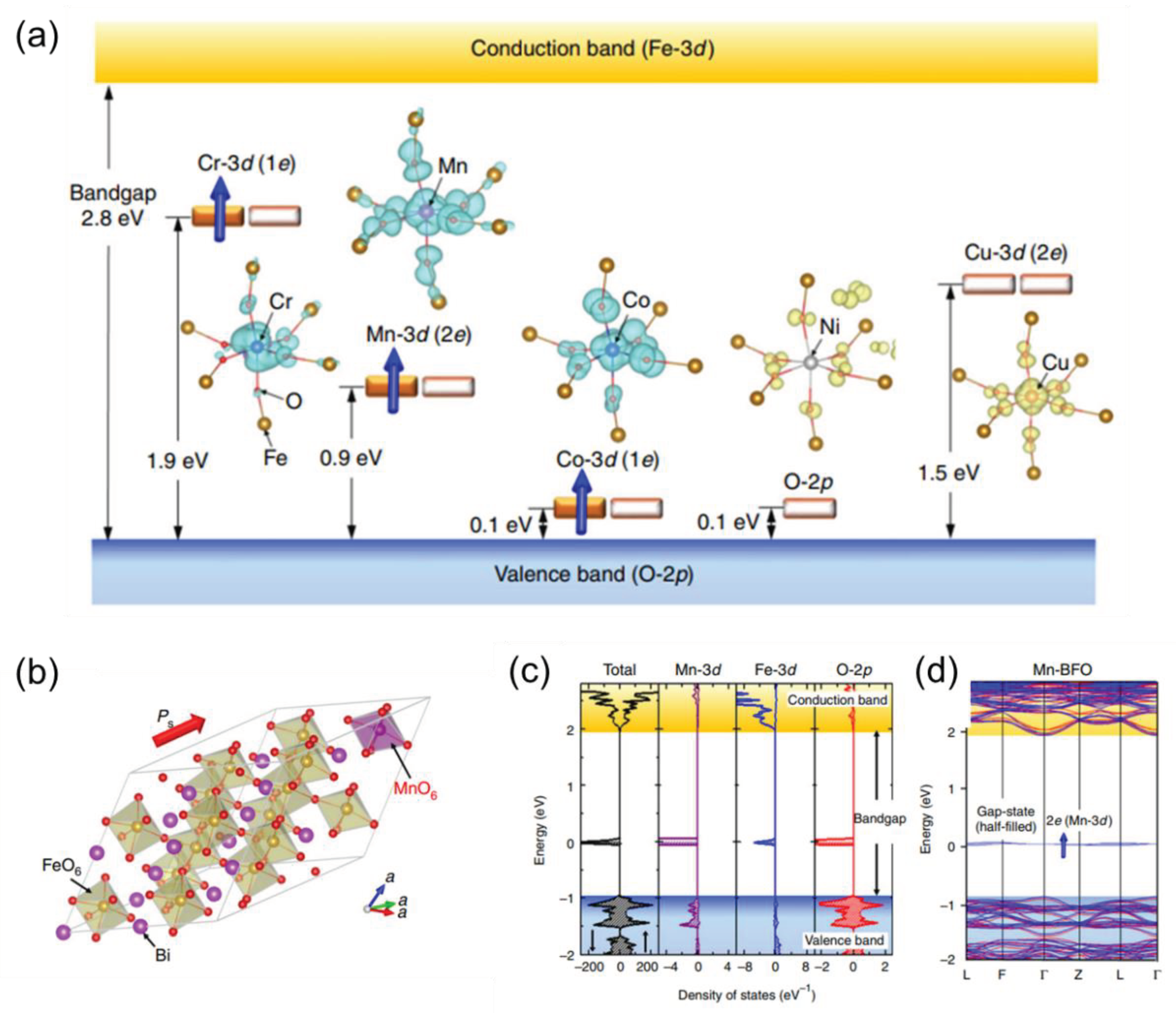
Figure 2.
(a,b) Valence spectra and (c,d) band gap measurements of (a,c) NTR-60 and (b,d) NTR-150. (Red dashed lines correspond to non-doped TR-60 and TR-150) [44] © 2016 Elsevier B.V. All rights reserved.
Figure 2.
(a,b) Valence spectra and (c,d) band gap measurements of (a,c) NTR-60 and (b,d) NTR-150. (Red dashed lines correspond to non-doped TR-60 and TR-150) [44] © 2016 Elsevier B.V. All rights reserved.
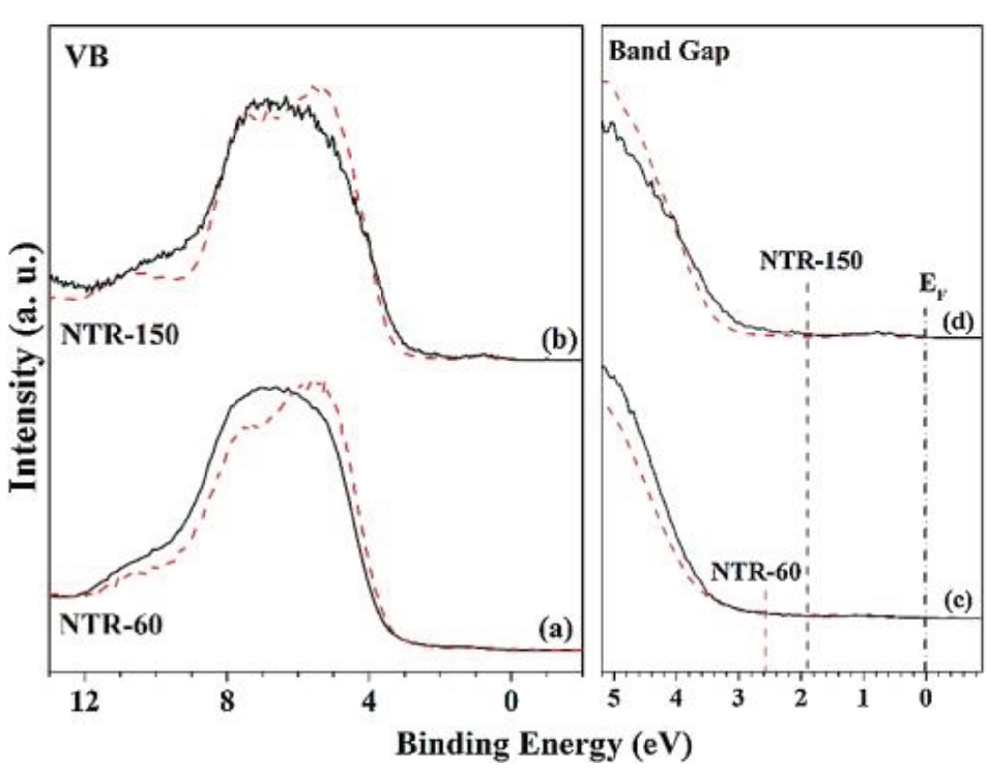
Figure 3.
Schematic illustration of the three different types of separation of electron–hole pairs in the case of conventional light-responsive heterojunction photocatalysts: a) type-I, b) type-II, and c) type-III heterojunctions. [47] © 2017 WILEY-VCH Verlag GmbH & Co. KGaA, Weinheim.
Figure 3.
Schematic illustration of the three different types of separation of electron–hole pairs in the case of conventional light-responsive heterojunction photocatalysts: a) type-I, b) type-II, and c) type-III heterojunctions. [47] © 2017 WILEY-VCH Verlag GmbH & Co. KGaA, Weinheim.
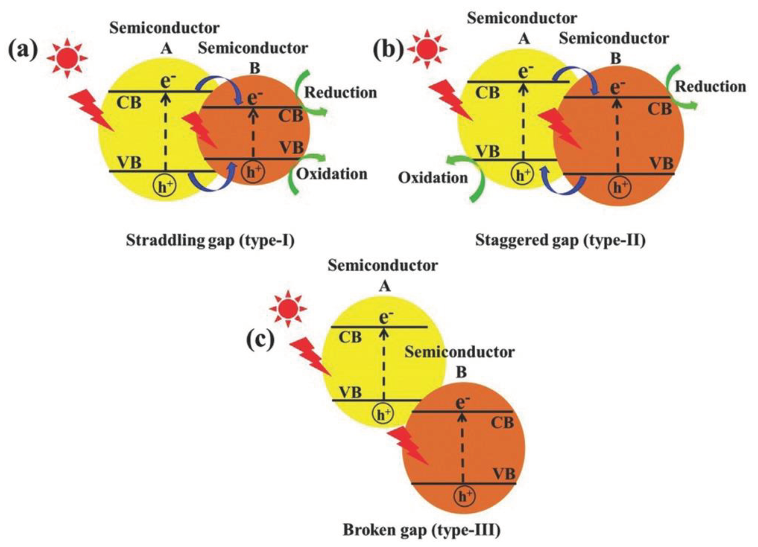
Figure 4.
a) Schematic diagram of the preparation process of the Bi2O3@N-TiO2. b) X-ray diffractometer (XRD) patterns of N-TiO2 and Bi2O3@N-TiO2-25%. c) Scanning electron microscope (SEM) image, d) transmission electron microscopy (TEM) image, e) HRTEM image and f) EDS elemental mappings of Bi2O3@N-TiO2-25%. Internal picture of (e) is the enlarged image of lattice spacing of N-TiO2 and Bi2O3. [51] © 2022 Wiley-VCH GmbH.
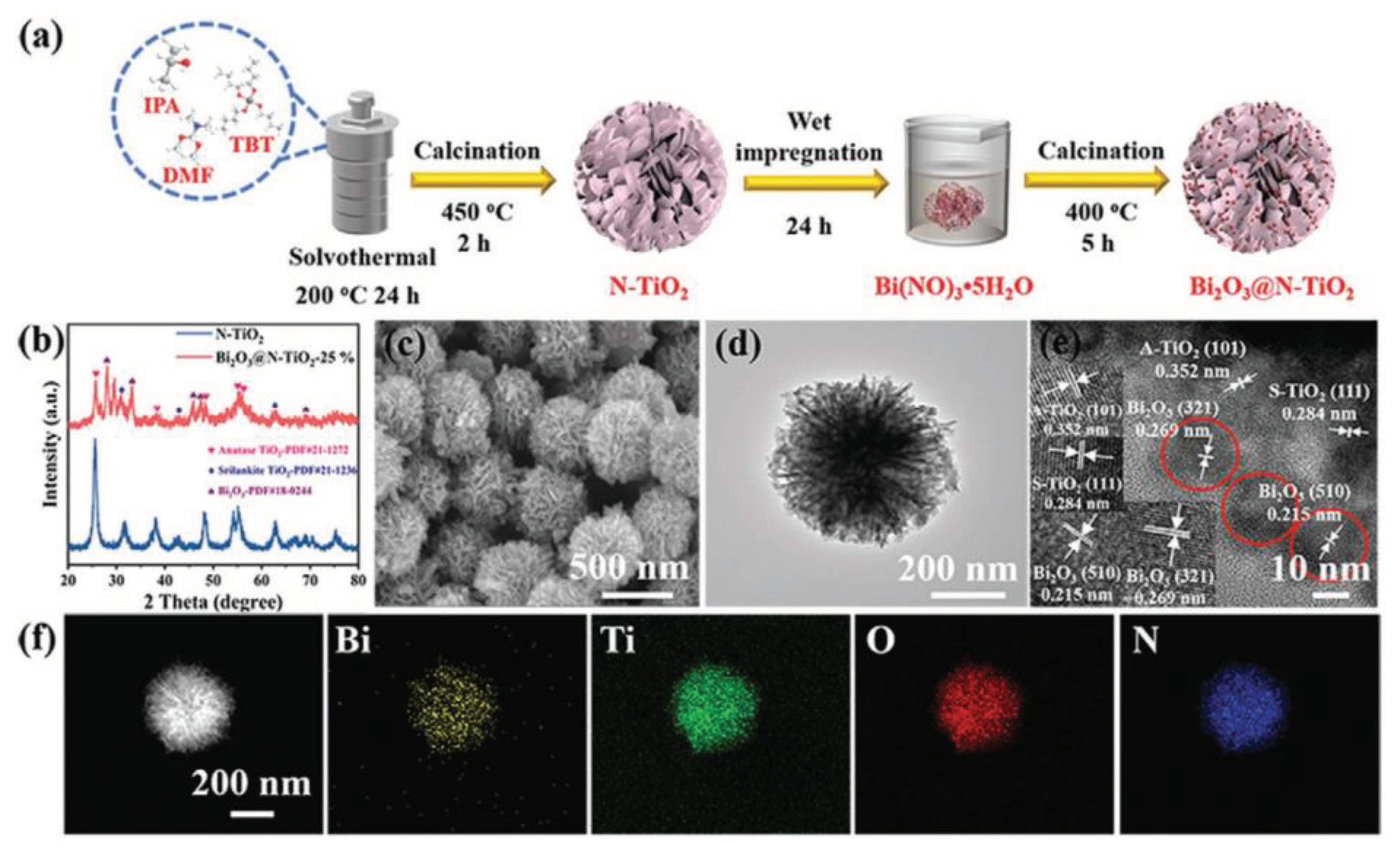
Figure 5.
Charge-Transfer Processes in an S-Scheme Heterojunction (A–C) Schematic illustration of heterojunction with staggered band configuration: (A) before contact, (B) after contact, (C) photogenerated charge carrier transfer process in S-scheme mode. [58] © 2020 Elsevier Inc.
Figure 5.
Charge-Transfer Processes in an S-Scheme Heterojunction (A–C) Schematic illustration of heterojunction with staggered band configuration: (A) before contact, (B) after contact, (C) photogenerated charge carrier transfer process in S-scheme mode. [58] © 2020 Elsevier Inc.
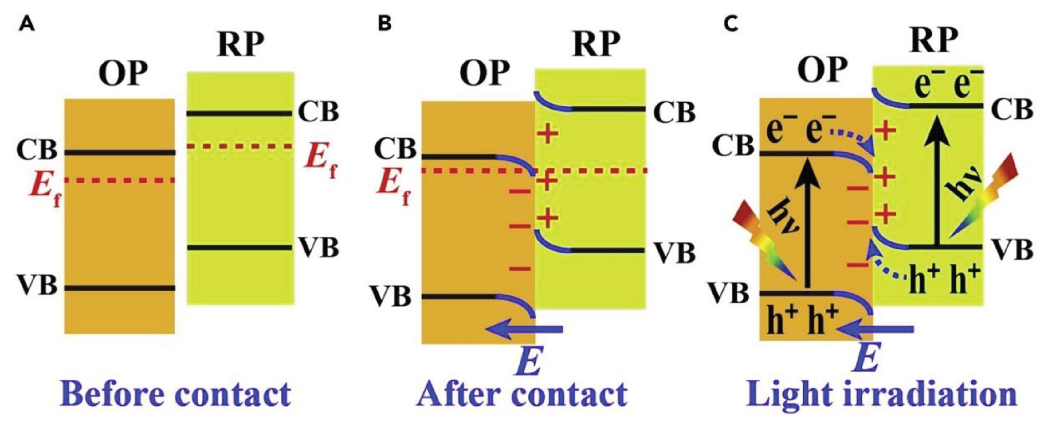
Figure 6.
(a) Schematic illustration of point defects and edges in graphene materials. Red atoms denote edges, green atoms denote vacancies, and blue atoms denote topological defects. Reprinted with permission from [66] Copyright 2018, John Wiley and Sons. (b) HAADF image of graphene possessing defects. Reprinted with permission from [67]. Copyright 2016, John Wiley and Sons. (c) Schematic representation of N-doped graphene. Reprinted with permission from [68]. Copyright 2009, American Chemical Society. (d) General molecular structures of the M–Nx–C material. Reprinted with permission from [69]. Copyright 2017, American Chemical Society. (e) HRTEM images of δ-FeOOH nanosheets. Reprinted with permission from [70]. Copyright 2018, John Wiley and Sons. (f) Aberration-corrected image of a MoS2 monolayer with S-vacancy. Reprinted with permission from [71]. Copyright 2015, Springer Nature.
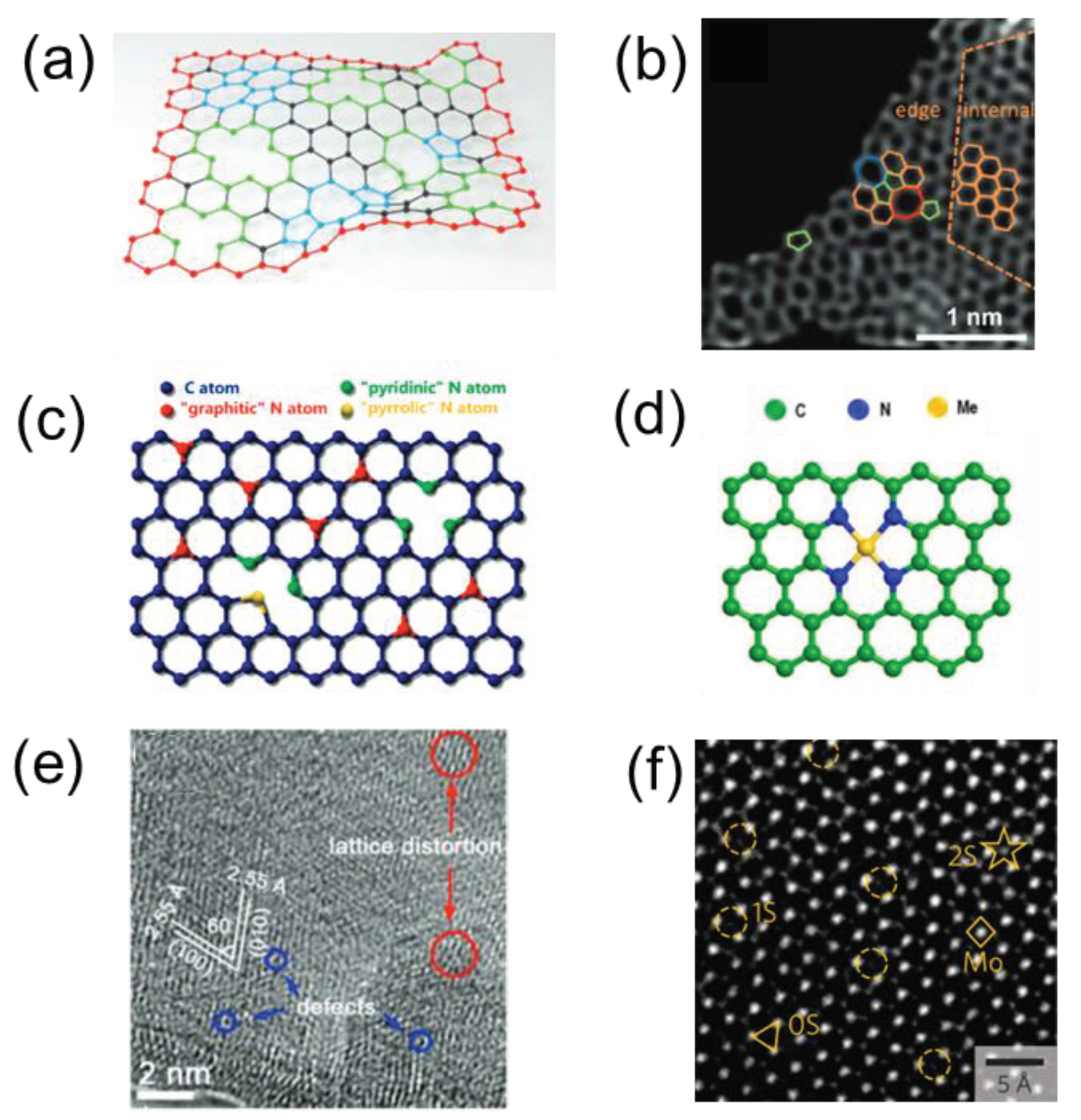
Figure 7.
Plasmon-based photocatalysts: (a) Energy flux (Poynting vectors) shown passing through plasmonic particles, where the red/blue is high/low electric field intensity. Reprinted with permission from [80], Copyright 2011, Royal Society of. (b) Normalized extinction spectra of spherical Ag, Au, and Cu nanoparticles. Reprinted with permission from (c) Normalized extinction spectra for Ag wire and cube and spheres nanoparticles. Reprinted by permission from [81]. Copyright 2011, Springer Nature Limited. (d) Localized SPR plasmon resonance electric field on a sphere. Reprinted with permission from [82], Copyright 2017, American Chemical Society. (e) Pure metal plasmonic photocatalysis. Reprinted with permission from [83]. Copyright 2013, Royal Society of Chemistry (f). Major processes in plasmonic photocatalysis. Reprinted with permission from [77].
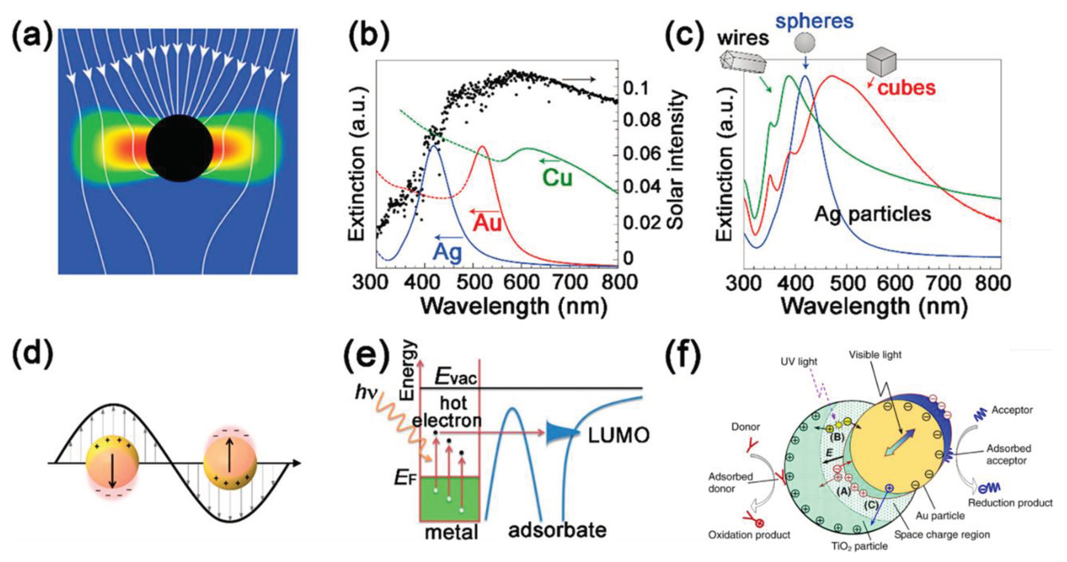
Figure 8.
(a) Mass spectra obtained by high-pressure photon ionization (HPPI)-TOFMS during the photodegradation of PS. (b) DRIFTS study of PS at different time intervals. Reprinted with permission from [89]. © 2020 Elsevier Inc. (c) Localized nanoscale AFM-IR spectra of nano-TiO2 coated polypropylene microplastics after photo-aging for different time periods; (d) Topographical images of TiO2 coated MPs after photocatalytic aging for 2 h; (e) AFM-IR spectra at different positions on the surface of MPs. Reprinted with permission from [94]. © 2020 Published by Elsevier B.V.
Disclaimer/Publisher’s Note: The statements, opinions and data contained in all publications are solely those of the individual author(s) and contributor(s) and not of MDPI and/or the editor(s). MDPI and/or the editor(s) disclaim responsibility for any injury to people or property resulting from any ideas, methods, instructions or products referred to in the content. |
© 2024 by the authors. Licensee MDPI, Basel, Switzerland. This article is an open access article distributed under the terms and conditions of the Creative Commons Attribution (CC BY) license (http://creativecommons.org/licenses/by/4.0/).
Copyright: This open access article is published under a Creative Commons CC BY 4.0 license, which permit the free download, distribution, and reuse, provided that the author and preprint are cited in any reuse.


