Submitted:
21 March 2024
Posted:
21 March 2024
You are already at the latest version
Abstract
To reduce the redundant counting of TDC in high-speed applications and thus reduce power consumption, a TDC architecture is proposed to quantify the difference between two adjacent rows of pixel signals. This structure can remove the identical part between two rows of pixel signals by adjusting the start and stop signal of the TDC, which will reduce the number of flipping of D flip-flops in the TDC. In the 110nm CMOS process, simulation results show that this design achieves an effective number of bits (ENOB) of 4.72 bits and a Figure of Merit (FoM) of 104.7 fJ/step - 162.3 fJ/step with a power consumption ranging from 60 µW to 93 µW. Compared with traditional counting methods, the proposed TDC can reduce counting power consumption by 30%.
Keywords:
Time-to-digital converters
; Image sensors
; Low power consumption
; High-speed
1. Introduction
A time-to-digital converter (TDC) is a circuit that measures the time difference between two input events or pulse widths and is widely used in devices such as laser rangefinders, true random number generators, time-of-flight measurements, positron emission tomography scanners, and all digital phase-locked loops (AD PLL). There are many architectures for high resolution TDC, including a vernier based delay chain TDC[1], a time-amplifier based TDC[2,3], and a gated ring oscillator (GRO) TDC[4]. Pure digital TDC based on a delay chain has the advantages of high throughput and simple structure[5], therefore, it is increasingly appearing in various applications.
The surge in high-speed computing tasks — ranging from target tracking and machine vision to scientific exploration — has escalated the need for advanced image sensors characterized by superior frame rates and responsiveness. Single Slope (SS) Analog-to-Digital Converters (ADCs), integrated with TDCs, emerge as a promising solution for enhancing CMOS image sensors’ speed without compromising image quality[6,7,8]. Nonetheless, the conventional delay chain-based TDCs face challenges of escalated power consumption and physical size with the expansion of quantization levels[9].
Ref. [10] uses gated delay technology to reduce power consumption, and Ref. [11] uses histogram memory instead of an analog counter to achieve the 3,300-fold power reduction. A low-power TDC structure is described in Ref. [12], which takes advantage of the continuity of analog signals in time. In this work, a new TDC structure applied to CMOS image sensors will be proposed by taking advantage of the continuity of analog signals in space. This structure will quantize two rows of the pixel signal of CMOS image sensor at the same time, and the same redundant data quantized between the two rows of the signal will be removed, which will reduce the flipping times of D flip-flop on the delay chain, thus reducing the counting power consumption by more than 30%.
2. Proposed Structure
2.1. Traditional Structure
The Single Slope ADC traditionally comprises a comparator, ramp generator, and counter. The ramp generator initiates a gradually decreasing voltage signal, with the counter tallying from the onset of this ramp. The pixel output is then compared to this slope voltage, yielding the SS ADC’s quantization result after decoding.
At higher quantization bits, the quantization speed of SS ADC will be affected due to the increase of slope length. While ensuring high quality and high integrity of image information, image sensors need to have a higher frame rate and faster response speed. Two-step SS ADC based on TDC can meet the needs of high-speed CMOS image sensors, and is increasingly used in the field of CMOS image sensors.
The working mode of the two-step SS ADC based on TDC is that the pixel signal will be compared with the ramp signal. When the pixel signal voltage is higher than the ramp voltage, the comparator will flip, and the output of the comparator will be coarse quantized by the post-feed counter, while the TDC will fine quantize the comparator flip signal. That is, the coarse quantization counts the number of clock cycles from the highest point of the ramp voltage to the comparator flip point, while the fine quantization quantifies the time from the comparator flip point to the end of its clock cycle. The two-step quantization method can effectively alleviate the energy consumption and load driving problems caused by too high clock frequency.
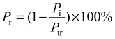
The comparator in SS ADC based on TDC usually adopts the fully differential comparator structure as shown in Figure 1. The working process is as follows: Switch S2 is closed, the two-stage comparator is reset, switch S1 is closed, and the voltage of Vin+ and Vin- is connected to the left plate of corresponding capacitor C1, respectively. When the voltage of Vin+ and Vin- is stabilized, S1 and S2 are disconnected. In order to inhibit the channel charge injection of the S2 switch, the turn-off time of S1 is 4 ns later than that of S2. The input signal is then quantized, and the second level comparator converts the double-ended output into a single-ended output.
The structure of the single-stage comparator in a fully differential two-stage comparator is shown in Figure 2. Considering the input common model envelope of the comparator input signal, the differential input pair tube adopts a PMOS transistor. Assuming that Vin+ and Vin- are common-mode signals when the comparator starts to work, if Vin+ increases and Vin- decreases, the overdrive voltage of the M3 transistor will decrease, the leakage current will decrease, and the leakage current of the M4 transistor will increase. Because the gate leakage of M5 and M8 transistors are connected, they are always in the saturation region, and the change of current will reduce the gate voltage of M5 transistor. That is, when Vin- decreases, the gate voltage of M8 transistors increases, that is, Vin+ increases. At the same time, the gate voltage of M6 and M7 transistors is controlled by Vin+ and Vin- respectively. Therefore, the increase of Vin+ will increase the leakage current of M6 transistors, thus making M6 distribute more current, which makes the leakage current of M5 transistors smaller, and its gate voltage further decreases, forming a positive feedback. Similarly, the gate voltage of the M8 transistor will further increase, and finally, M6 will enter the deep linear region, M7 will enter the cut-off region, the comparator will complete the comparison, Vin+ output high level, and Vin- output low level.
The traditional TDC structure for CMOS image sensors is shown in Figure 3, which is mainly composed of a delayed phase-locked loop, delay chain and D-flip-flop. The pixel output is transmitted to the column level for comparison with the reference ramp, and the point in time at which the comparator flips is transmitted to the delay-locked loop (DLL) delay chain. 2n delay units are required to complete n-bit quantization. The rising edge of the comparator flip is delayed by each delay unit with the same time accuracy, and the output of each delay unit is connected to the signal input of the D flip-flop. The rising edge of the next clock cycle will be sent to the clock input of the D flip-flop as a stop signal. The clock signal will sample the signal input of the D flip-flop and read the output of the delay unit into the D flip-flop. Then the D flip-flop is used as a shift register, the data in the D flip-flop is passed to the decoder, and the final N-bit quantization result is obtained.
The main power consumption of TDC comes from the power consumption of the delay unit and the D flip-flop, where the delay unit ensures the accuracy of the delay time, and its current size is determined by the Vctrl provided by the DLL. The power consumption of CMOS circuit is
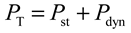 where PT is the total power consumption, Pst is the static power consumption, and Pdyn is the dynamic power consumption. Static power consumption is mainly caused by drain current, and static power consumption is
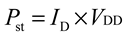 where, ID is drain current and VDD is power supply voltage. Dynamic power consumption is mainly caused by the charge and discharge of the circuit to the node capacitor. Each charge (or discharge) of a node capacitor C will lead to the dynamic power consumption of 1/2CVDD2. Therefore, the average static power consumption of a node i in the circuit during the whole working time can be expressed as [13]
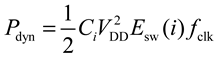 where, fclk is the clock frequency and Esw is the switching activity, which represents the average number of jumps of the node i signal in each clock cycle. Therefore, the more the number of signal jumps of the D flip-flop, the higher its dynamic power consumption, resulting in a higher total power consumption.
In the simulation process, it can be found that when the signal input of the D flip-flop is kept at a low level, its power consumption level is far less than that when the signal input has a high level. Simulation of the D flip-flop we used is carried out, as shown in Figure 4, respectively, the current condition of the output of the D flip-flop becomes high level and the current condition of the input and output of the D flip-flop is kept low level. It was calculated through a calculator that the average current when the output remained low was 32.88 nA, while the average current when the output changed was 217.2 nA. It could be seen that the average current of D flip-flop would be significantly increased by flipping. The power consumption of D flip-flop was mainly the power consumption of its flipping. Therefore, if a new counting method is adopted to reduce the flipping times of the D flip-flop in TDC, low power consumption can be achieved.
The output of the delay chain in the quantization process is shown in Figure 5. Where Comp_outb1 and Comp_outb2 represent the inversion signal of the comparator in the first and second rows respectively, and DFF_in<N> represents the input of the NTH D flip-flop, which is the output of the NTH delay unit. When the stop signal arrives, each D flip-flop will sample the output of the delay unit and generate a thermometer code with 1 and 0 separated as 111…00. Due to the continuity of the analog signal, the light intensity information between the two adjacent rows of pixels is generally very close, so its quantization code value will also be very close. If a more simplified quantization method that quantizes the difference between two rows of pixel signals rather than the full signal can be adopted to eliminate the quantization of the same part between the two rows of signals, the quantification of redundant information will be removed. The number of output signals of 1 can be reduced, that is, the number of flips of the D flip-flop can be reduced, thus reducing the counting power consumption.
The main source of ADC differential nonlinearity is the random variation of the delay time of the delay unit buffer caused by the inconsistency and mismatch of the device manufacturing. The greater the number of delay buffers, the greater the differential nonlinearity, which will cause a certain error. In addition, the D flip-flop must ensure that it has a narrow metastable width, which must be shorter than the delay period of the delay unit, so as to reduce the TDC time measurement error.
2.2. Proposed TDC
The improved column-level readout architecture is shown in Figure 6. Since the output of two rows of pixels needs to be compared to quantify their difference, two column parallel buses need to be used for simultaneous readout, and the output of pixels is sent to the column-level comparator for comparison with the reference slope voltage respectively. When the output signals of the two rows of pixels are different, the flip time of the comparator will also be different. By sending the outputs of the two comparators into two sets of TDC for quantization at the same time, the flip time point of the comparator, that is, the output signal of the pixel, can be encoded.
In high-speed image sensors, considering the RC delay of the row driver signal transmission line and column bus, the row driver signal is difficult to be completed from the timing control driver circuit on both sides of the pixel array to the most middle column pixel in the row selection time, and the most middle row pixel signal is output to the column level through the column bus.
Under the premise of not reducing the pixel array and frame rate, to achieve complete signal transmission within the row time, the mode of simultaneous readout of two column buses proposed in this work can be adopted. Each column pixel shares two column buses, and the pixel output of odd and even rows is transmitted to the column level respectively. In this way, the timing control driver circuit can select two adjacent rows of pixels each time. The signal is selected and read at the same time, each column bus only needs to complete the selecting and reading of half of the pixel output in one frame time, and the row selection time can be doubled, which greatly alleviates the pressure of signal establishment in the row selection time. Therefore, the proposed TDC is very suitable for high-speed CMOS image sensors.
For TDC to quantify the difference between the output of two rows of pixels, it is necessary to quantify the time difference between the flip time points of the two rows of comparators. This work designs a series of logic circuits before TDC. The following purposes can be achieved by using the logic circuit as shown in Figure 7.
In the initial state disjunction gate output OR1 is high, when comp_out1, that is, the first-row comparator flip time point arrives earlier than comp_out2, disjunction gate output remains high, the output of multiplexer A is the delay of the first-row comparator flip invert signal, and the signal which will be delayed by the delayed chain is sent to the start signal input of the first row TDC. At this time, the clock input of D flip-flop has not yet arrived, and its output is the default value after reset, that is, the low level. The output of multiplexer B is also the delay of the first row of the comparator flipping invert signal, and the start signal of the two rows of TDC is the delay of the first row of the comparator flipping invert signal. After that, even if the second row of the comparator flipping time arrives, the value of OR1 remains unchanged. The output of the D flip-flop will also remain low; Since the output of the D flip-flop remains low, the stop signal of the first row TDC is the rising edge of the next clock cycle, and the stop signal of the second row TDC is the delay of the second row comparator flip invert signal.
When comp_out2 arrives before comp_out1, the output OR1 of the disjunction gate will become low, the output of multiplexer A will be the delay of the second row comparator flip invert signal, the output of the D flip-flop will also jump to a high level, and multiplexer B will select the delay of the second row comparator flip invert signal. At this time, the stop signal of the second row of TDC is the rising edge of the next clock cycle, and the stop signal of the first row of TDC is the delay of the first row of the comparator flip invert signal.
It can be seen that the first arrived comparator flip signal will be fully quantized the time from the flip time point to the rising edge of the next clock cycle, and the other row of TDC completes the quantization of the time difference between the flip points of the two rows of comparators. Due to the spatial continuity of the analog signal, the difference is usually relatively small. Therefore, this quantization method can reduce the number of flips of the D flip-flop, thereby reducing the power consumption of the count. In addition, in traditional TDC-based SS ADCs, an edge detection circuit is usually needed to generate a stop signal, that is, the comparator flip signal is delayed, and the D flip-flop is used to sample the end of the clock cycle where TDC quantization is located, that is, the rising edge of the next clock cycle. In the improved TDC, the stop signal of the faster row of the comparator flipping signal is the end of the whole quantization time, and the stop signal of the slower row of the comparator flipping signal is the stop signal of the other row of TDC. Therefore, the improved TDC does not need the edge detection circuit to provide the stop signal, which can further save power consumption. The TDC-based SS ADC used in Ref. [6], the edge detection circuit is usually needed to generate the stop signal, that is, the comparator flip signal is delayed, and the D flip-flop is used to sample the end of the clock cycle where the TDC quantization is located, that is, the rising edge of the next clock cycle. In the improved TDC, the stop signal of the faster row of the comparator flipping signal is the end of the whole quantization time, and the stop signal of the slower row of the comparator flipping signal is the stop signal of the other row of TDC. Therefore, the improved TDC does not need the edge detection circuit to provide the stop signal, which can further save power consumption.
3. Modeling Analysis
The low-power counting method introduced above is modeled and analyzed. The new counting model is used to quantify the image, and the gray value of the image is converted into the input signal of pixels. The analog-to-digital conversion model is established according to the improved working mode of TDC, and the gray value of every two rows is compared. Data with a larger gray value is quantified as the difference in code values between the two rows, The quantized part of the code value represents the number of flips of the D flip-flop, and the unquantized part is multiplied by the static power consumption of the D flip-flop, plus the power consumption of each logical unit to obtain the total power consumption. That is, the total power consumption is
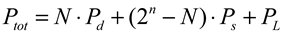 where, Ptot represents the total power consumption of TDC, N is the number of D-flip-flops with high output levels, n is the quantization bit, Pd and Ps represent respectively the flip power consumption and static power consumption of D-flip-flops, PL represents the power consumption of other logic circuits.
The power consumption reduction level of the improved counting mode is shown in Figure 8. The power consumption reduction level Pr is:
 where Pi represents the power consumption of the improved TDC, and Ptr represents the power consumption of the traditional structure.
The same part between the two rows of pixel signals is quantized only once, the number of flips of the D flip-flop is significantly reduced, and unnecessary redundant counts are removed. Compared with the traditional quantization method, the improved low-power counting method significantly reduces the power consumption. The higher the quantization accuracy, the more obvious the power consumption reduction level. When the quantization bit is 3, the low-power counting method can reduce the counting power consumption by more than 25%; when the quantization bit is further increased, the power consumption reduction degree tends to be stable, about 32%.
With the increase of quantization bits, the effect of the TDC power consumption reduction proposed in this paper will be more significant. However, the number of delay units and D-flip-flops in TDC is 2n, where n is the quantization bits of TDC. Therefore, with the increase of quantization bits, the number of delay units and D-flip-flops will increase exponentially and occupy a larger area; At the same time, under the condition of constant time precision, the length of the TDC delay chain determines the quantization time of TDC, and the increase of delay unit will make the delay chain longer, and then increase the quantization time of the TDC. Therefore, in order to control the area of TDC and improve the quantization speed, the TDC proposed in this paper is designed to be 5-bit. The number of delay units and D flip-flop is 32.
4. Simulition Results
The improved TDC simulation results are shown in Figure 9 (a), (b) and (c), respectively, when comp_out1 signal arrives first, when comp_out2 arrives first, and when comp_out1 and comp_out2 arrive simultaneously. The figure shows the result after transcoding the thermometer code of the TDC, where D1 represents the output of the TDC in odd rows, D2 represents the output of the TDC in even rows, and each flip indicates that the TDC outputs a “1”. It can be seen from the simulation results that the designed TDC can fully quantify the complement of the first arrived signal, and the other row of TDC can quantify the difference between the two rows of signals.
However, in the process of reducing the time accuracy of TDC, it is found that the multiplexer control signal at the input will pass through a D flip-flop before the start signal of the second row of TDC enters, resulting in a 350 ps delay of the start signal. When the time accuracy is less than 1ns, the delay effect is very significant. This will cause the TDC quantization to lose one number. In order to solve this problem, the stop signal in this case is delayed by the same means, that is, before the clock signal enters the TDC, the first stage D flip-flop is delayed. It is proved that this method can effectively reduce the quantization error of TDC.
However, when the proposed TDC structure is used as a fine quantization counter in a two-step SS ADC, if the two comparator flip points are in two different coarse quantization clock cycles, the number will be miscounted. Therefore, a judgment circuit or gate input is required to be the inverting output of the edge detection circuit, the stop signal of the current line and the output of the first D flip-flop. At the end of the coarse quantized clock cycle where the comparator flip point is reached first, that is, when the rising edge of the next clock cycle arrives, if the stop signal of the current line is still low at this time, It means that the two comparators do not flip in the same coarse quantization period, in this case, the start signal of the line receives the output of the comparator, and the stop signal receives the output of the edge detection circuit, in this case, the start signal will change from a high level to a low level, and the output result of the D flip-flop is the complement. In order to reduce this situation as much as possible, the quantization number of TDC can be as large as possible, which can make the coarse quantization clock cycle longer, and also alleviate the energy consumption problem caused by too high clock frequency to a certain extent.
In order to investigate the dynamic behavior of the proposed TDC, a full-scale sinusoidal input signal at 3.052 kHz is applied to the circuit and the analog equivalent of the output digital codes and its spectrum are calculated and depicted in Figure 10. Since the logic circuit before the odd-line and even-line TDC is slightly different, and therefore has a different spectrum, it can be observed that the signal-to-noise and distortion ratio(SNDR) of the odd-line TDC is 31.1628 dB, resulting in an effective number of bits(ENOB) of 4.88 bits. In addition, the spurious free dynamic range(SFDR) of the circuit is 43.5359 dB. The even-line TDC has a signal-to-noise and distortion ratio (SNDR) of 30.1704 dB, resulting in an effective number of bits(ENOB) of 4.72 bits, and a spurious-free dynamic range(SFDR) is 39.1755 dB.
Finally, Table 1 compares the performance of the proposed low-power structure with the other works. In Ref. [12], the value of the new sample signal is encoded according to the difference between the previous signal and the new sample signal, and the continuity of the analog signal in time is utilized to reduce the power consumption of the circuit. The proposed TDC uses the continuity of the analog signal in space to reduce the counting power consumption of TDC, and has a lower optimization coefficient FoM. In addition, the method of quantizing two rows of pixel output at the same time is more suitable for high-speed image sensor applications. Compared with TDC in two-step SS ADC applied to CMOS image sensor in Ref. [14], the proposed TDC has lower power consumption and FoM. Ref. [15] proposed a two-step TDC based on a time amplifier, in which only one time amplifier is activated at each conversion stage, so that TDC has better system energy efficiency. FoM of the proposed TDC has obvious advantages compared with it.
5. Conclusions
In this work, a new low-power TDC structure is proposed, which is mainly used for high-speed SS ADC of CMOS image sensors. The proposed TDC utilizes the continuity of analog signals between rows of image sensor pixels and quantifies the difference between the two adjacent rows of pixel outputs by adjusting the start and stop signal inputs of the all-digital TDC to reduce the number of flips of the D-flip-flop on the voltage controlled delay line.
Compared with traditional TDC, the two row TDC quantization can greatly relieve the pressure of high-speed image sensor row selection time and meet the needs of high-speed design. At the same time, it quantifies the difference between two rows of pixel signals rather than the complete pixel signal, so its counting power consumption is greatly reduced, when the quantization bit reaches 5 bits, its power consumption reduction level can reach more than 30%. The proposed TDC can achieve a FoM of 104.7 fJ/step - 162.3 fJ/step with a significant reduction in counting power consumption.
References
- Lu, P.; Wu, Y. A 90 nm CMOS digital PLL based on vernier-gated-ring-oscillator time-to-digital converter. In Proceedings of the IEEE International Symposium on Circuits and Systems (ISCAS); 2012; pp. 2593–2596. [Google Scholar] [CrossRef]
- Liu, J.; Hassanpourghadi, M.; Chen, M. A 10GS/s 8b 25fJ/c-s 2850μm2 two-step time-domain ADC using delay-tracking pipelined-SAR TDC with 500fs time step in 14 nm CMOS technology. In Proceedings of the International Solid-State Circuits Conference (ISSCC); 2022; pp. 160–162. [Google Scholar] [CrossRef]
- Yi, X.; Liang, Z.; Boon, C.; et al. An inverted ring oscillator noise-shaping time-to-digital converter with in-band noise reduction and coherent noise cancellation. IEEE Transactions on Circuits and Systems I Regular Papers 2020, 67, 686–698. [Google Scholar] [CrossRef]
- Teh, J.S.; Siek, L.A. 12-bit branching time-to-digital converter with power saving features and digital based resolution tuning for PVT variations. Analog Integr Circ Sig Process 2020, 105, 57–71. [Google Scholar] [CrossRef]
- Tangudu, J.; Gunturi, S.; Jalan, S.; et al. Quantization noise improvement of Time to Digital Converter (TDC) for ADPLL. In Proceedings of the 2009 IEEE International Symposium on Circuits and Systems; 2009. [Google Scholar] [CrossRef]
- Gao, J.; Yan, N.; Nie, K.; et al. A 2.44μs row conversion time 12-bit high-speed differential single-slope ADC with TDC applied to CMOS image sensor. Microelectronics Journal 2022, 120, 105322. [Google Scholar] [CrossRef]
- Levski, D.; Wäny, M.; Choubey, B. A 1- us Ramp Time 12-bit Column-Parallel Flash TDC-Interpolated Single-Slope ADC With Digital Delay-Element Calibration. IEEE Transactions on Circuits and Systems I Regular Papers 2019, 66, 54–67. [Google Scholar] [CrossRef]
- Wang, Y.; Guo, Z.; Guo, Y.; et al. High Speed Column Level ADC Design with TDC Technology for CMOS Image Sensor. In Proceedings of the 2023 6th International Conference on Electronics Technology (ICET), Chengdu; 2023; pp. 180–184. [Google Scholar] [CrossRef]
- Abdelmejeed, M.; Guindi, R.; Abdel-Moneum, M. A novel 10-Bit high-throughput two-stage TDC with reduced power and improved linearity. In Proceedings of the 2013 4th Annual International Conference on Energy Aware Computing Systems and Applications (ICEAC), Istanbul; 2013; pp. 50–54. [Google Scholar] [CrossRef]
- Zhang, F.; Tang, L.; Zhang, Y.; Tang, X.; et al. A Low-Power Two-Step Time-to-Digital Conversion in 28 nm CMOS. In Proceedings of the 2022 7th International Conference on Integrated Circuits and Microsystems (ICICM); 2022; pp. 570–573. [Google Scholar] [CrossRef]
- Han, S.H.; et al. A 100×80 CMOS Flash LiDAR Sensor with 0.0011mm2 In-Pixel Histogramming TDC Based on Analog Counter and Self-Calibrated Single-Slope ADC. In Proceedings of the 2022 IEEE Symposium on VLSI Technology and Circuits (VLSI Technology and Circuits); 2022; pp. 82–83. [Google Scholar] [CrossRef]
- Rostami, M.S.; Saberi, M.; Maymandi-Nejad, M.; et al. A Low-Power Time-to-Digital Converter for Sensor Interface Circuits. IEEE Transactions on Circuits and Systems II Express Briefs 2020, 67, 2853–2857. [Google Scholar] [CrossRef]
- Pedram, M. Power Minimization in IC Design: Principles and Applications. ACM Transactions on Design Automation 1996, 1, 3–56. [Google Scholar] [CrossRef]
- Wang, G.; Chen, Q.; Xu, J.; et al. 2μs row time 12-bit column-parallel single slope ADC for high-speed CMOS image sensor. Microelectronics Journal 2023, 135, 105768. [Google Scholar] [CrossRef]
- Molaei, H.; Hajsadeghi, K. A 5.3-ps, 8-b Time to Digital Converter Using a New Gain-Reconfigurable Time Amplifier. IEEE Transactions on Circuits and Systems 2019, 66, 352–356. [Google Scholar] [CrossRef]
Figure 1.
Fully Differential comparator.
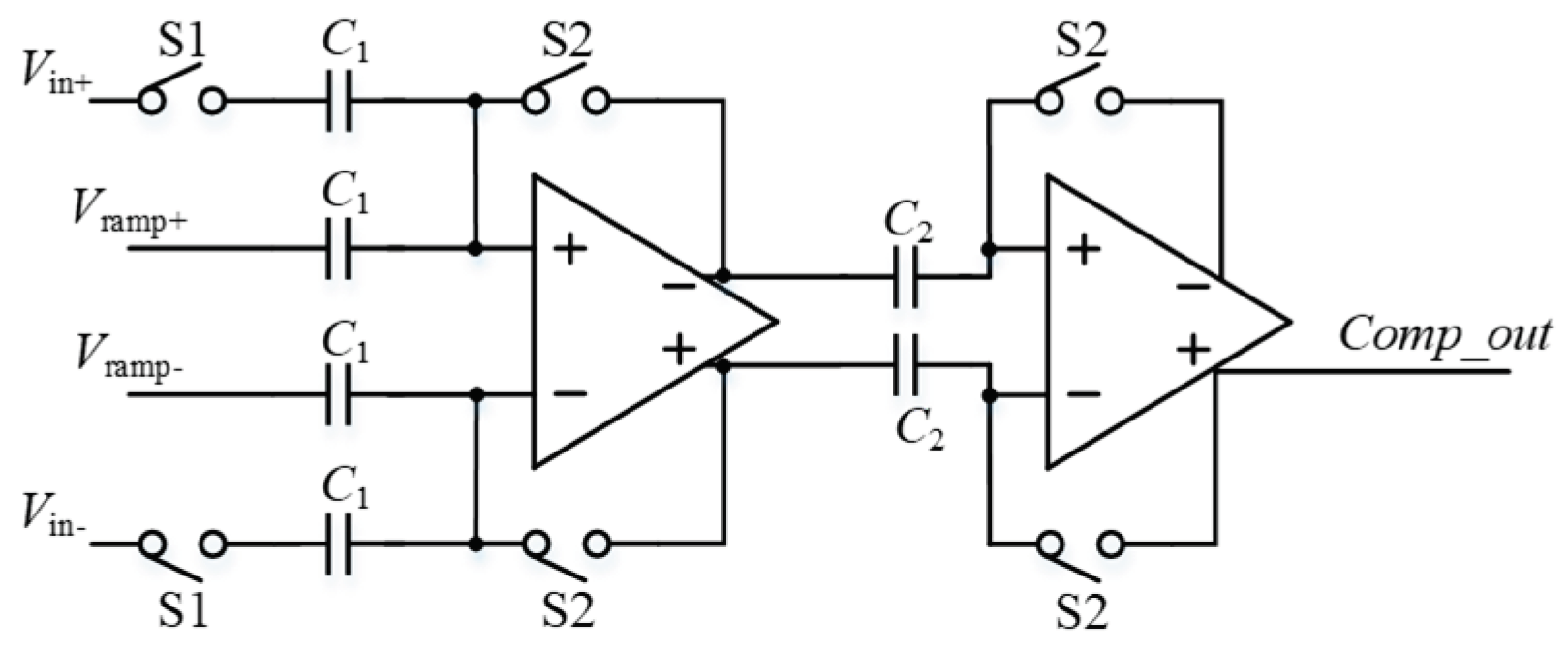
Figure 2.
Single-stage comparator.
Figure 3.
TDC structure based on delay chain.
Figure 4.
D Current status of the flip-flop output with or without jumping.
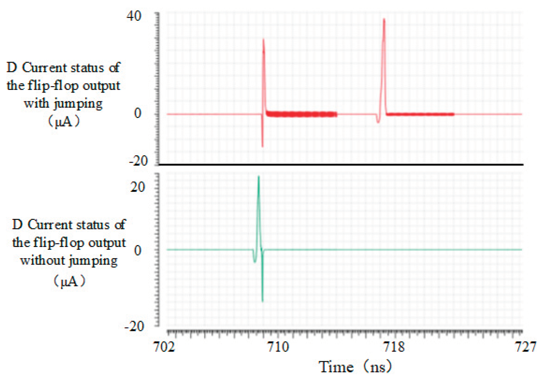
Figure 5.
The output of the delay chain in the quantization process.
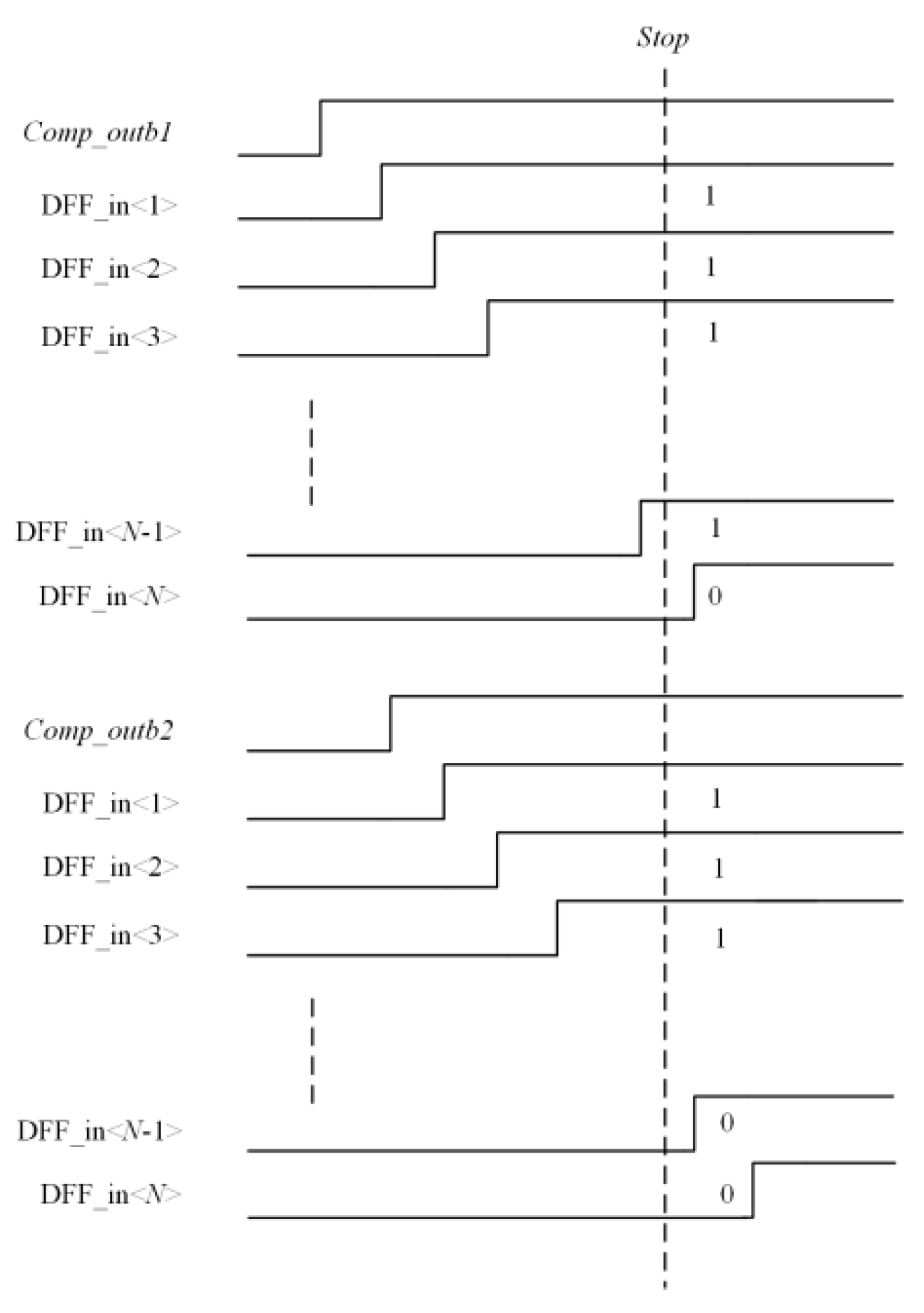
Figure 6.
Improved post-column level readout architecture.
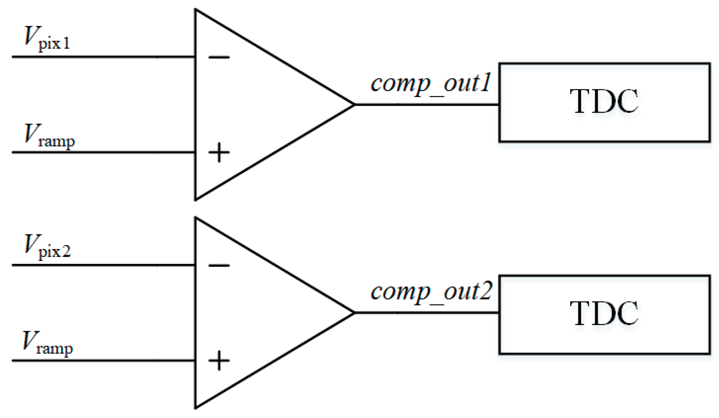
Figure 7.
Improved TDC front logic circuit.
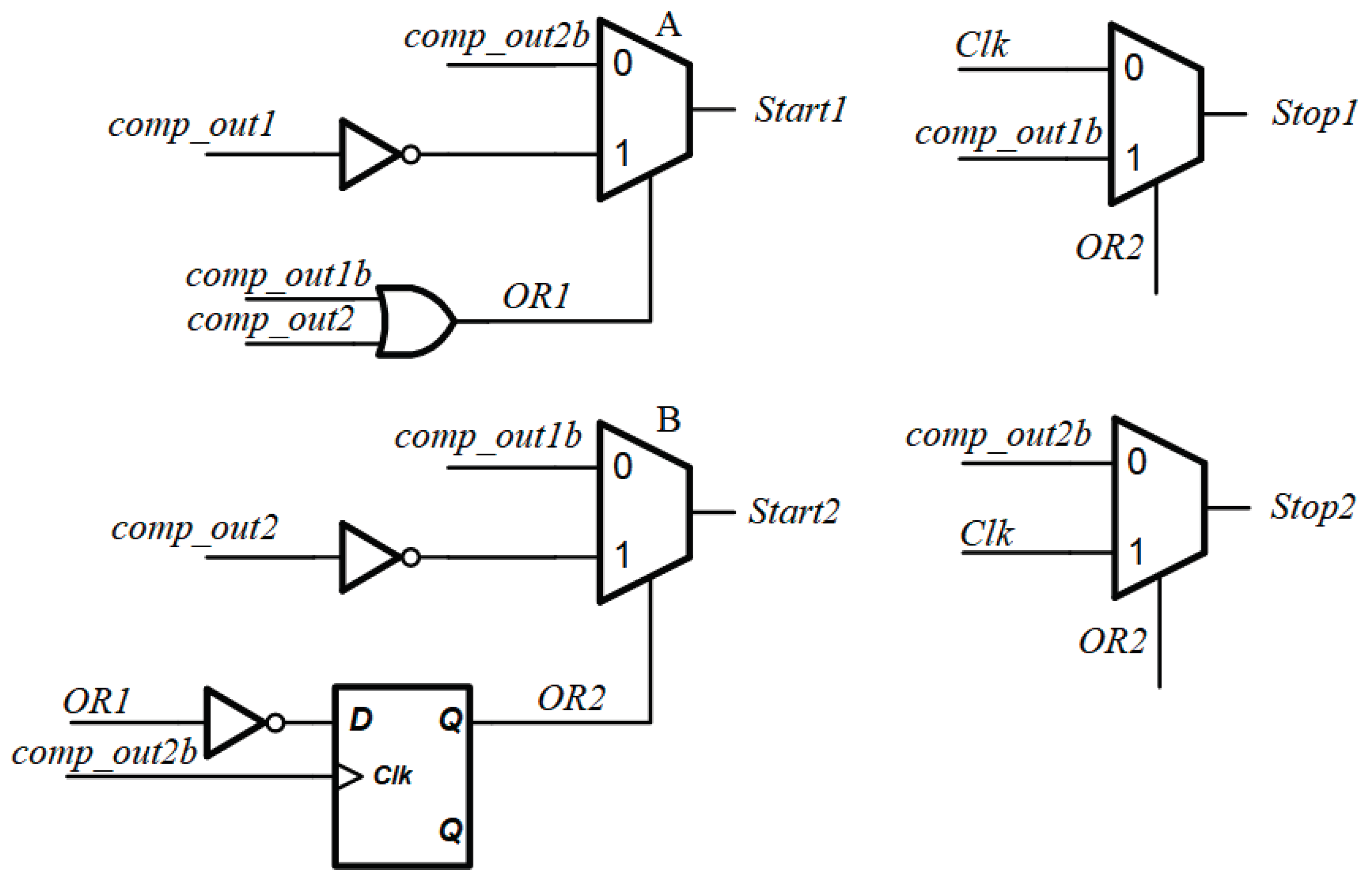
Figure 8.
The power consumption of the improved counting model is reduced.
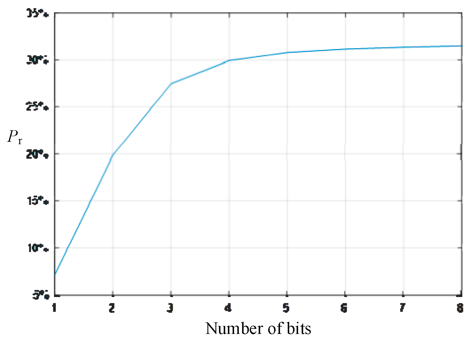
Figure 9.
Functional simulation of TDC in different situations.
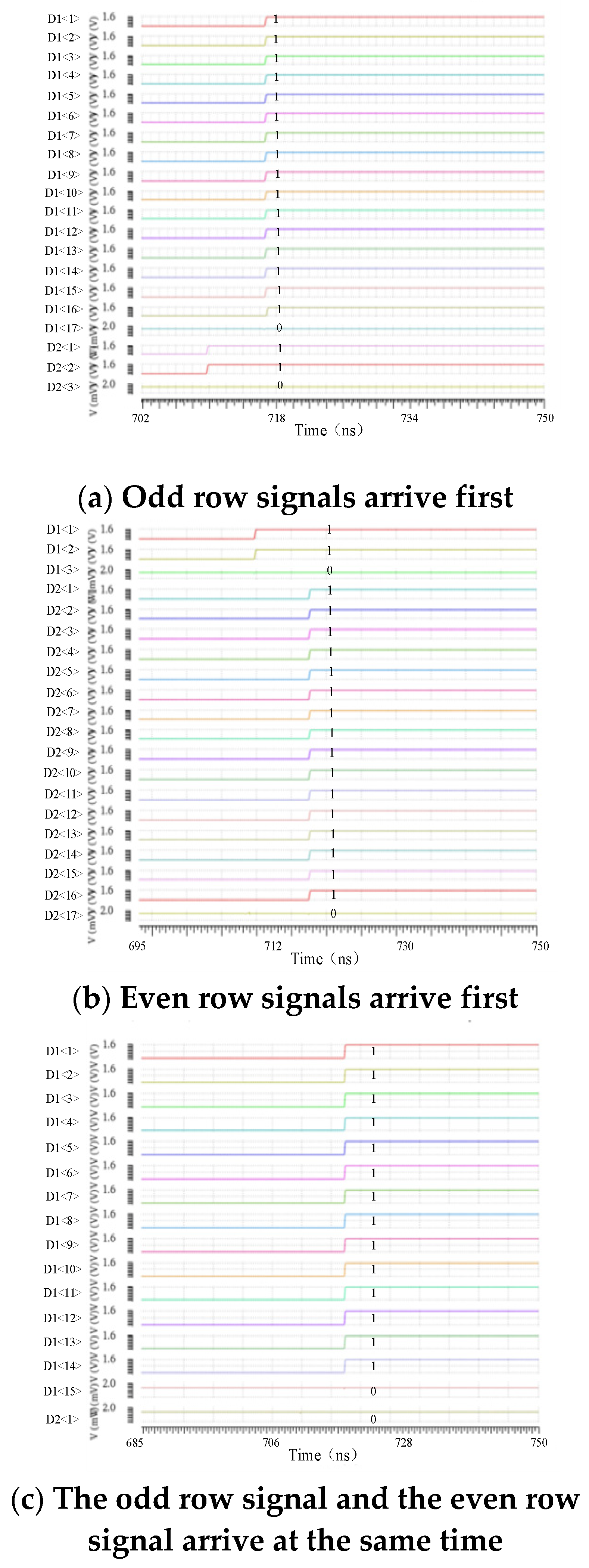
Figure 10.
Functional simulation of TDC.
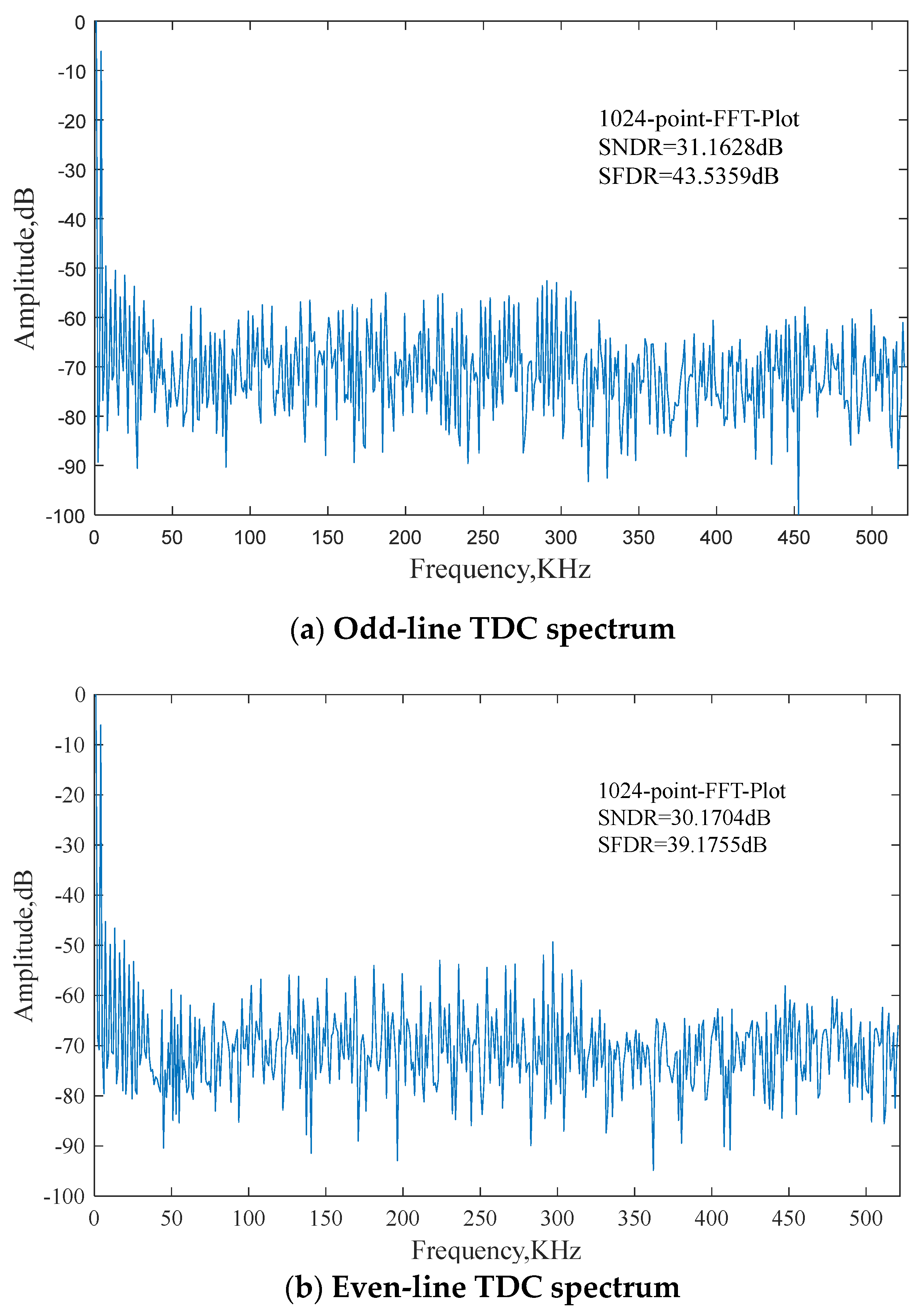

Table 1.
Performance comparison of the proposed TDC structure with the other works.
| [12] | [14] | [15] | This work | |
|---|---|---|---|---|
| CMOS process | 65nm | 0.11μm | 0.18μm | 0.11μm |
| Number of bits | 8 | 12 | 8 | 5 |
| Sampling rate(MS/s) | 0.2 | 0.5 | 30 | 20 |
| Power(μW) | 10 | 187 | 1100 | 60-93 |
| ENOB(bits) | 7.52 | 10.68 | 6.07 | 4.72 |
| FoM*(fJ/step) | 275.0 | 182.6 | 540.0 | 104.7-162.3 |
*FoM=(Power×1 Row Time)/2ENOB.
Disclaimer/Publisher’s Note: The statements, opinions and data contained in all publications are solely those of the individual author(s) and contributor(s) and not of MDPI and/or the editor(s). MDPI and/or the editor(s) disclaim responsibility for any injury to people or property resulting from any ideas, methods, instructions or products referred to in the content. |
© 2024 by the authors. Licensee MDPI, Basel, Switzerland. This article is an open access article distributed under the terms and conditions of the Creative Commons Attribution (CC BY) license (http://creativecommons.org/licenses/by/4.0/).
Copyright: This open access article is published under a Creative Commons CC BY 4.0 license, which permit the free download, distribution, and reuse, provided that the author and preprint are cited in any reuse.


