1. Introduction
In nanophotonics, scientists are primarily concerned with researching various methods and structures that are capable of enhancing and confining light in nanoscale geometries. To this end, plasmonic has attracted considerable attention due to its ability to manipulate and control light at the nanoscale, leading to improved performance in sensing, imaging, energy harvesting and other technological applications. [
1,
2,
3,
4]. The unique properties of plasmonic structures offer researchers a versatile toolbox for addressing the challenges and opportunities presented in the field of nanophotonics
Recently, an alternative plasmonic system known as nanoparticle-on-mirror (NPOM) or film-coupled nanoparticle system has attracted much attention in the field of plasmonic [
4,
5,
6,
7,
8,
9,
10,
11]. The key feature of such structures is the coupling of the dipole generated in the nanoparticle with its induced image dipole in the metal layer, which leads to the generation of a hotspot in the gap layer [
4,
8,
12]. This hotspot shows a strong enhancement of the electric field, which is confined to an area of a few nanometers thickness. So far, it has been shown that the plasmonic response of the NPOM system depends on many factors, ranging from the thickness of the dielectric spacer and the angle of incidence to the surrounding medium, the size of the NP and its spacing [
2,
5,
7,
13,
14]. The main advantage of such structures is the easy control of the thickness of the gap layer in which the hotspots are created compared to the spacing of the nanoparticles in conventional localized surface plasmon resonances created between the metal nanoparticles in plasmonic structures [
15]. However, metal nanoparticles tend to aggregate, which can affect their plasmonic properties and stability over time.
On the other hand, the plasmonic resonances in periodic metallic nanostructures can be precisely controlled by adjusting their dimensions (e.g., width, length, thickness). This tunability enables fine-tuning of the spectral response to the specific requirements of the sensor application. Periodic metallic nanostructures consisting of metal nanostrip arrays have the advantage of being less prone to aggregation and offer better long-term stability and reliability, especially in sensing applications. Such structures can be fabricated using advanced nanofabrication techniques such as electron beam lithography or focused ion beam milling [
16]. Metallic nanostrips can offer a higher signal-to-noise ratio due to their larger size and stronger plasmonic resonances. This increased signal strength makes it easier to distinguish between the desired signal and background noise, leading to more accurate and reliable measurement results. The size and position of the nanostrips can be precisely controlled, leading to easy control of the location of the hotspots created in the gap layer and the resulting enhancement of the electric field. This spatial control is advantageous for applications where specific regions or molecules need to be targeted. By adjusting the distance between the metal nanostrips and the metal layer, it is possible to control plasmonic coupling effects that can further enhance sensing capabilities and tailor the response of the sensor to specific analytes. The integration of nanoscale features with mirrors and dielectric layers provides a versatile platform for tailoring the interactions between light and matter [
17]. Furthermore, the anisotropic nature of nanostrips with plasmonic modes aligned along their length can provide additional design flexibility for specific applications, especially when directional plasmonic responses are desired. All these advantages of metal nanostrips and the fact that less attention has been paid to this periodic nanostructure in recent research have led us to design and explore a plasmonic structure with periodic metal nanostrips coupled to a mirror separated by an ultrathin dielectric interlayer [
18,
19].
Metallic nanodisk arrays could also be considered as an interesting periodic metallic nanostructure. Such a structure has all the advantages of metal nanostrip arrays plus a unique plasmonic behavior due to its circular morphology. Periodic metallic nanodisks have applications in various fields, including surface-enhanced spectroscopy, sensing and imaging. The strong local field enhancement around each nanodisk makes them particularly useful for the amplification of light-matter interactions. Understanding the differences in electric field enhancement and optical mode properties between different configurations is crucial for optimizing performance in various applications, such as improving light-matter coupling in sensors or improving efficiency in energy conversion devices.
Such structures exhibit a wide variety of plasmonic modes that determine their optical properties [
20,
21,
22,
23,
24]. Plasmonic modes refer to the collective oscillations of electrons at the metal-dielectric interface, which lead to resonances that strongly influence the interaction of light with these structures. Analysing these modes is the key to unlocking the secrets hidden in the resonant modes of plasmonic structures. Basically, there are two groups of modes in plasmonic structures: bright modes and dark modes. bright modes refer to the strong interaction of the structure with the incident light from outside [
21,
25]. Dark modes, on the other hand, refer to the weak interaction with the incident light [
26,
27]. The coexistence of dark and light plasmonic modes in metallic nanostructures leads to a diverse interplay that can be used for innovative applications. In certain structures, dark modes can be coupled with bright modes, resulting in hybrid modes with unique properties. This synergy enables the enhancement of interactions in both the near and far field and offers opportunities for advances in sensing, imaging and energy conversion.
To address the mentioned dilemma, this work aims to propose two structures with two different periodic nanostructures and to simulate their optical behavior as three-dimensional models using the software tool COMSOL Multiphysics. Both structures consist of a glass substrate, a gold film deposited on the substrate and a periodic nanostructure of gold (nanostrips and nanodisks) separated from the gold film by an ultrathin dielectric Al2O3 layer. The optical responses such as the enhancement of the electric field and the scattering, the absorption and the extinction cross-section of the two structures are investigated and compared. Two plasmonic resonance wavelengths were observed for both structures, which are related to different types of plasmonic modes such as the bright and dark modes or a combination of both, which is explained in the discussion. The results show that both structures are useful for field enhancement applications and that the structure with the periodic metal nanodisk array can achieve stronger field enhancement as well as larger absorption, extinction, and scattering cross sections at its dipole resonance wavelength, which is defined as the bright plasmonic mode. One of the main proposes of this comparative study is exploring the differences of these two structures in 3D modeling, while they assumed as the same structures in 2D modeling.
2. Materials and Methods
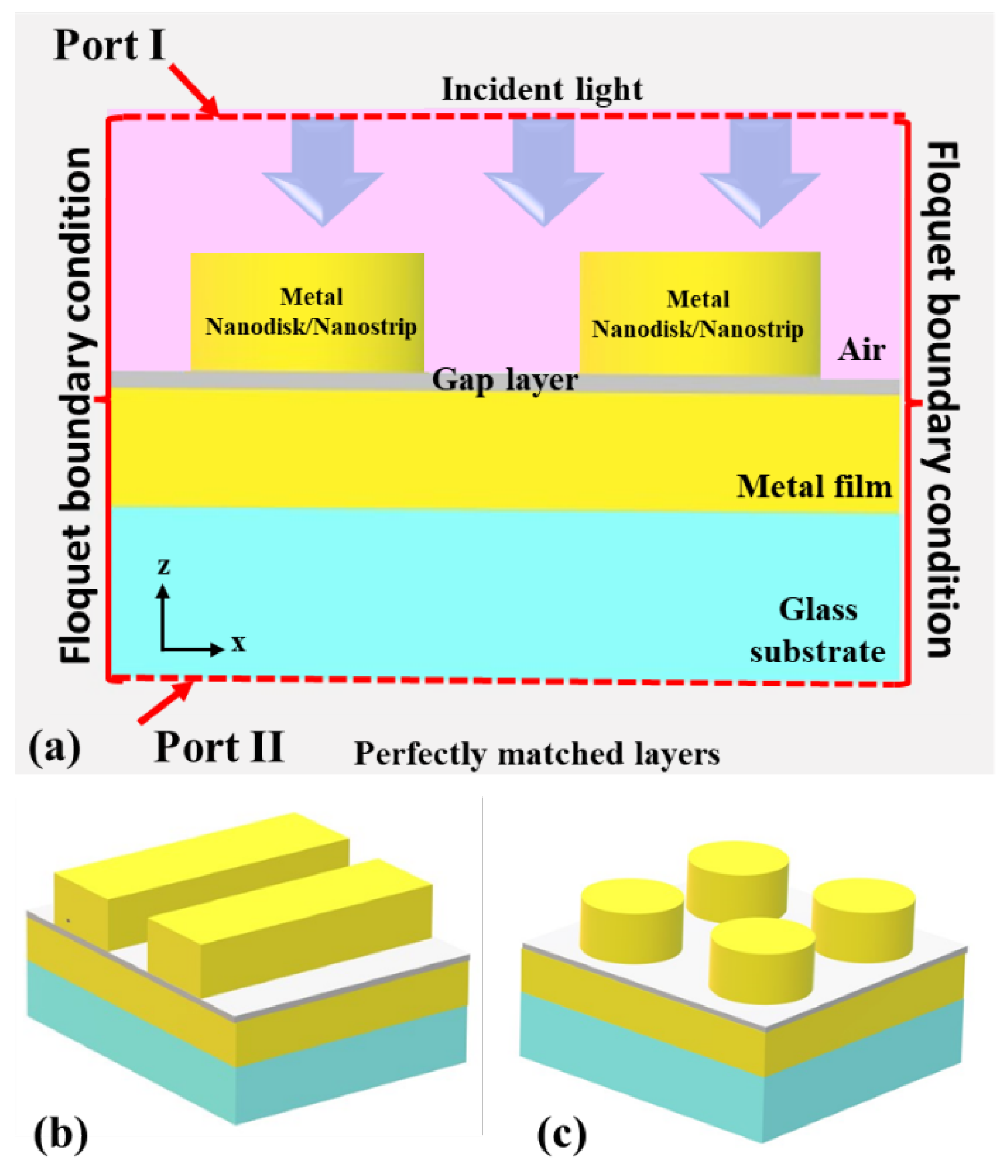
Three-dimensional electrodynamic calculations using the finite element method (FEM) in the Wave Optics module of COMSOL Multiphysics software tool are performed to design and simulate the optical response of the structures shown in
Figure 1.
Typically, the proposed structures consist of Au nanodisks/strips located above a metal mirror and separated by an ultrathin dielectric Al
2O
3 gap layer, as schematically illustrated in
Figure 1a. The mirror is 20 nm thick and can be deposited on the substrate by various deposition methods such as physical vapor deposition, while the Al
2O
3 layer is only 3 nm thick and can only be deposited directly on the mirror by atomic layer deposition (ALD). The height of the nanostrips and nanodisks is 30 nm and the diameter and width of the nanodisks and nanostrips are fixed at 80 nm. The depth of the nanostrip corresponds to the depth of the cell and is assumed to be infinite due to the Floquet periodic boundary condition. The distance between the nanodisks and the nanostrips is 40 nm, which is large enough to reduce the effects of coupling of the localized surface plasmons in this region. As mentioned above, metallic periodic nanostructures can be fabricated by advanced nanofabrication techniques such as electron beam lithography.
In the simulation, illumination is provided from the side of the nanodisks/strips that is perpendicular to the mirror. The incident light is set in the optics module as a full-field electromagnetic source, while the scattered light is set as a scattered-field electromagnetic source. The amplitude of the incident light is set to (1,0,0). The model uses n
a=1 for air and n
b=1.5 for the dielectric substrate. The metallic part of the structure is made of gold and its refractive index was taken from the Optical Materials Database. The refractive index of the dielectric Al
2O
3 interface is derived from the website refractiveindex.info as a function of wavelength (Boidin et al. 2016, thin film, n 0.3-18µm). The periodic Floquet boundary condition (FPBC) was applied to all plane boundaries along the z-axis of the structure to fulfil the “semi-infinite” condition for the excitation of LSPRs. This condition assumes that the model is infinite and the designed unit cell repeats periodically in the plane of the gold film. As shown in
Figure 1, perfectly matched layers are added around the structures to absorb electromagnetic waves and prevent reflections that would interfere with the simulation.
The near-field intensity gain maps are created by dividing the normalized scattered electric field strength by the normalized incident electric field in the gap layer as follows [
28,
29]:
Where V is the volume of the gap layer. The scattering, absorption and extinction cross sections of the periodic nanostructures are measured in the model. The scattering cross section is defined as [
30]
Here n is the normal vector pointing outward from the nanodisks/nanostrips, S
SC is the vector of scattered intensity (Poynting) and I
0 is the incident intensity, which is 1 MW/m
2. The integral is formed over the closed surface S of the nanoplate and the nanostrip. The absorption cross-section is equal to [
30]
where Q is the power loss density in the particle and the integral is taken over its volume. The extinction cross-section is simply the sum of the other two [
30,
31]:
3. Result and Discussion
The enhancement of the electric field in plasmonic structures is of great importance due to its diverse applications and effects. The enhancement of the electric field is particularly evident in the near-field region, close to the surface of the plasmonic structures. By comparing this quantity in different plasmonic structures, researchers and engineers can gain insights into the underlying physics and identify optimal designs for specific applications. In
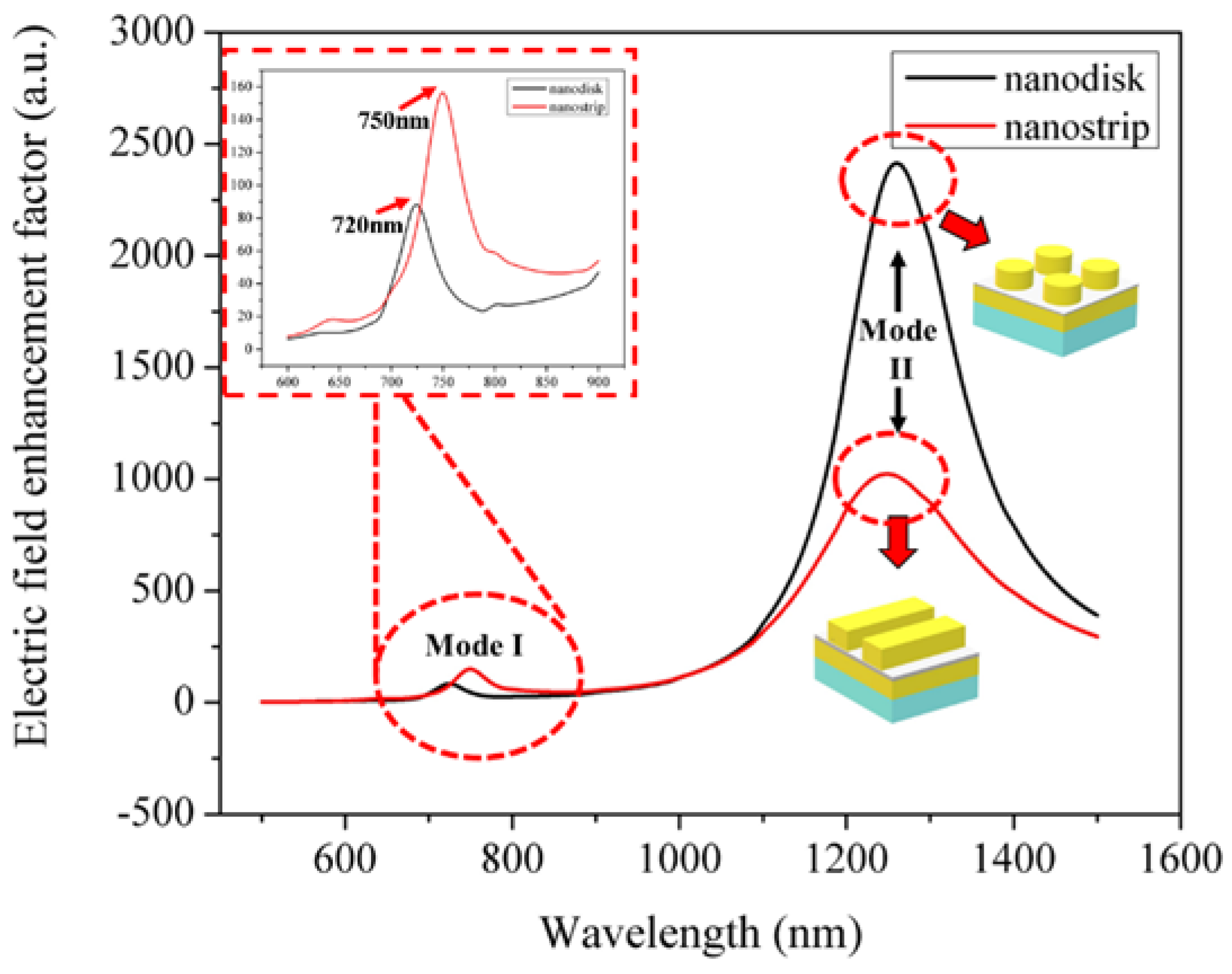
Figure 2, the electric field enhancement factor of the two structures with metallic nanodisk and nanostrip arrays is shown and compared. The electric field enhancement is calculated using Equation (1).
As shown in
Figure 2, both structures have two resonant modes in their gap layers, Mode I and Mode II. Mode I, indicated by the dashed circle in the graph, corresponds to the plasmonic resonance observed at shorter wavelengths for the nanostrip and nanodisk arrays. These are likely to be higher order modes or a combination of them, which may be more localized and have smaller enhancement factors compared to the fundamental mode. The inset in
Figure 2 shows an enlarged view of the resonance peaks related to Mode I for the nanostrip and nanodisk arrays, highlighting the details of the different modes and their respective wavelengths.
Mode II, indicated by the solid arrow, corresponds to the main plasmonic resonance peak, which is the dipolar plasmonic mode for the nanostrip array at 1250 nm and for the nanodisk array at 1260 nm. These resonances are stronger and more pronounced than the resonances at shorter wavelengths. The nanodisk structure shows a very large peak in the electric field enhancement factor at mode II compared to the nanostrip array. This indicates that the nanodisk array exhibits a strong plasmonic resonance at this wavelength, which significantly enhances the local electric field. The sharpness of the peak indicates that the resonance is well defined, which is typical for disk-shaped structures. This mode is typically the fundamental plasmonic resonance for such geometries. In other words, the reason for the difference in the electric field enhancement of the presented structures at mode II could be related to the geometry of the nanodisks, which allows a more efficient interaction with the incident light, leading to an enhanced coupling with the localized surface plasmons and thus a stronger field enhancement. The cross-sectional area for plasmon resonance in nanodisks is often larger than that in nanostrips, providing more opportunities for interaction with incident light and enhancement of the electric field.
The differences in the plasmonic behavior of the nanodisk and nanostrip arrays can be used for various applications, e.g., in sensor technology, where the sensitivity can be adjusted by selecting the appropriate structure and wavelength for the resonance. The larger enhancement factors are particularly useful in applications requiring strong field strengths, such as surface-enhanced Raman scattering (SERS) or amplified photodetectors.
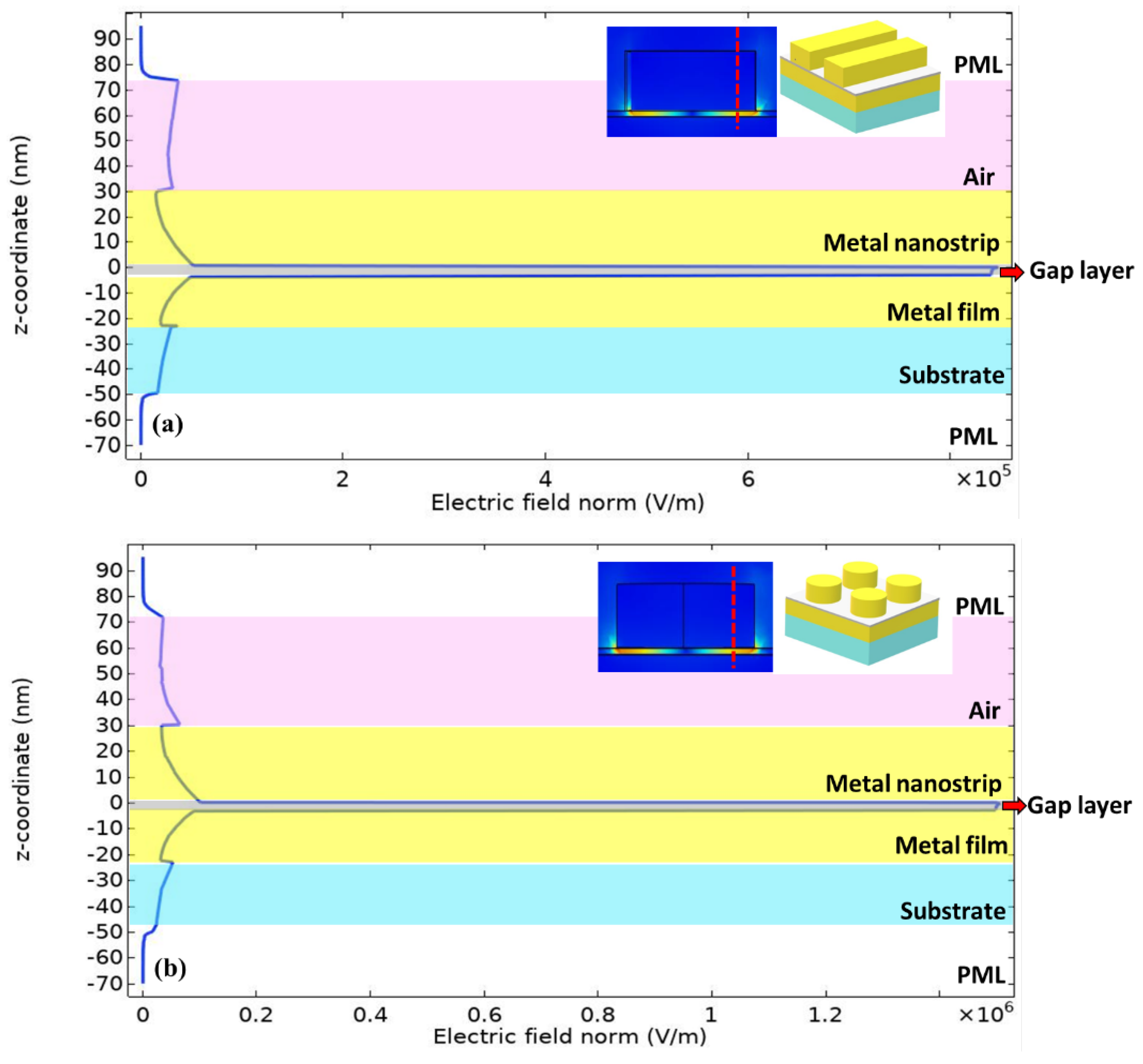
To investigate the variation of the electric field at mode II, inside each structure from port I to port II, the normalized electric field was simulated along a cut line passing through each structure at its dipole resonance wavelength, and the result is shown in
Figure 3a,b. The normalized electric field distribution of the structure at mode II are shown in inset pictures for each case and the red dashed lined in the inset pictures are the line that electric field is simulated along them. As shown, the normalized electric field in the air region above the nanostrip and metal nanoplate is relatively low, which is typical for a region without plasmonic structures to enhance the field. At the air-metal interface, there is a slight increase in the normalized electric field. This increase is indicative of the generated localized surface plasmon resonance (LSPR) around the nanostrip/nanodisk, where the oscillation of free electrons on the metal’s surface leads to a localized enhancement of the electric field. The electric field within the metal nanostrip itself is quickly attenuated due to the metal’s high electrical conductivity, which screens the electric field. Within the metal film, the normalized electric field is also very low, similar to within the nanostrip/nanodisk, due to the same high conductivity of the metal. As shown in both pictures a and b, the maximum magnitude of normalized electric field is confined in the dielectric gap layer between the metal film and metallic nanoarrays. As it is explained in the previous literatures, this strong electric field is due to the coupling of the localized surface plasmon resonances at this area. One way to compare the electric field in two structures could be a comparison of the normalized electric field in the gap layer for them. As it is obvious, normalized electric field for the structure with nanodisk array is larger than 1.3*10
6 V/m, but this amount is around of 7*10
5 V/m in the structure with nanostrip arrays. This result proves the result derived from
Figure 2 that shows the structure with metal nanodisk has stronger dipole mode and consequently stronger electric field enhancement at this mode.
After the light has penetrated the metal film, there is a slight increase in the electric field within the substrate compared to the metal film. This is probably due to the different material properties of the substrate, which allow the electric field to penetrate deeper. The normalized electric field drops steeply to zero when entering the perfectly matched layer (PML) region. This is to be expected as the PML is designed to absorb incoming electromagnetic waves to prevent reflection back into the simulation region, thus simulating an open boundary condition.
As shown in
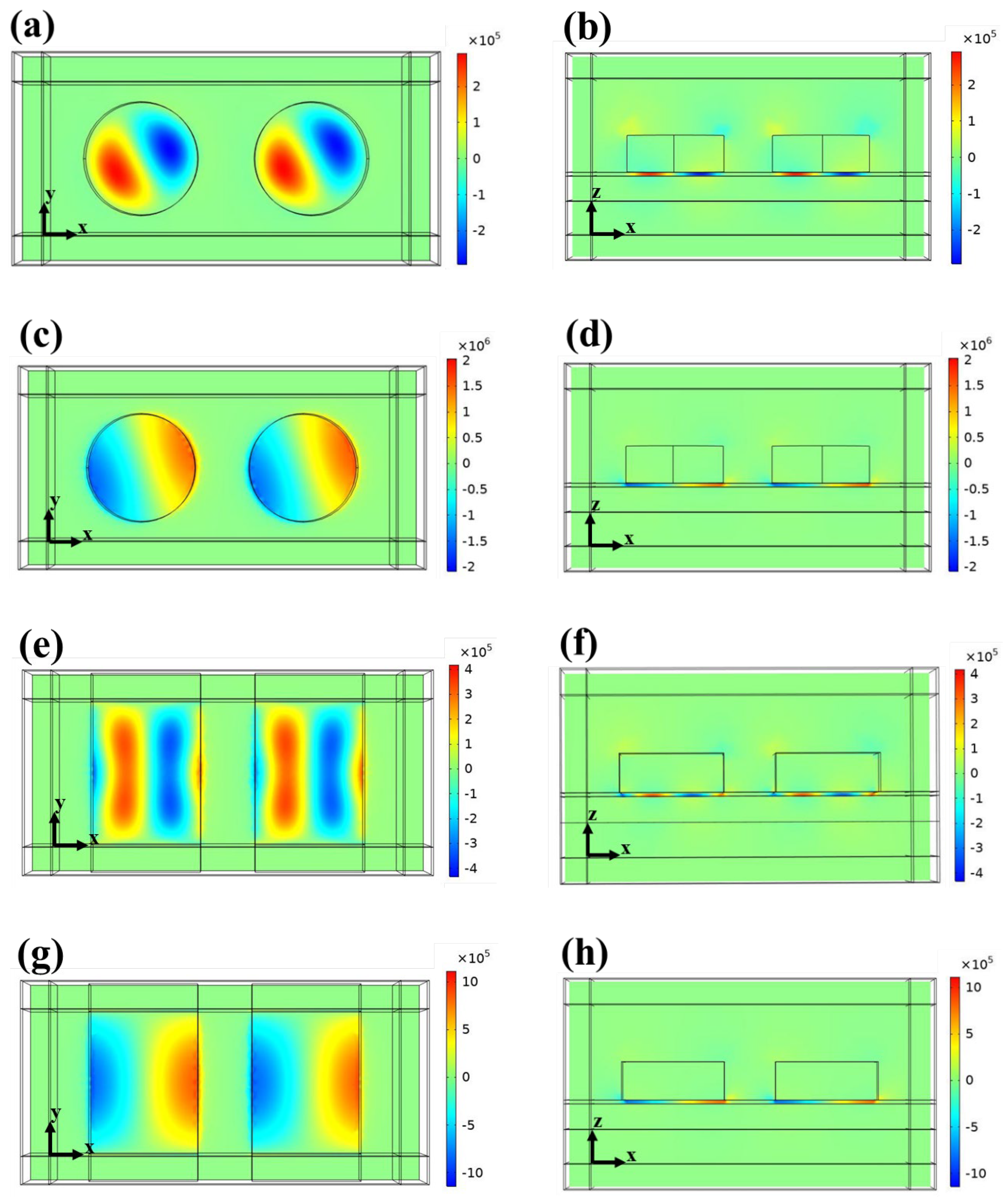
Figure 2, two different modes were observed in spectrum for each structure. However, based on this figure can not explain the reason for the emergence of mode I, Therefore, the z-component of the electric field profile distribution was calculated for both structures and shown in
Figure 4a–h.
Figure 4a,b show the mode I of the structure with nanodisk array at a wavelength of 720 nm from different views of the xy and xz planes, respectively. The Z component of the electric field on this structure shows that mode I could be a combination of a dipole (bright mode) and a plasmonic radial breathing dark mode. The plasmonic radial breathing dark mode, which is characterized by a radially oscillating charge density, arises from the surface plasmon waves trapped in the flat nanoparticles [
27,
32,
33]. This mode does not couple to light and will escape observation in optical experiments. This radially breathing mode has the character of an extended two-dimensional surface plasmon with a wavenumber determined by the circular disk confinement. In this mode, the distribution of the electric field shows a ‘hotspot’ pattern with the highest intensity in the center of the edges of the nanodisks.
The stronger mode at 1250 nm in
Figure 4c,d shows a stronger z-component of the electric field, as expected from
Figure 3. At this wavelength, a uniform field distribution is obtained around the edges of the nanodisks. This uniformity is indicative of a dipolar plasmonic resonance, which is common for spherical or circular structures such as nanodisks. The edges show a stronger field due to the curvature of the disks, which concentrates the electric field.
Figure 4e,f shows the z-component of the electric field distribution for mode I for the structure with nanostrip array. As can be seen from the literature [
27,
34], this mode is probably related to the higher order plasmonic modes. As the electric field in
Figure 4e,f shows, it is more distributed along the surface between the nanostrips compared to mode II in
Figure 4g,h. This difference indicates a different mode of plasmonic resonance affecting a larger area of the surface. The localized enhancement along the edges of the nanostrips is still visible, but appears to be less intense than for mode II. Similar to the x-y plane for mode I, the electric field is present at the edges, but not as intense as for mode II. The field appears to be more uniformly distributed along the height of the nanostrips, indicating a different interaction of the plasmonic mode with the incident light at this wavelength.
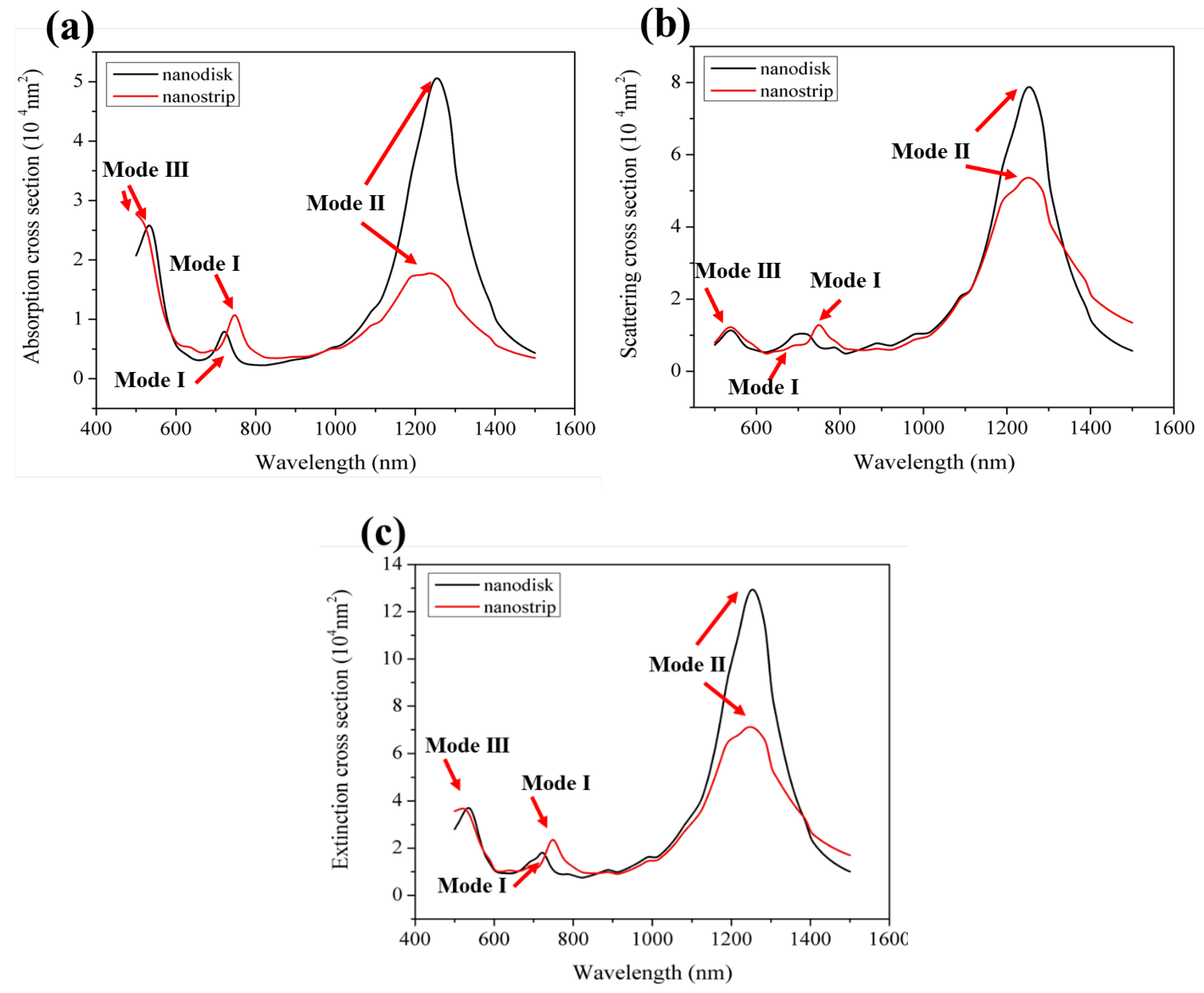
In
Figure 5 three diagrams show the absorption, scattering and extinction cross sections as a function of wavelength for two different plasmonic structures proposed in this work.
Figure 5a shows how much light is absorbed by the plasmonic structures at each wavelength. As it can be seen, the black diagram belongs to the nanodisk array and for this structure there is a dominant absorption peak at 1250 nm (mode II), which belongs to the dipole mode as explained above. As expected, a weaker peak is observed at 720 nm (Mode I). However, another peak (mode III) was also obtained at shorter wavelengths for both structures (535 nm for the nanodisk and 510 nm for the nanostrip structure), which was not observed in
Figure 2. To explain this mode, the normalized electric field distribution is derived and shown in
Figure 6a,b for nanodisk and nanostrip arrays, respectively. As can be seen in these two figures, the LSPR arises in the corners of the nanodisks and nanoarrays in air instead of the gap layer. This is the reason for the absence of the peak at these wavelengths in
Figure 2. Similarly, the red plot shows the absorption response of the nanostrip structure. As expected, two strong (Mode II) and weak (Mode I) resonant modes as well as Mode III were observed in this case. The peaks of modes I and II are probably due to the excitation of different plasmonic modes in the gap layer, which is facilitated by the elongated shape of the nanostrip.
The comparison of the strong modes of the two structures shows that the nanodisk array has a stronger absorption at its mode II. This difference shows that each structure has different resonance properties and that their absorption efficiency varies with wavelength. The choice between nanodisk and nanostrip in the application would depend on the specific wavelength at which the device is intended to operate.
The variation of scattering cross-section with wavelength in
Figure 5b shows how much light is scattered by the plasmonic structure at each wavelength. Similar to the absorption cross section, three peaks are observed for each structure. In agreement with the strong absorption at 1250 nm for both structures, high absorption often correlates with high scattering at the resonance frequency. The higher magnitude of the scattering peaks for the nanodisk compared to the nanostrip at these wavelengths suggests that the nanodisk may be more effective in applications where scattering is desired, such as in optical sensing or as scattering centers in photonic crystals. The observed differences in absorption and scattering between the nanodisk and the nanostrip can be attributed to their different shapes and sizes, which affect the electric field distribution around them and the plasmonic resonance conditions.
The resonant peaks in both the absorption and scattering cross sections are important for the design of plasmonic devices, such as sensors, where the choice of structure depends on the operating wavelength to maximise efficiency.
Based on Equation (4), the extinction cross-section is a measure of the total power loss of the incident light due to absorption and scattering by the plasmonic structure. It can be uniquely determined by adding the magnitudes of the absorption and scattering cross sections at each wavelength in
Figure 5a,b and comparing the result with the measured extinction cross section magnitude in
Figure 5c at the same wavelength. These calculations at resonant modes were performed for both structures and are shown in Table 1.
Such diagrams, as shown in the plasmonic context in
Figure 5, are crucial for understanding how different shapes and sizes of nanostructures interact with light. This information is important for the development of plasmonic devices for applications in areas such as photothermal therapies, optical filters and sensors. The peaks in the extinction cross-section correspond to wavelengths at which the nanostructures may be particularly effective in applications that require amplification of electromagnetic fields, such as surface-enhanced Raman scattering (SERS) or photodetectors.
| |
Nano-disk
(mode I)
nm2
|
Nano-disk
(mode II)
nm2
|
Nano-disk
(mode III)
nm2
|
Nano-strip
(mode I)
nm2
|
Nano-strip
(mode II)
nm2
|
Nano-strip
(mode III)
nm2
|
| Absorption cross section |
0.82×10⁴ |
5.1×10⁴ |
2.56×10⁴ |
1.12×10⁴ |
1.65×10⁴ |
2.75×10⁴ |
| Scattering cross section |
1.05×10⁴ |
7.85×10⁴ |
0.82×10⁴ |
1.33×10⁴ |
5.45×10⁴ |
0.86×10⁴ |
| Extinction cross section |
1.89×10⁴ |
13.1×10⁴ |
3.45×10⁴ |
2.41×10⁴ |
7.1×10⁴ |
3.65×10⁴ |
In sum, the comparative simulation of plasmonic nanostructures, especially periodic metal nanostrip and nanodisk arrays on a mirror separated by an ultrathin Al2O3 layer, shows different optical responses. The electric field enhancement factor illustrates two resonance modes, with mode II, representing the dipolar plasmonic resonance, showing a significantly stronger field enhancement for the nanodisk array at 1260 nm compared to the nanostrip array at 1250 nm. The z-component analysis of the electric field distribution highlights the nature of these modes and emphasizes the efficiency of the nanodisks in interacting with incident light. In addition, the absorption, scattering and extinction cross sections show different resonance peaks for the two structures, highlighting their application-specific efficiency. The nanodisk array, with its stronger absorption and scattering at the dipole resonance wavelength, offers improved performance in applications such as surface-enhanced Raman scattering and photodetectors. This comprehensive understanding of plasmonic behavior helps in tailoring nanostructures for optimal performance in various applications and advances the development of plasmonic devices for various technological fields.
