1. Introduction
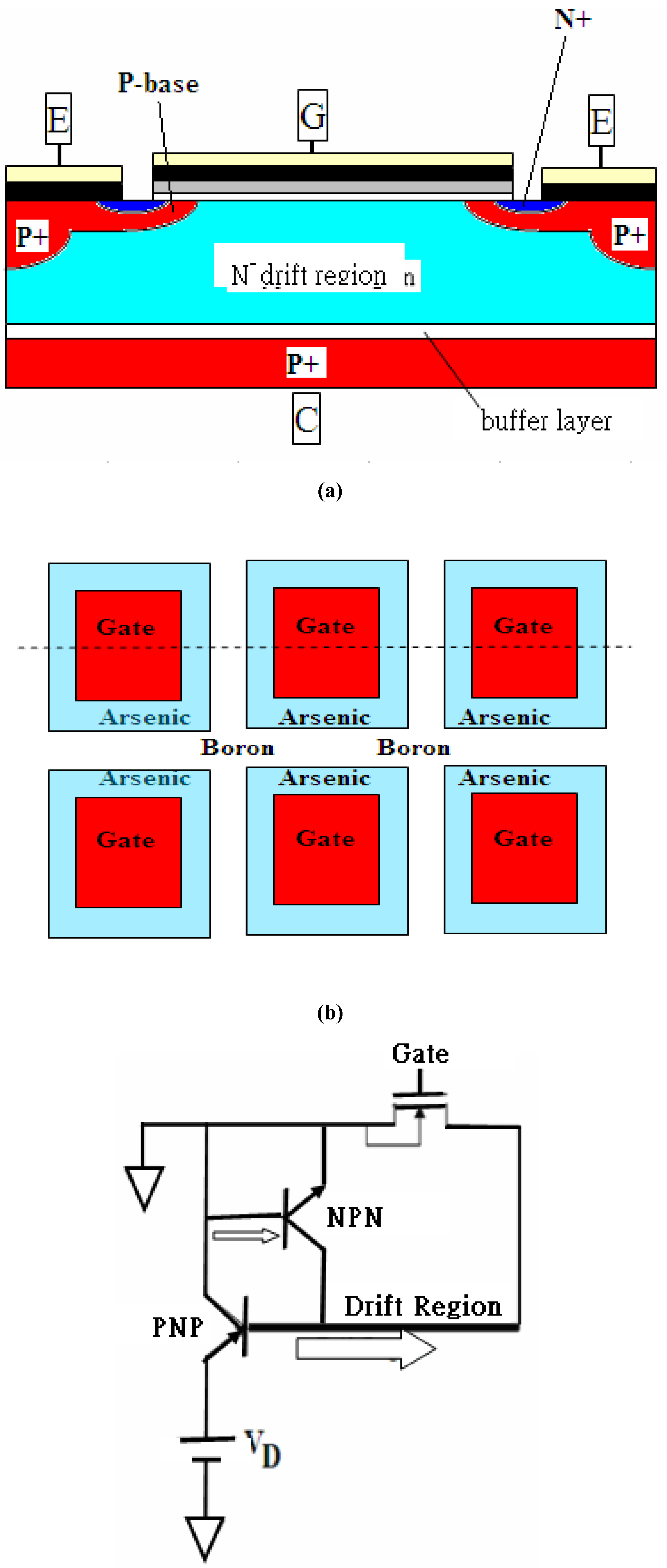
Power discrete transistors with high breakdown voltage require low on-resistance, and Isolated Gate Bipolar Transistor (IGBT) belongs to one of them. IGBT refers to the isolated gates of Metal-Oxide-Silicon Field Effect Transistor (MOSFET) with high input impedance and Bipolar Junction Transistor (BJT) with high current gain. On one hand, there exist insolated gates, beneath which double diffusions of Arsenic and Boron simultaneously undertake at high temperature to form N channel MOSFET. Such NMOSFET structure appears duplicating the traditional power MOSFET. IGBT is specially unique at Emitter or Source, where an extra heavily doped Boron in the central parts surrounded by heavily doped Arsenic nearby Gates as shown in
Figure 1a-b. An equivalent circuit in
Figure 1c may address the cross section of IGBT. On the second hand, the current contributed and controlled by MOSFET triggers BJT in the equivalent circuit, which turns on by the applied bias on the Gates. There are two types of BJT, NPN and PNP. The P-type semiconductor in the middle of NPN is the triggering Base and the other two N-type ones are Emitter/Collector, while The N-type semiconductor in the middle of PNP forms triggering Base and the other two P-types signify Emitter/Collector. I
CE current of BJT is associated with Base current by either inputting or extracting current, and enjoys high current gain in many applications.
From the whole picture point of view, the drift current flowing from bottom to top confronts the resistive drifting region due to the low N-type dose concentration on the paths. Even so, low dose concentration means low possibility of avalanches, which is thus associated with higher sustainable breakdown voltage like other power discrete devices. Therefore, IGBT is worth watching both because of its high breakdown voltage and because of, especially, the internally equivalent BJTs contributing high current gain (both from NPN-BJT and PNP-BJT) with insulated-gate controlled Base current triggering. IGBT is thus able to achieve high power controllability. Nevertheless, the current drifting through drifting regions may generate Ohmic heat, which could further become distinguishable interferences to the soaring current as the applied Drain-Source (V
DS) or Collector-Emitter (V
CE) bias increases. The characteristic current curves receive down graded factors and need modifying. Electrical performances may thus show degraded as the unwanted heat appears, which is intriguing and exploring. In addition, there somehow seems to be another concern, parasitic Thyristor. The mechanism demonstrates in
Figure 1c, which addresses the mutual triggering fact that receives no control from the gate. Fortunately, the top Emitter and Source are heavily doped boron and arsenic, which may provide conducting charge bank and protect the equivalent parasitic Thyristers from activating or triggering that would cause latching up.
Since the impressive controllability make IGBT widely popular to the applications of physical models, among which numerical model actually provides physical depletion region modulation in the base region where carriers under ambipolar diffusion mechanism thus contribute transient collector currents. Diffusion mechanism applies to Diode, and two back-to-back Diodes form a Bipolar. Using numerical model has the precise prediction on carrier performances but requires professional manipulation on the dose concentration settings. A model was proposed to take into account the dynamic behaviors of carriers which are injected into equivalent Base. The circuit simulator, SABER, then generates the answer. ATLAS 2-D numerical simulator was introduced to first evaluate the electro-thermal performances that are helpful to predict IGBT destruction phases. In order to predict the power loss and electro-magnetic interference (EMI) noise, capacitance change is focused during switching operation. The power loss and EMI noise are again predicted by free-wheeling diode model, which considers bipolar carrier dynamics to reproduce the measured turn-on switching waveform for multiple external gate resistance. The second generation IGBT model uses high voltage MOSFET to dynamically vary the equivalent resistance of BJT. Basically, numerical simulator (ATLAS) uses BJT-associated parameters addressing the internal equivalent circuit to fit the experimental curves. Resistance mainly contributes thermal irrigation causing trouble to carrier flow. Somehow, the whole drift region suggests that statistical ways of thermally treating power discrete may be a good way to fit the characteristic curve. In a field stop trench-gate IGBT model, parameters are elaborately extracted to successfully match the experiment result. But the manufacturing defects like voids are always very concerning because non-controllable number and locations of voids in fabrication are truly challenging. For vertical power discrete, physical stresses and strains due to assembly and thermal cycle correlate with electrical performances of IGBT. Finite element model proposes a feasible mesh (smaller elements from a large system) to solve the differential equation addressing IGBT on non-punch-through IGBT. The electromagnetic potential profile may be numerically analyzed. The extraction of parameters is successful but tedious for fitting. In addition to non-punch-through (NPT) IGBT, punch through (PT) IGBT mainly performs uniquely by introducing a buffer layer with N+. With the merits of NPT and PT IGBT, field-stop IGBT also introduces a buffer layer without dosage [
1,
2,
3,
4,
5,
6,
7,
8,
9,
10]. Nevertheless, most provided models mainly looks to BJT activated by imposing carriers into Base of it. Excellent work of simulation on computer does help a lot.
On the other hand, another concise model at the wafer level in this study is worth posing. First of all, the bottom-top current, I
CE, flows as bottom-top bias, V
C, applies to IGBT discrete device. Due to the development of certain fitting skills [
11,
12], many results are so inspiring and conclusive, including nanometer-scale process limit, the thickness of strong inversion layer, and threshold voltage size-associated trend. In the sense, IGBT characteristic curves are worth fitting by using a brand-new modified formula with three parameters, i.e., the size and mobility related k
eff, threshold voltage related V
th, and Early Voltage related λ as presented in Equation (1) and (2). The term addressing uncertain phonon disturbance or kink effects is concerning. Therefore, well fitting the electrical characteristic curves helps understand possible underlying mechanism.
In the paper, preparation and measurement in section 2 are mentioned following the introduction. In section 3, a new algorithm for equations is to fit the characteristic curves. In section 4, kink effects addressing generated heat help well fit the curves, and terminal speeds of carriers explain the saturated curves in saturation region. So there come the conclusions in section 5.
2. Preparation and Measurements
Silane (SiH
4) flows over the heavily boron doped silicon substrate at low pressure with the help of hydrogen chloride to grow 3nm pure flawless epi-silicon, which is called “buffer layer” without any adulterant. After the growth of buffer layer, SiH
4 is kept flowing with phosphorus doped in the mean time of growing. This n-type epitaxial silicon is then processed at high temperature in oxygen ambient to grow thick silicon dioxide followed by guard ring photo mask for defining guard ring trench area, wet oxide etching, and guard ring boron implant. Guard ring trenches and boron implant may adjust the field distribution as the voltage is applied. Active area photo mask and the following wet etching again define the active area where carriers move around. The epi-silicon in the defined active area now exposes to the air such that dry silicon dioxide grows onto the silicon surface in the dry oxygen ambient at high temperature to form gate oxide. There come the heavily doped poly-silicon, poly-silicon gate photo mask, and gate poly-silicon etching with end-point detector to define insulated gate location, followed by consecutive boron photo mask, boron implants, arsenic photo mask and arsenic implants. Required is double-diffusion at high temperature, which activates already-implanted boron and arsenic and accurately define where the channels are located. The collectors and emitters appear in
Figure 1, which also demonstrates the cross section, the corresponding layout overlook, and the equivalent circuit. The following metal-1 shorts all the concerning gates and defines the test areas. The metal-2 layer completes the pads for probe locations.
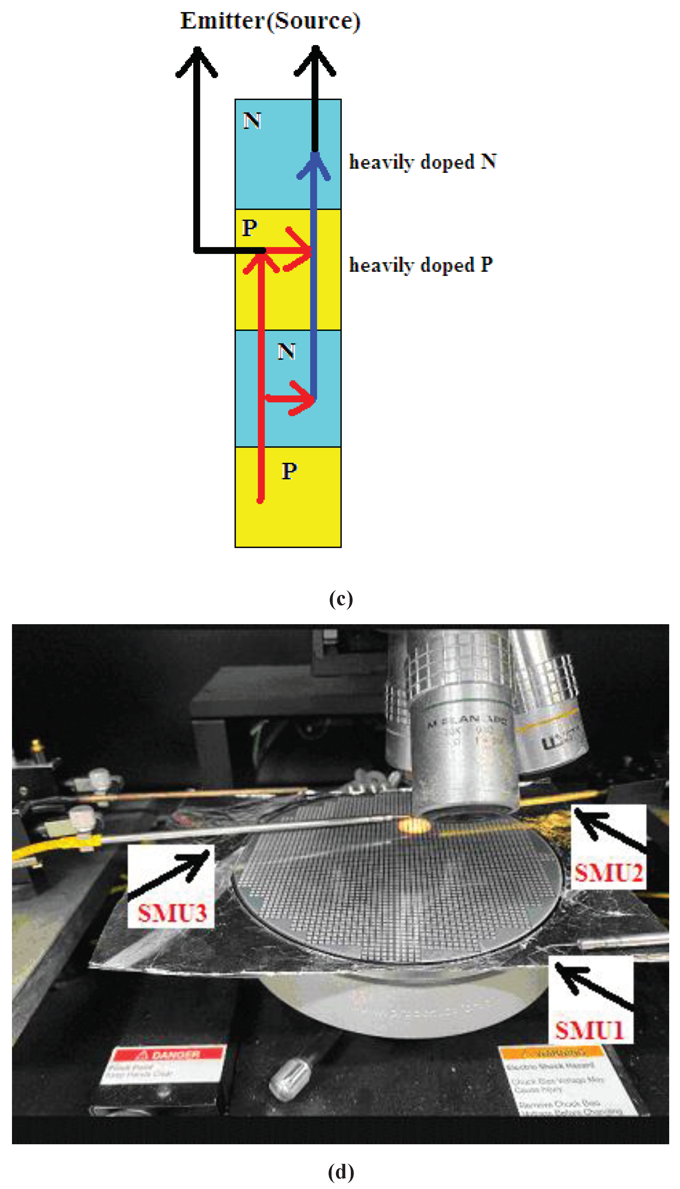
The fabricated IGBT is loaded to Agilent 4156C probe station with an applied bias, VC, to the bottom (SMU1), which attaches to aluminum foil with the help of silver glue and the top emitter pad. Even though the power is required to be large enough, the current compliance is set to 100mA, which is the maximum current for the probe to the ground (SMU2 for receiving measurable current) to protect the probes from fast consuming. The threshold voltage is the minimum applied voltage to the insulated gate so that non-zero IC can be measured. Since the linear threshold voltage is found to be 4.2V at VD = 0.1V, the starting gate bias (SMU3) on the insulated gate is set to 4.3V, followed by VG=4.4, 4.5, 4.6, 4.7, and 4.8V. IC at VG≧4.9V is not presented because the current is already over 100mA for IC is already 50mA
3. Results and New Algorithm
I
C-V
C characteristic curves at V
G=4.2, 4.3, 4.4, 4.5, 4.6, 4.7, and 4.8V appear like BJT as shown in
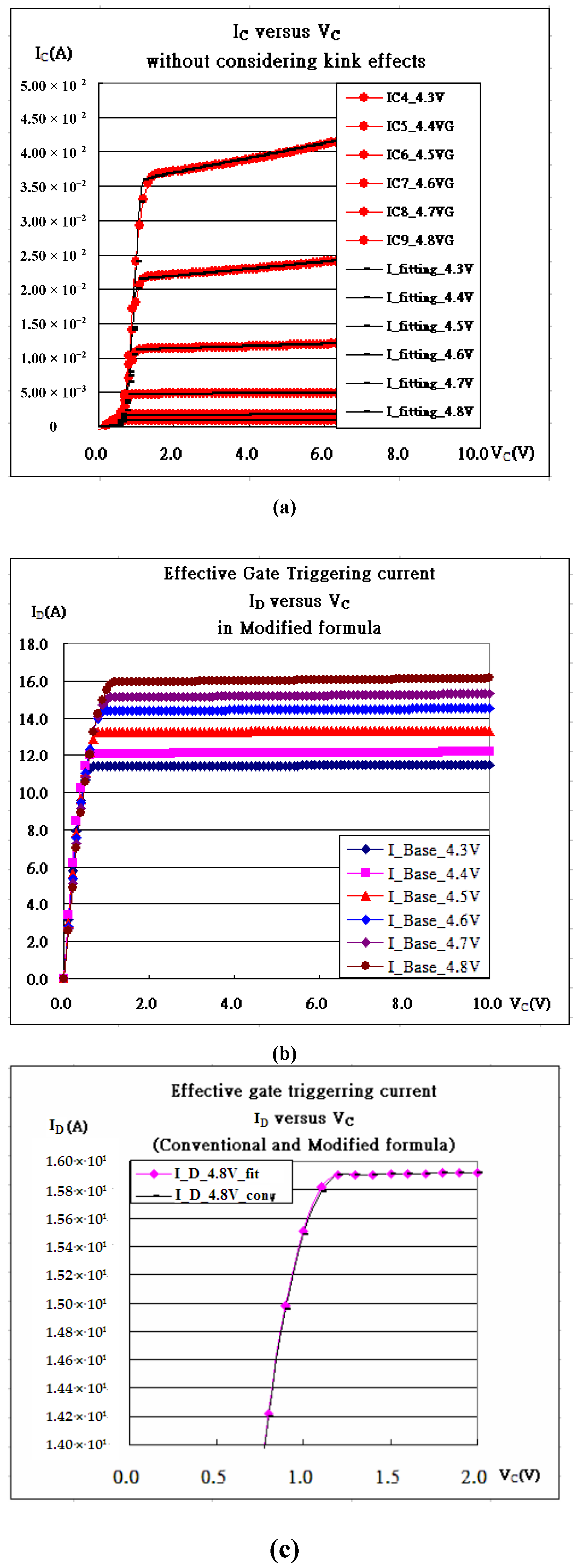
Figure 2a, which, in a sense, may be characterized as two back-to-back connected diodes. The whole mechanism includes two regimes at certain V
B: (A) The first one is dominantly expressed as a modified diode model, which is exponentially soaring as V
C bias is initially increased. This regime may cooperate with triode region in Equation (1) and (2) (triode region). (B) The second one is mainly concerning suppressing effects coming from the reverse bias of the diode, and I
C thus gets saturated. This regime may cooperate with the saturation region in Equation (1) and (2) (saturation region). [
13] The above (A) and (B) bring the idea that IGBT is addressed by the modified Ebers-Moll Model containing Shockley equation as stated in Equation (1), which is activated by MOSFET as described in Equation (2). Both equations in the above empirically characterize the measured electrical curves, and the chosen parameters successfully fit the curves (the curves in black as shown in
Figure 2a, which is encouraging.
Explicitly, the formula Equation (1) for I
C makes sense as I
D in Equation (2) triggers BJT while I
DS is intrinsically taken control of by V
G according to the conventional formula depending on whether V
C is less then
(VG-Vth) or V
C is larger than
(VG-Vth). Nevertheless, the modified parenthesis
(1+λVD) in Triode regime in Equation (2) does make only a little different in
Figure 2b and 2c since the
λ is nearly equal to zero; the triggering fitting characteristic curves of effective MOSFET in saturation regime are almost flat. [
14]
and
Where I
o is defined to be a current scale constant, α
ο(1/A) is a effective constant making (α
οI
DS) dimensionless, λ is inversely proportional to absolute value of effective Early Voltage, and k
eff (A/V
2) is set to be linearly proportional to the effective mobility, and associated with sizes of isolated gates. The parameters, (k
eff, V
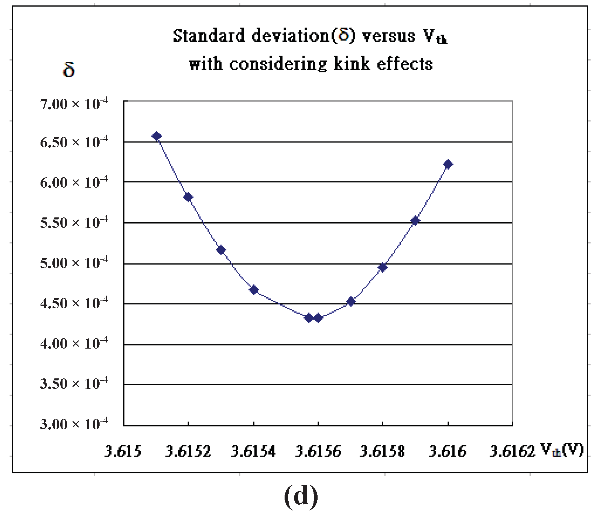
th, λ), are always determined to minimize the following deviation (δ) in Eq.(3) such as
Figure 2d:
4. Discussion and Analysis
The new algorithm for IGBT might provide theoretical insights to understand how it works. Somehow, apparently found are discrepancies at various gate bias in
Figure 2a, which are unsatisfactory. Referring to the kinks proposed in [14], electrons and holes travel through the periodic diamond structure and posses the potential energy density
V(φe)=(a/b)[1-cos(bφe)], where
V(φ
e) is thought to be non-negative. Also, carriers like electrons and holes are fermions, which are expressed by wave function as

with
ϋf obeying Fermi-Dirac statistics while the moving fermion scalar field,
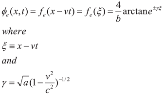
φe, refers to the nonlinear sine-Gordon equation [15] as follows:
What a coincidence that the nonlinear solution
y = arctan[exp(t/2)] versus
t does look like I
D-V
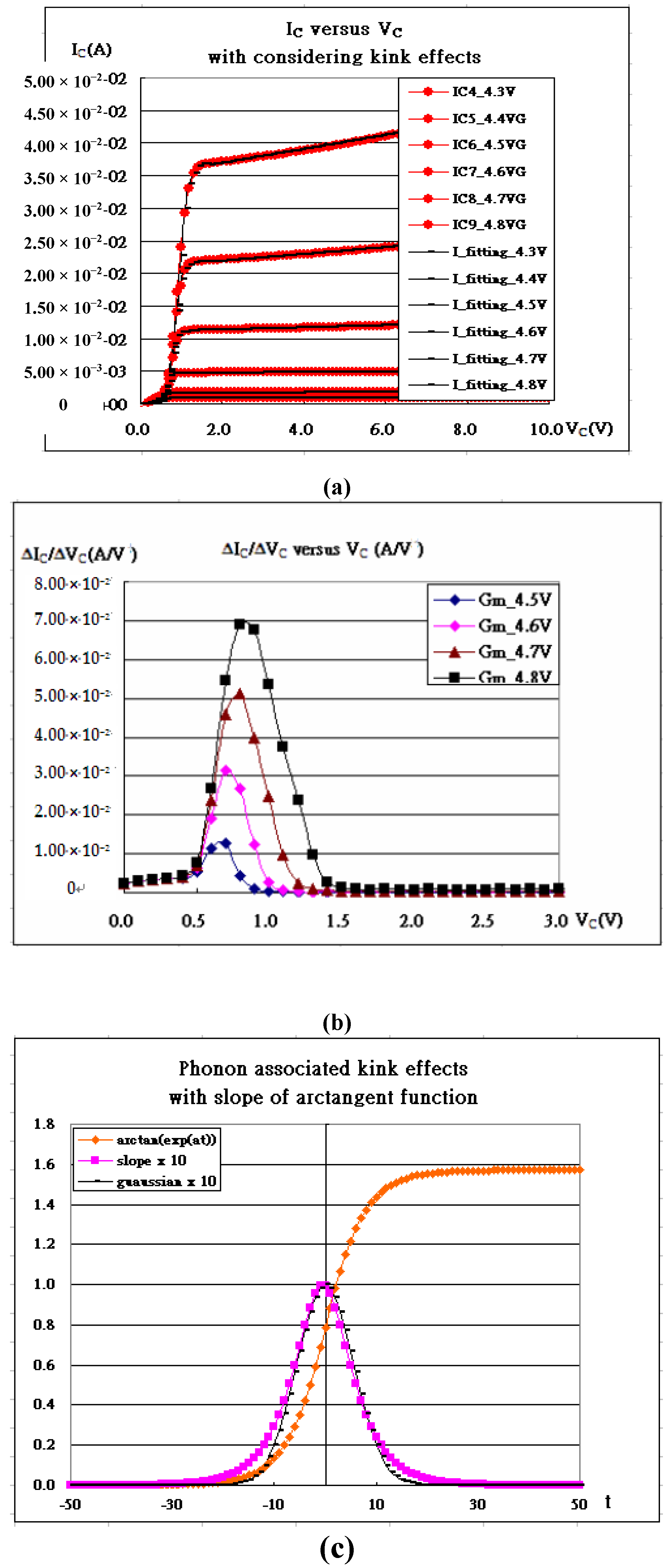
D characteristic curves of IGBT. Its Gaussian-like first derivative in Equation (7) causes heat dissipation problems, which result in extra heat and thus the speed variations of carriers, which correspond to Gaussian-like current correction, such as Bremsstrahlung radiations and synchrotron radiations. After considering kink effects, there show
Figure 3a with
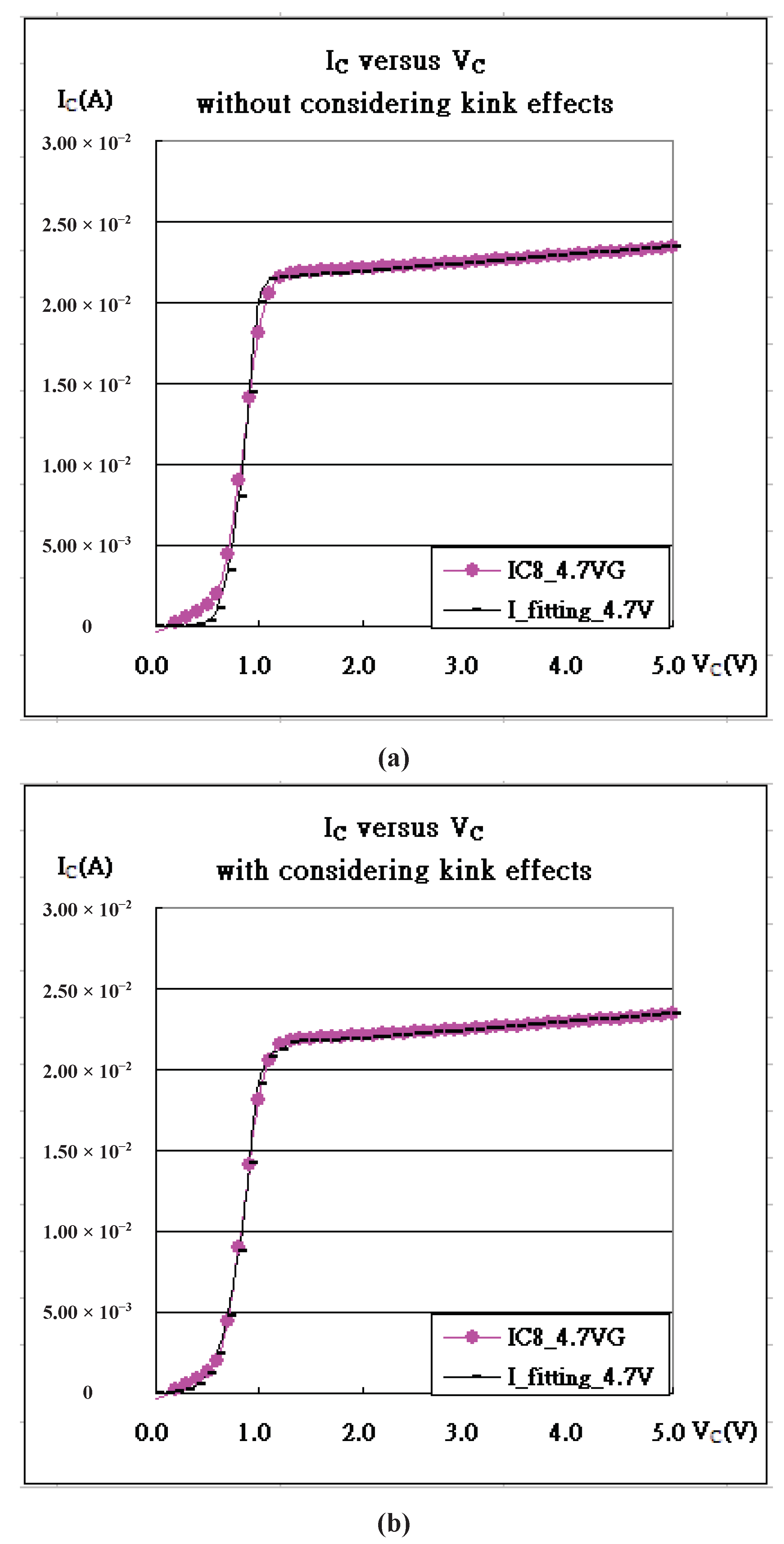
Figure 3b,3c. The magnified pictures refer to
Figure 4a with
Figure 4b at V
G=4.7V and
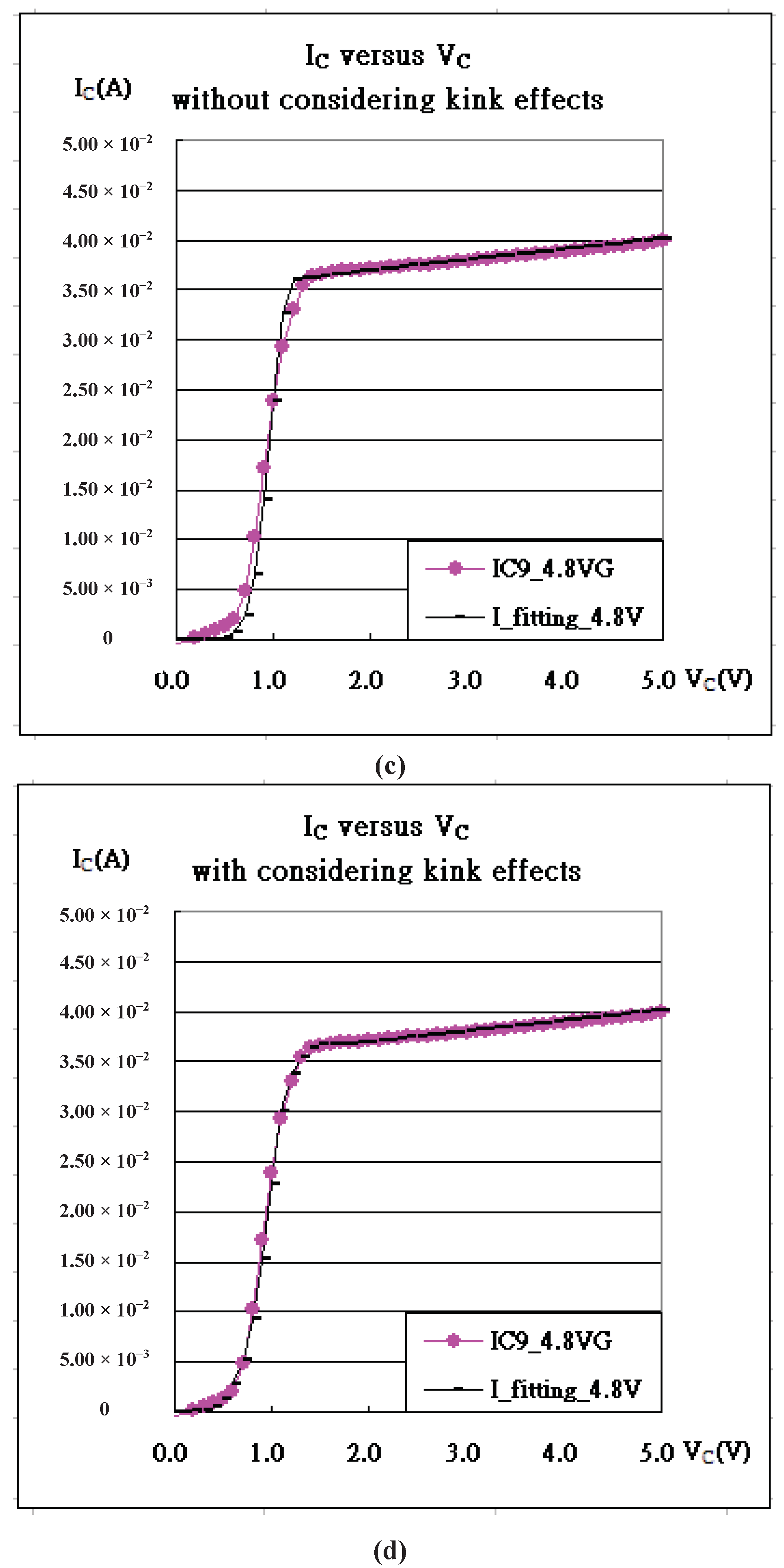
Figure 4c with
Figure 4d at V
G=4.8V. The extra modified equation refers to Equation (8) as follows:
where the parameters, (α, β, χ), are added to address bulk phonon effective coefficients, V
D corresponds to V
C, and I
C corresponds to I
C in this paper. The determined parameters refer to
Table 1. As α
ok
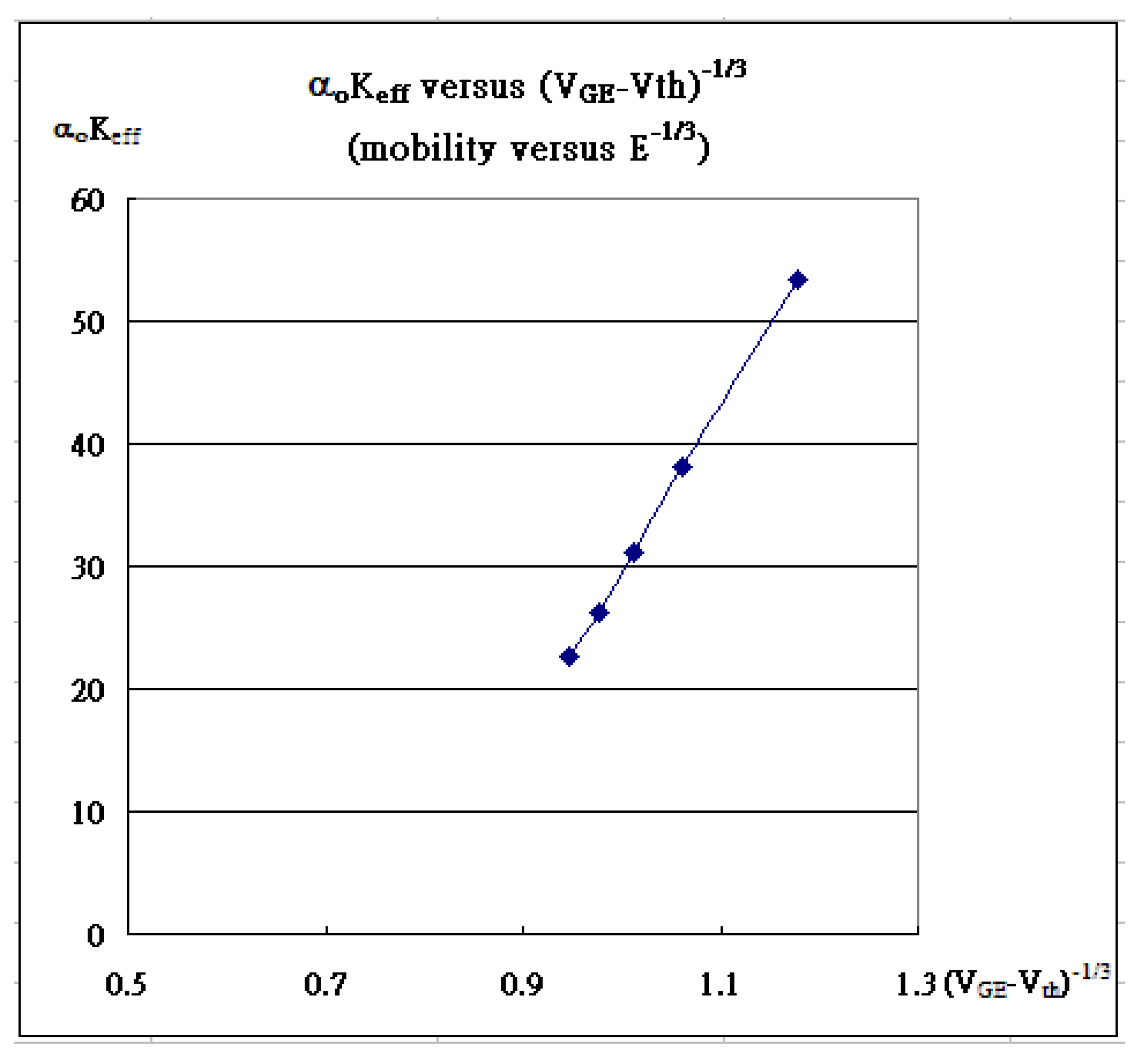
eff (Dimensionless) versus (V
G-V
th)
-1/3 is taken into account, it is equivalent to mobility versus E
-1/3. Even though both are not proportional to each other, mobility is linearly dependent of E
-1/3. Note that the first pair (53.4325, 0.60867
-1/3) is the average of V
G=4.3V and 4.4V because both curves are quite close
Furthermore, current flows because of flowing carriers, moving electrons or holes, which carry electrical power or signals. Somehow, the current, I
C, eventually gets saturated and reaches a certain quantity since the carriers can not be accelerated any more and stay at a maximum speed. The electrical force accelerates carriers and cancels with the frictional force, which is proportional to the Nth power of the speed and opposite to the moving direction of carriers. For simplicity, only electrons are taken into account and the total force F is characterized as follows:
where α is a viscosity coefficient, m is the mass of carriers, and E is the electrical force coming from the applied bias across the channel. Before electrons reach the maximum speed,
where
l is the traverse distance length that the electron travels as
E is applied. So,
From Equation (7), the traverse distance
l may approach to infinity as the speed approaches to certain value at certain applied electrical field
ED =VDS/L as stated below:
and
which gives the information that the mobility in the conventional
ID(VD, VG) formula in Equation (2) is constant only when
N=1 at certain fixed gate bios. And the mobility (μ) is then expressed as follows:
which verifies the constant mobility at certain fixed gate bios referring to a fixed electrical field EDS that is proportional to (VG-Vth).
In summary, there are indeed three specific groups of parameters and constants: Group 1 includes Io, keff, and αο as in Equation (1) and Equation (2), where αο is used to make (αο ID) dimensionless. Group 2 includes (α, β, χ) as in Equation (3). Group 3 includes α’. which is a viscosity coefficient as in Equation (4). Some still need more study to identify in the near future.
5. Conclusion
In this paper, several parameters are thus determined to fit electrical characteristic curves. Those extracted parameters are useful to help understand the basic underlying physics. The fitting algorithm and the fitting deviation do impressively explore IGBT. First of all, the threshold voltages at various VG’ are commonly determined to be 3.6V, which is different from the one determined in ID-VG and λ = 0.001 (1/V). αοkeff varies from 55.7 to 22.6 (1/V2) at (VG-Vth) = 0.6087V, 0.8331V, 0.9621V, 1.0731V, and 1.1844V, and implies that mobility decreases as the electrical field gets stronger because of stronger field attracting carriers toward the gate dielectric and causing glue-sticking effects.
The fitting in
Figure 4 with α≠0 definitely prove that I
C gets disturbed and suppressed because of speeding generated heat that happens as carriers go through the crystal. The abruptly generated heat hits the summit and is hard to conduct in time. The hesitated heat therefore causes trouble and reduces I
CE as seen. In another words, the mobility degraded unexpectedly.
Finding a promising way to fit the measured data is intriguing. Neither BJT nor MOSFET can independently explain the characteristics of IGBT. Due to the surprisingly well fitting, the two added mechanisms with α≠0, may play significant roles to propose reliable processes, such as the assessments of buffer layers or dose concentrations in drifting region. Somehow, the deviations among the soaring data in the rising curves are not perfect as appeared in
Figure 4b and 4d. Hopefully, more can be done in the near future.
Furthermore, as VD/VC increases, the current soaring saturation is mentioned even in the conventional formula in Equation (2). Just like rain fall, Equation (4) addresses the mechanism by using something like frictional term, which is proportional to the speed to the Nth. In semiconductor, the speed of carriers is apparently related to mobility, which is often taken to be constant. The mobility is found to be constant only if N is set to 1 as described in Equation (9).
Therefore, current proposed kink effects successfully provide quantities-characterization. Wishfully, the kink algorithm might be a good initiation for generating satisfactory ways somehow to understand the implicit underlying physics.
Author Contributions
Conceptualization, H.C. Yang, S.C. Chi, P.J. Yang, and B.H. Huang; methodology, H.C. Yang. and S.C. Chi.; software, H.C. Yang. and S.C. Chi; validation, H.C. Yang. and S.C. Chi.; formal analysis, H.C. Yang. and S.C. Chi.; investigation, H.C. Yang. and S.C. Chi; resources, H.C. Yang. and S.C. Chi; data curation, H.C. Yang. and S.C. Chi;.
Institutional Review Board Statement
Not available.
Informed Consent Statement
Not available.
Data Availability Statement
No.
Acknowledgement
All the authors sincerely thank Patrick for his supporting this project.
Conflicts of Interest
No.
References
- Hefner, A.R., Jr.; 1988 IEEE Industry Applications Society Annual Meeting, 1988, Page(s): 606 - 614 vol.1.
- R. Kraus; K. Hoffmann; Proceedings of the 5th International Symposium on Power Semiconductor Devices and ICs, 1993 , Page(s): 30-34.
- Ammous, A.; Ammous, K.; Morel, H.; Allard, B.; Bergogne, D.; Sellami, F.; Chante, J.P.; IEEE Transactions on Power Electronics, Vol 15 , Issue: 4 Page(s): 778 – 790.
- Takeshi Mizoguchi; Yoko Sakiyama; Naoto Tsukamoto; Wataru Saito, 2019 31st International Symposium on Power Semiconductor Devices and ICs (ISPSD).
- Takeshi Mizoguchi; Yoshiko Ikeda; Naoto Tsukamoto, 2020 32nd International Symposium on Power Semiconductor Devices and ICs (ISPSD).
- Tone; Y. Miyaoku; M. Miura-Mattausch; H. Kikuchihara; U. Feldmann; T. Saito; T. Mizoguchi; T. Yamamoto; H. J. Mattausch, IEEE Transactions on Electron Devices, 2019, Volume: 66, Issue: 8.
- ang, X. et al. Improved Parameterization Methodology for a Field-Stop Trench-Gate IGBT Physical Model by Switching Feature Partitioning. IEEE Journal of Emerging and Selected Topics in Power Electronics, vol. 11, no. 4, pp. 3983-3994, Aug. 2023. [CrossRef]
- Rodriguez, M. et al. Reconfigurable special test circuit of physics-based IGBT models parameter extraction. Solid-State Electron., vol. 54, no. 11, pp. 1246-1256, Nov. 2010. [CrossRef]
- Chibante R. et al., Finite-element modeling and optimization-based parameter extraction algorithm for NPT-IGBTs", IEEE Trans. Power Electron., vol. 24, no. 5, pp. 1417-1427, May 2009. [CrossRef]
- Yoshida, T.; Takahashi, T.; Suzuki, K.; Tarutani, M. The second-generation 600V RC-IGBT with optimized FWD. 2016 28th International Symposium on Power Semiconductor Devices and ICs (ISPSD), Prague, Czech Republic, 12-16 June 2016; pp. 159-162.
- Zhu, C. et al. A floating dummy trench gate IGBT (FDT-IGBT) for hybrid and electric vehicle (HEV/EV) applications. 19th European Conference on Power Electronics and Applications (EPE'17 ECCE Europe), Warsaw, Poland, 11-14 September 2017; pp. 1-7.
- Chen J., Ma, Y., and Yang, S., A numberical method for solving the physics-based model of IGBT with all free-carrier injection conditions in the base region. COMPEL The international journal for computation and mathematics in electrical and electronic engineering. Vol. 36 No.6, pp1653-1662.
- A Pirondi, G Nicoletto, P Cova, M Pasqualetti, M Portesine, Thermo-mechanical finite element analysis in press-packed IGBT design. volume 40, Issue 7, July 2000, Pages 1163-1172. [CrossRef]
- Yang, H.-C.; Chi, S.-C. Process Corresponding Implications Associated with a Conclusive Model-Fit Current-Voltage Characteristic Curves. Appl. Sci. 2022, 12, 46. [CrossRef]
- Yang, H.-C.; Chi, S.-C.; Liao W.S. Comparison of Fitting Current–Voltage Characteristics Curves of FinFET Transistors with Various Fixed Parameter. Appl. Sci. 2022, 12, 10519. [CrossRef]
- Zhang, F.; Yang, X.; Xue, W.; Xie, R.; Li, Y.; Sha, Y. A fast IGBT model considering the dynamic performance of both IGBT and antiparallel diode. IEEE Applied Power Electronics Conference and Exposition (APEC), San Antonio, TX, USA, 04-08 March 2018; pp. 276-279.
- Yang, H.-C.; Chi, S.-C. Conclusive Model-Fit Current-Voltage Characteristics Curves with Kink Effects Appl. Sci. 2023, 13, 12379. [CrossRef]
- Ryder, L. H. The sine-Gordon kink, In Quantum Field Theory, the Press Syndicate of the University of Cambridge, Cambridge , UK, 1985, pp402.
Figure 1.
(a) The simplified cross section of fabricated IGBT. (b)The simplified layout overlook with the detached line corresponding to the cross section in (a), and double diffusion (c)The equivalent current flow for IGBT discrete. (d) The probe station with aluminum foil attached to the back of the wafer, which the probe, named SMU1, is applied to as VC. SMU2 is applied to the Emitter as ground and detect the current. And SMU3 is applied to the VG controlling the Gate.
Figure 2.
(a) The characteristic curves, IC-VC, and their fitting of IGBT at VG=4.3, 4.4, 4.5, 4.6, 4.7, and 4.8V without taking the kink effects into account. (b)The triggering MOSFET characteristics curves. (c) Comparison between conventional triggering current and modified triggering current. (d) The best fitting current determined and addressed by Vth.
Figure 3.
(a)The characteristic curves, IC-VC, and their fitting of IGBT at VGE=4.3, 4.4, 4.5, 4.6, 4.7, and 4.8V with considering kink effects. (b) The characteristic curves,Gm(ΔIC/ΔVC) of IGBT at VGE=4.5, 4.6, 4.7, and 4.8V. (c) Non-linear solution looks like the characteristic curves of IGBT, and so does the first derivative of the solution looking like (b), which is to be Gaussian-like.
Figure 4.
The characteristic curves, ICE-VCE, and their fitting of IGBT (a) at VG= 4.7V without considering kink effects, and (b) at VG= 4.7V with considering kink effects, (c) at VG= 4.8V without considering kink effects, and (d) at VG= 4.8V with considering kink effects.
Figure 4.
The characteristic curves, ICE-VCE, and their fitting of IGBT (a) at VG= 4.7V without considering kink effects, and (b) at VG= 4.7V with considering kink effects, (c) at VG= 4.8V without considering kink effects, and (d) at VG= 4.8V with considering kink effects.
Figure 5.
αokeff (Dimensionless) versus (VG-Vth)-1/3 is equivalent to mobility versus E-1/3, in which the first pair (53.4325, 0.60867-1/3) is the average of VG=4.3V and 4.4V because both curves are quite close.
Figure 5.
αokeff (Dimensionless) versus (VG-Vth)-1/3 is equivalent to mobility versus E-1/3, in which the first pair (53.4325, 0.60867-1/3) is the average of VG=4.3V and 4.4V because both curves are quite close.
Table 1.
Determined parameters.
Table 1.
Determined parameters.
| |
VG=4.3V |
VG=4.4V |
VG=4.5V |
VG=4.6V |
VG=4.7V |
VG=4.8V |
| okeff (Dimensionless) |
51.142 |
55.723 |
38.2 |
31.06 |
26.195 |
22.625 |
| Vth (V) |
3.63257 |
3.74133 |
3.66687 |
3.63793 |
3.6269 |
3.61557 |
| V) |
0.00078 |
0.0008 |
0.0007 |
0.001006 |
0.00151 |
0.0017 |
|
0 |
0 |
0.00001 |
0.00008 |
0.001 |
0.0065 |
|
0 |
0 |
-15.0 |
-15.0 |
-15.0 |
-19.0 |
|
0 |
0 |
0.215 |
0.215 |
0.215 |
0.1 |
|
Disclaimer/Publisher’s Note: The statements, opinions and data contained in all publications are solely those of the individual author(s) and contributor(s) and not of MDPI and/or the editor(s). MDPI and/or the editor(s) disclaim responsibility for any injury to people or property resulting from any ideas, methods, instructions or products referred to in the content. |
© 2024 by the authors. Licensee MDPI, Basel, Switzerland. This article is an open access article distributed under the terms and conditions of the Creative Commons Attribution (CC BY) license (http://creativecommons.org/licenses/by/4.0/).


 with ϋf obeying Fermi-Dirac statistics while the moving fermion scalar field, φe, refers to the nonlinear sine-Gordon equation [15] as follows:

