Preprint
Article

Raman Analysis of Deposition Pressure Variations in Nanocomposite SiCN Coatings: A 4-Stage Model

Altmetrics

Downloads

150

Views

31

Comments

0

This version is not peer-reviewed

Submitted:

29 March 2024

Posted:

01 April 2024

You are already at the latest version

Alerts
Abstract
Polymer-derived ceramic (PDC) based coatings like Si-C-N and their derivatives are gaining importance day by day in N/MEMS and aerospace due to their thermos-mechanical stability and conductivity. The crystallized, amorphous, and near amorphous morphology of SiCN nanocomposite coatings based on deposition conditions requires thorough investigation for appropriate utilization as they lead to differences in mechanical properties (quantified using nanoindentation in this case). A 4-stage model was proposed based on Raman spectroscopy due to the N2-Ar pressure variations during the deposition process of SiCN coatings by magnetron sputtering. The integral intensity of the G (graphitic), disorder (D), and tetrahedral (T) peaks namely IG, ID, and IT were calculated after the deconvolution of the spectra. The sp2 domain size and defect parameters were evaluated and correlated with the hardness and different bond formation involving Si, C, and N. Image analysis revealed the atomic migration involved during the growth process leading to crystallization along with the formation of voids and defects. The observations were supported by FTIR and TEM-SAED analysis. The outcomes provide a foundation causing an urge to develop similar models with further elemental additions and correlate with various physical properties.
Keywords: 
Subject: Engineering  -   Metallurgy and Metallurgical Engineering

1. Introduction

The ternary nanocomposite material Si-C-N was first introduced to the scientific community as a high-temperature oxidation-resistant polymer-derived ceramic (PDC) [1]. PDCs combine the functional properties of polymers with the mechanical and chemical durability of ceramics. Polymer-derived ceramics (PDCs) have a polymer-like nanostructure and ceramic-like properties, e.g., creep and oxidation resistance [2]. Apart from high-temperature oxidation resistance, the hardness, as well as the high-temperature stability of the Si–N–C phase, exceeds those of SiC and Si3N4. The electronic band gap of 2.5–3.8 eV allows us to consider this material as a wide band gap and dielectric material. More importantly, the stability of β-C3N4 with comparable diamond hardness has been achieved in ternary silicon carbonitride. The Si-C-N phase diagram is shown in Figure 1a. The incorporation of Si in the CN deposit promotes the inclusion of nitrogen and leads to C3N4. There is also an excess of carbon in Si-C-N which manifests itself in different hybridization and crystallographic patterns based on the deposition condition adopted (Figure 1b).
The Si-C-N has shown stability up to 1600 °C and it remains in the amorphous state up to 1500 °C. These properties make silicon carbonitride a promising material for prospective applications such as structural ceramics, MEMS, hard protective coatings, and electronic materials [3]. SiCN is being currently looked for the absorption of electromagnetic waves (shielding) [4,5,6,7], as thin film pressure and temperature sensors [8,9,10,11], as a bonding layer for memory devices [12] MEMS magnetic devices [13] and even in endodontics [14]. Theoretical studies have shown SiC2N2 tetrahedra to be the most stable structure of SiCN. The SiCN was found to have very high hardness and abrasion resistance and was also found to be compatible with stainless steel. It has also been reported to show both metallic and piezoelectric properties and is a good alternative to SiC which only has insulating properties [15,16,17,18,19]. There have been several investigations on PDC coatings and derivatives of Si-C-N over recent years some of which are given in Table 1.
The electrical conductivity, electron flow, and even piezoelectricity found in Si-C-N, have led to their application in the manufacture of sensors and nano/micro-electro-mechanical systems N/MEMS. In the case of thin films, electrical conduction has also been reported to be dependent on the tip-sample contact up to penetration devouring any substrate effect. Microcracks formed on the surface and beneath the penetration necessitate thorough analysis based on zero-point corrections caused by tip imperfection. Materials used in microelectronic manufacture, require robust as well as conduction-sensitive properties, and when analyzed in the ways indicated above, they will find appropriate means of application.
SiCN coatings have been investigated for enhanced mechanical properties, especially hardness. A major portion of SiCN being amorphous or near amorphous state is the reason for its improver toughness as making a material very hard in the crystalline state leaves the possibility of it losing toughness. Fracture studies on SiCN films using sliding and static nanoindentations have been reported. However, what is lacking significantly is the correlation of fractographic properties with the crystalline topography of the coating surface attained as per the sputter deposition conditions.
The free carbon content within the SiCN is the main factor in its performance. It affects the crystallinity affecting the mechanical properties like hardness, modulus, and fracture toughness, and also the thermal and electrical conductivity which are essential properties for the use as sensors and other MEMS devices [31,32,33,38]. Theoretical calculations have been performed on the high hardness shown by SiCN showing the effect of high-density carbon allotropes [39] and experimental evidence of of stable SiC2N2-Si2CN4 phases has also been reported recently [40] An attempt has therefore been made in this communication to investigate the role of the excess carbon in the creating the surface morphology at different deposition conditions. Although similar work has been reported by us previously [41,42,43], the primary focus here is on the effect of deposition pressure.

2. Materials and Methods

The SiCN nanocomposite hard coatings were deposited on Si by magnetron sputtering (Hindhivac, Bangalore) which is an effective means of film deposition having stoichiometric control and giving the desired properties. A 2-inch dia and 3 mm thickness sintered SiC pellet (containing 14 g of Si and 6 g of C(graphite) powders having 99.99% purity, supplied by Sigma-Aldrich, taken to make a 1:1 atomic ratio) was used as the target. The Si and carbon powders were mixed in a crucible with a PVA binder and palletized using a 50 mm diameter die under a load of 6 tons. The sintering of the green compacted disc was carried out in the graphite resistance furnace at 1900 °C for 60 min. The diffraction analyses of the target were carried out using the Seifert X-ray diffractometer 3003 PTS, Germany with Co-Kα characterization X-ray. The films were deposited on Silicon (100), using a magnetron sputtering unit (Hindhivac Pvt. Ltd., Bangalore) at different plasma conditions. The sputtering unit consists of a vacuum chamber consisting of a target and a substrate holder. The sintered SiC pellet was used as the target which was attached to the magnetron. RF and DC sources were attached to the vacuum chamber. An impedance-matching circuit was connected to the magnetron to control the RF output. Two pumps namely the Rotary pump (RP) and the diffusion pump (DP) were operational inside the chamber. There were also two needle valves attached to the chamber for controlling gas flow into the chamber. The samples were kept on a substrate holder present just below the target. A thermocouple was attached to the substrate holder to vary the substrate temperature. Argon (Ar) followed by Nitrogen (N2) gas was introduced in an evacuated chamber for the reactive sputtering process. The coatings deposited under different conditions were characterized by Transmission Electron Microscopy (Phillips, EM 200, LaB6 electrode), and FTIR. (Nicolet 5700), and Raman (Nicolet Almega XR, using He-Ne Laser with wavelength 532 nm). Energy dispersive X-ray spectroscopy (EDAX) was done to determine the elemental composition of the films. The mechanical response of the coatings towards indentations was examined using nanoindentations (MTS, USA) which consisted of depth sensing penetrations by 3-sided pyramidal (Berkovich) indenter [44,45].

3. Results and Discussions

3.1. X-Ray Analysis

The X-ray diffraction (XRD) analysis of the SiC target (Figure 1c) used as the sputtering source showed the presence of β-SiC and C phases on the diffraction pattern. However, the XRD patterns of all the films deposited at different pressures showed an amorphous nature which is typical for sputtered films of thickness of the order of µm. The nitrogen introduced causes the formation of gradient layers and the excess carbon undergoes diffusion to form carbides during the film formation. Even if a small amount of crystallization had taken place during the deposition of these films, the XRD was not able to show any characteristic peak in the diffraction pattern, and due to the small volume percentage, the only peak corresponding to the substrate was visible. The CVD-grown Si-C-N coatings have however been reported to show diffraction peaks in XRD with a reduction in crystallite size with an increase in deposition temperature [37]. This can be ascribed to the transformation of graphitic carbon (sp2) into formations of carbide (SiC), and nitride (Si-Nx) due to the higher incorporation of nitrogen. The energy dispersive x-ray (EDAX) profiles used to identify the SiCN film’s elemental composition (Figure 1d) indicated the compositional ratio resembling C3N4 with 30.98 C atoms per 100 N atoms. There was a trace amount of oxygen discovered, which is an impurity in the deposition chamber. The presence of oxygen causes SiOCN which is again compatible with stainless steel [46]. The formation of stable SiC2N2-Si2CN4 phases which was predicted theoretically using crystal symmetry first principles has been recently reported to have been observed experimentally [39,40].

3.2. Sputtering and Deposition Rates

An increase in power usually causes an increase in the energy of bombarding Ar ions leading to a higher sputtering rate and consequently higher thickness [35]. The effect due to the change in substrate temperature may not however show a meticulous increasing trend due to the interplay between the growth process and the stress factor due to coefficient of thermal expansion (CTE) differences [47]. The depositions of the Si-C-N coatings were carried out at different pressures in this case showing a higher deposition rate in the range 1Pa-5Pa compared to the other higher and lower pressures, and adjustments in deposition time were done to get coatings of similar thickness. The thickness measurement was performed from a step obtained using a surface profilometer at the interface between the coated and uncoated substrate. The step height was the thickness of the coating.
The lower deposition rate at higher and lower pressure was due to more ion-electron collisions at higher pressure that had neutralized as the mean free path (λ = kT) was smaller (T is the temperature which was room temperature and k is the Boltzmann constant). The Knudsen number (Kn= λ/L) is less than 1 in these cases. The quantity L is the distance traversed by the adatom before getting deposited on the substrate, during which they interact among themselves by collision leading to a drop in intensity by a factor of exp (-Kn) as per Beer Lambert Law. The mean free path is related to the sputtering pressure P and the molecular diameter Da of the sputtering gas (372 pm for Ar) as λ T /(PDa2), where T is the deposition temperature Therefore, at lower pressure, the mean free path being large leads to less ionization of the plasma and hence less removal of target atoms (reduced sputtering). A similar effect was found with an increase in temperature [48].
The depositions of the Si-C-N coatings were done at six different substrate temperatures, room temperature (RT), 100, 200, 300, 400, 500, 600 °C at 1 Pa pressure, and 400W RF power. The different deposition rate with deposition conditions is given in Table 2 and plotted in Figure 1e,f with the conditions showing the highest hardness marked. The deposition rate was found to decrease with an increase in temperature. The reason is graphitization being dominant over amorphous or near amorphous growth at the enhanced temperature of 600 °C. The films were deposited at 1 Pa pressure, A change in pressure might therefore also change the temperature at which this phenomenon is taking place, The sputtering time was varied to get coatings of comparable thickness (~4 μm). The lower deposition rate at higher and lower pressures was due to more ion-electron collisions at higher pressure that had neutralized as the mean free path was smaller and at lower pressure, the mean free path was larger which led to less ionization of the plasma and hence less removal of target atoms. The rise in substrate temperature-induced surface and interface phenomena like carbon diffusion, nucleation of sp3 carbon (diamond), and coating-substrate interfacial stress while the change in pressure is related to the gaseous kinetics involving collisions between gas molecules, ions, and sputtered atoms. A model related to all these aspects of sputtering has been recently reported [48].

3.3. Nucleation & Growth

The effect of nitrogen was found to be significant while investigating the effect of pressure Although an initial increase in nitrogen pressure helped in the formation of Si3N4 and C3N4, its higher percentage led to the formation of the graphitic phase due to nitrogen desorption. A certain range of argon-nitrogen pressure in the range of 1–5 Pa was identified to be giving films with smaller particle size, lower roughness, and higher hardness as reported.
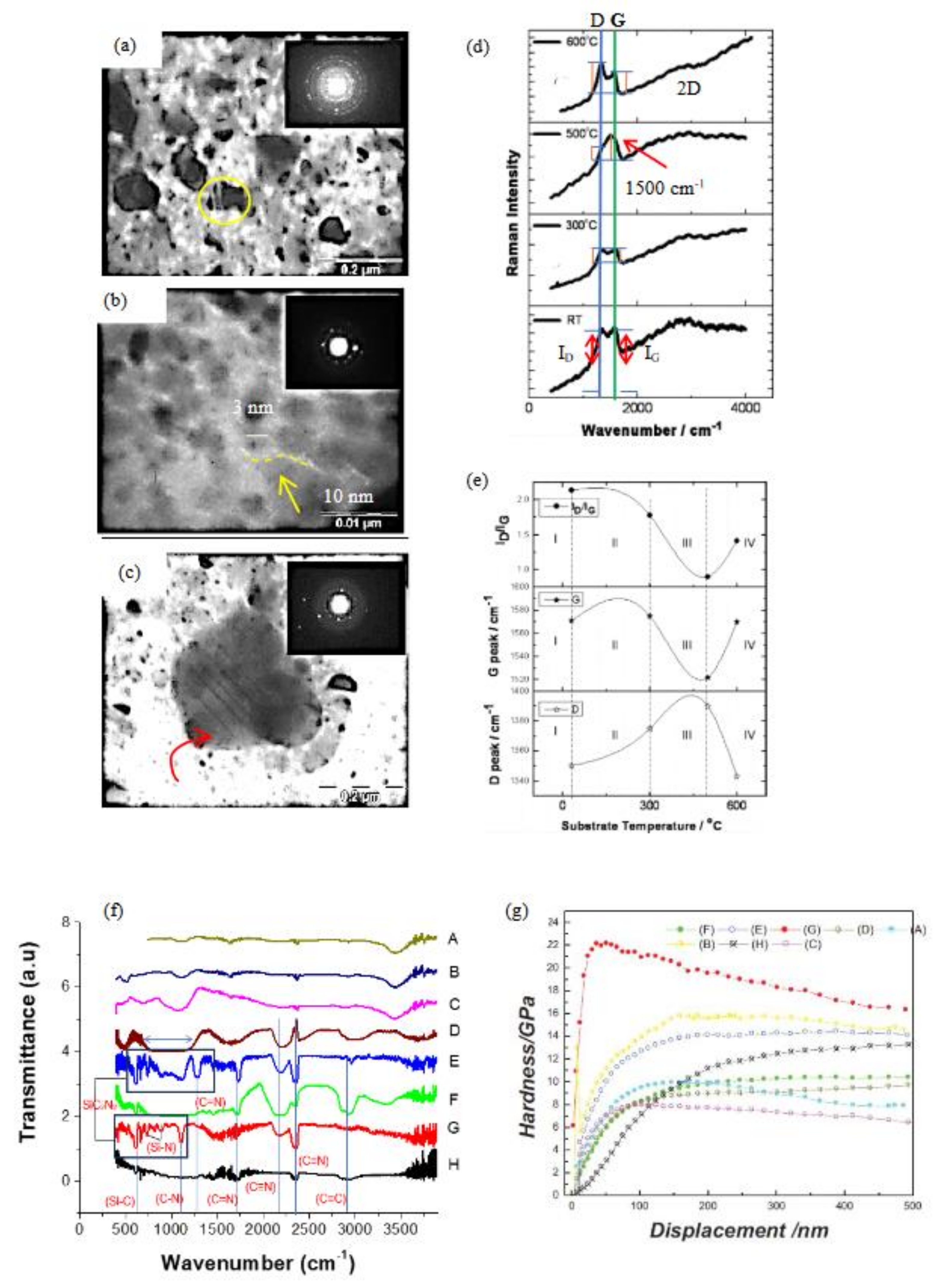
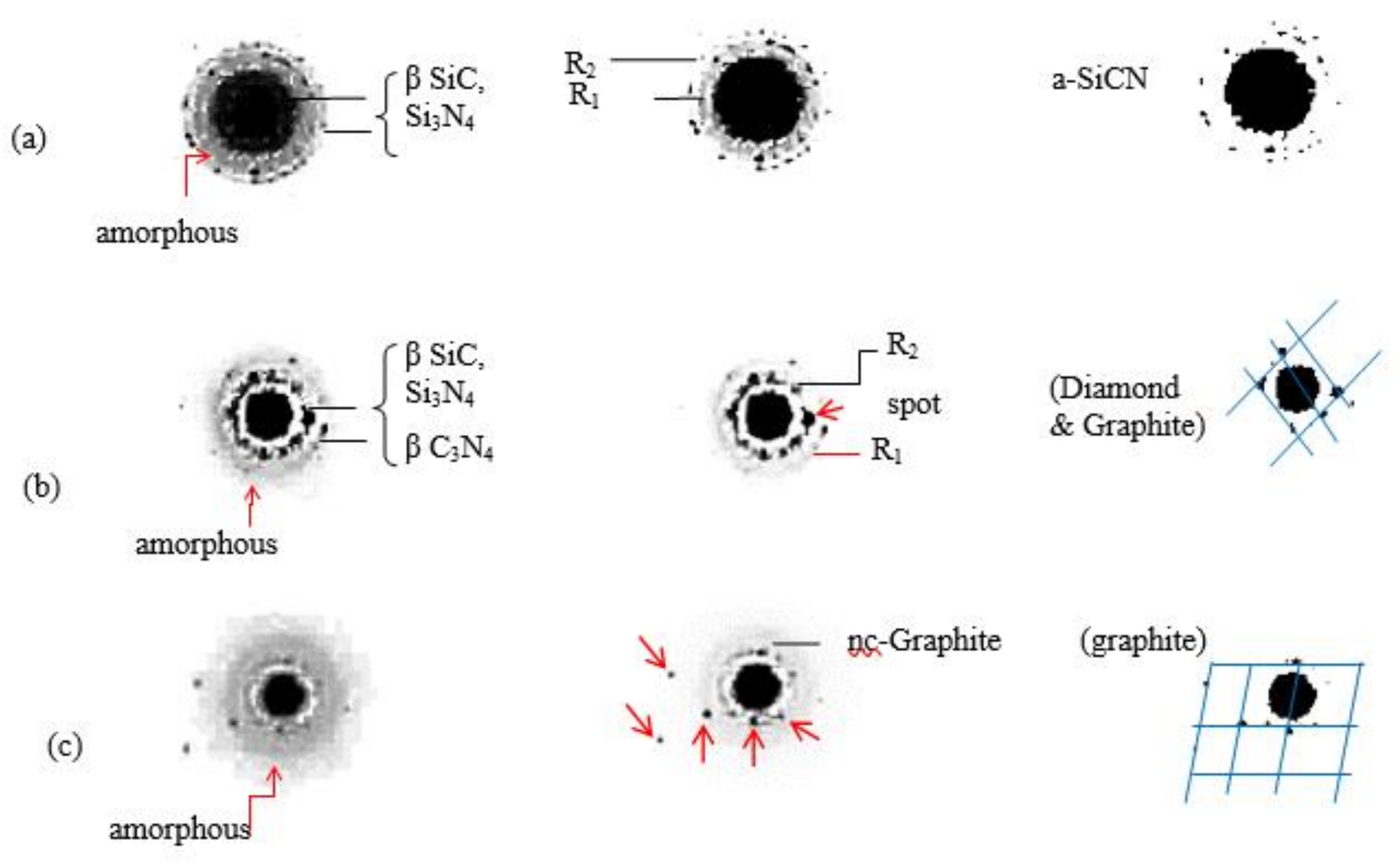
The heterogeneous crystallization with formation to near amorphous nanocrystallites and of larger dimensions can be seen in the TEM image along with the ring pattern observed in the SAED pattern. An initial increase in substrate temperature led to a transition from the nc-graphitic phase to amorphous carbon which reacted with Si and N and eventually formed the amorphous Si-C-N matrix. At higher temperatures, nucleation of nanosized crystallites of hard phases of β-Si3N4 and β-C3N4 occurred in the amorphous Si-C-N matrix (Figure 2a–c). The crystallite size varied between 2 to 20 nm on varying the substrate temperature from RT to 500 °C. However, on a further rise in temperature to 600 °C, an increase in the growth of the carbon phase due to the desorption of nitrogen at higher temperatures occurred, which led to a decrease in hardness [41,42,43]. The contrast of the images was changed to get a clear image of some of the structural features like twins as marked in the images inside a large crystallite which aroused due to strain getting developed in the film during film growth. The growth phenomena can be understood if we look at the corresponding SAED patterns given as insets for each of the cases. A ring pattern with bright spots along the circumference implies the initiation of nucleation of growth of crystallites on an amorphous base at RT. The bright spots are the diffraction spots coming from a set of planes. Stacking faults were observed as marked in the image with a circle. The nucleation and growth get intensified as the deposition temperature is increased evident from the higher intensity of the diffraction spots and not being dedicated to a circular pattern. This shows the co-existence of different phases at a time which is the prerequisite for a nanocomposite. The deviation from the circular nature gets even higher for a further temperature rise. The SAED pattern can be found to partially resemble a spot pattern to some extent. This shows the texture of the coating departing from its nanocrystalline nature and preferably getting inclined towards graphite which lowers the hardness as expected and observed. The patterns were inverted and analyzed with different contrast and brightness. The ring patterns depicting nanocrystalline β-SiC and Si3N4 on an amorphous (a-Si-C-N) along with graphitic phases can be observed in Figure 3a. The ring patterns were not continuous and looked like made up of broken lines indicating in homogenous size distribution of the crystallites as also evident from the microscopic image. No spot pattern was found even changing the pictorial parameters showing the crystallization to be in its nascent stage. At 500 °C where the highest hardness was observed, the ring patterns got fewer in numbers but more intense. These were due to the formation of nanocrystalline phases of β-C3N4 and to some extent diamond. These phases mainly grew on sp2 carbon domains The spot patterns observed in changing the contrast and brightness were due to larger crystallites of sp3 C (diamond) and sp2 C (graphite) (Figure 3b). The ring patterns were formed due to nanocrystalline graphite, got lowered in number as well as intensity at 600 °C, and spot patterns of graphitic phase due to larger graphitic crystals got prominent. The amorphous fraction also increased compared to the previous case (Figure 3c). This indicates preferential crystal growth of mainly graphite due to increased surface carbon diffusion which needs a thermodynamical perspective and shall be explored in due course.

3.4. The 4-Stage Model Based on Deposition Pressure

The Raman spectra of Si-C-N coatings deposited at different substrate temperatures are shown in Figure 2d. The spectra have been deconvoluted and discussed in detail previously [42]. The transition from one carbon form to another leading to the variation in hardness and modulus is due to the variation in sp2/sp3 carbon percentage and results in a shift in G (graphitic) and D(disorder) peak position and intensity. In the spectra for RT deposition, a G band position at 1571 cm−1 and a D band position at 1350 cm−1 are observed which corresponds to nc-graphite. The origin of these peaks is related to the total optic modes of graphite which is a sum of different modes as given in Equation (1).
Γ = A2u + 2B2g + E1u + 2E2g
The E2g modes are Raman active and are observed at 42 and 1581 cm−1. The A2u and E1u are IR active and observed at 867 and 1588 cm−1. The B2g modes are optically inactive. The E-symmetry modes have in-plane atomic displacement while the A and B modes have out-of-plane displacements
On increasing the temperature further, the crystallite size continues to lower further which results in the disappearance of the nc-graphitic phase and the formation of a-Si-C-N. The prominent separation between the D and G positions, which is the evidence of graphitization, gradually decreases with an increase in temperature and almost a single band formation at 1500 cm−1 occurs at 400 °C. This corresponds to the formation of sp3 hybridized ta-C in the form of nucleation and growth of β-C3N4 crystallites in the a+Si-C-N matrix. This results in an upper shift of the G band position as observed in the spectrum for coating deposited at 500 °C. The microstructural and structural changes discussed above on increasing the substrate temperature. At 600 °C however, a further increase in the G band position was observed. This is due to the growth of carbon crystallites and the formation of the nc-graphitic phase. An abnormal graphitization has also been reported for polymer-derived (PD) SiCN [49]. All these phenomena led to a 4-stage model based on the well-known 3-stage model by Tuinstra, J. L. Koenig [50] as shown in Figure 2e. The formation of nanocrystalline phases at different combinations of process parameters and their effect on the film hardness was also understood by FTIR spectra and Nanoindentation as shown in Figure 2f,g [43].
The FTIR peaks between 500–900 cm−1 were due to Si-C, Si-Nand C-N. The signatures of C=N were conformed by peaks at 1250 and 1750 cm−1. The peaks at 2200 and 2800 cm−1 were due to C≡N and C≡C respectively. The C-N bonds representing β-C3N4 caused the high hardness. A temperature rise was found to induce a higher percentage of C-N and C=N bonds which however decreased on increasing the temperature further to 600 °C, as the excess C got involved in C=C and C≡C bond formation resulting in graphitic phase formation causing a decrease in hardness. A higher pressure caused increased collisions between the adatoms and gas molecules also causing a decreased C-N percentage in the films [40].
Because carbon diffusion increases with temperature, it is quite likely that the crystallites generated are those of graphite, as determined by the Raman Spectra for a temperature change from 500 °C to 600 °C. The D peak, as previously stated, is caused not only by defects but also by the presence of carbon with various hybridizations—sp3(C-C) and sp (C≡C). The crystallite size also plays an important role, as evidenced by highly referenced papers. [50,51] The G peak was discovered to provide a wide range of location and intensity (relative to the D peak) alterations. The greatest movement in the G peak location was discovered at 500 °C, where it was observed at 1500 cm−1, causing a shift of around 100 cm−1 from the spectra observed at lower temperatures which is equivalent to 198.6 × 10⁻²³ J. A difference in the intensity of the D peak was prevalent. The initial diminishing followed by the sudden reappearance indicated amorphization followed by nucleation of near amorphous ultra-fine crystallites. At this stage, the coating has a unique combination of hard phases of β-SiC, Si3N4, CNx (α, β C3N4), and even a fraction of sp3 carbon which in totality can be called diamond-like nanocomposite (DLN) coatings. The hardness being inversely proportional to the ID/IG ratio was very high in this case [52]. The ID/IG is used for the determination of sp2 domains (L sp2, nm), average defect distance (LD. nm), and defect density (nD, cm−2) as per the following Equations (1)–(3) [53]. where the terms EL (in eV) and λL (in nm) are the energy and wavelength of the Laser source associated with the Raman spectrometer which was 2.33 eV and 532 nm as also mentioned in Section 2. The ID and IG terms mentioned are the integral intensity ratios that have been used to determine the parameters as given in Table 3. However, a qualitative analysis has been made using the height ratios as shown in the diagram. The sp2 domain size was 19 nm till 300 °C, increased to about 25 nm at 500 °C, and then again decreased to 14 nm at 600 °C. The average defect distance was again 14 nm initially, increased to 19 nm, and decreased to 10 nm. The defect density was 3 × 1011 cm −2 which reduced to 2.25 for 500 °C and again then increased to 4 for 600 °C. The parameters obtained from the height ratio therefore although having ambiguity in the values obtained for the initial temperatures, follow the same trend as that of the integral ratio values.
L s p 2 = 560 E L 4 I G I D
L D 2 = 2.4 × 10 9 λ L 4 I G I D
n D = 2.4 × 10 22 λ L 4 I D I G
Interestingly from the relations above the increase of the sp2 carbon domain causing the Occurrence of a concurrence with the diminished D peak at 500 °C can be seen. This is contrary to the hardness value trend we obtained. The explanation of the above fact can be proposed as follows. We must understand that there are other phases of Si-C and C-N as well which are also getting affected as we are changing the temperatures. The sp2 domain may therefore consist of near amorphous ultrafine nucleation of crystallites of these hard phases and to some extent diamond (sp3 C) as well. The shift of the G-peak towards lower wave numbers is evidence of higher amorphic nature [50]. The doublet D-G spectra are known as one photon spectra. The D and G arise due to breathing and stretching modes respectively in a hexagonal unit cell of carbon. The other modes associated with different bonding configurations can be found in ref [54]. The overtones around 3000 cm−1 which are called the 2D or G + G’ peaks in some instances are also known as two phonon spectra that occur due to electron density delocalization. The 2D peaks did not reveal themselves for the 500 °C indicating the existence of feeble electrical anharmonicity [55]. The possibility of the diamond phase percolating considering the high pressure in the vacuum chamber causes an inevitable increase in hardness. A rise in temperature causes graphitization, as the absorbed thermal energy is transferred to the internal crystal lattice of the diamond, it rearranges itself into graphite where a change in the potential energy surface by electrons in the crystal lattice may also be present [56]. It is also evidence of the formation much softer graphitic phase due to obtaining the D and G peak positions for graphite bearing its signature.
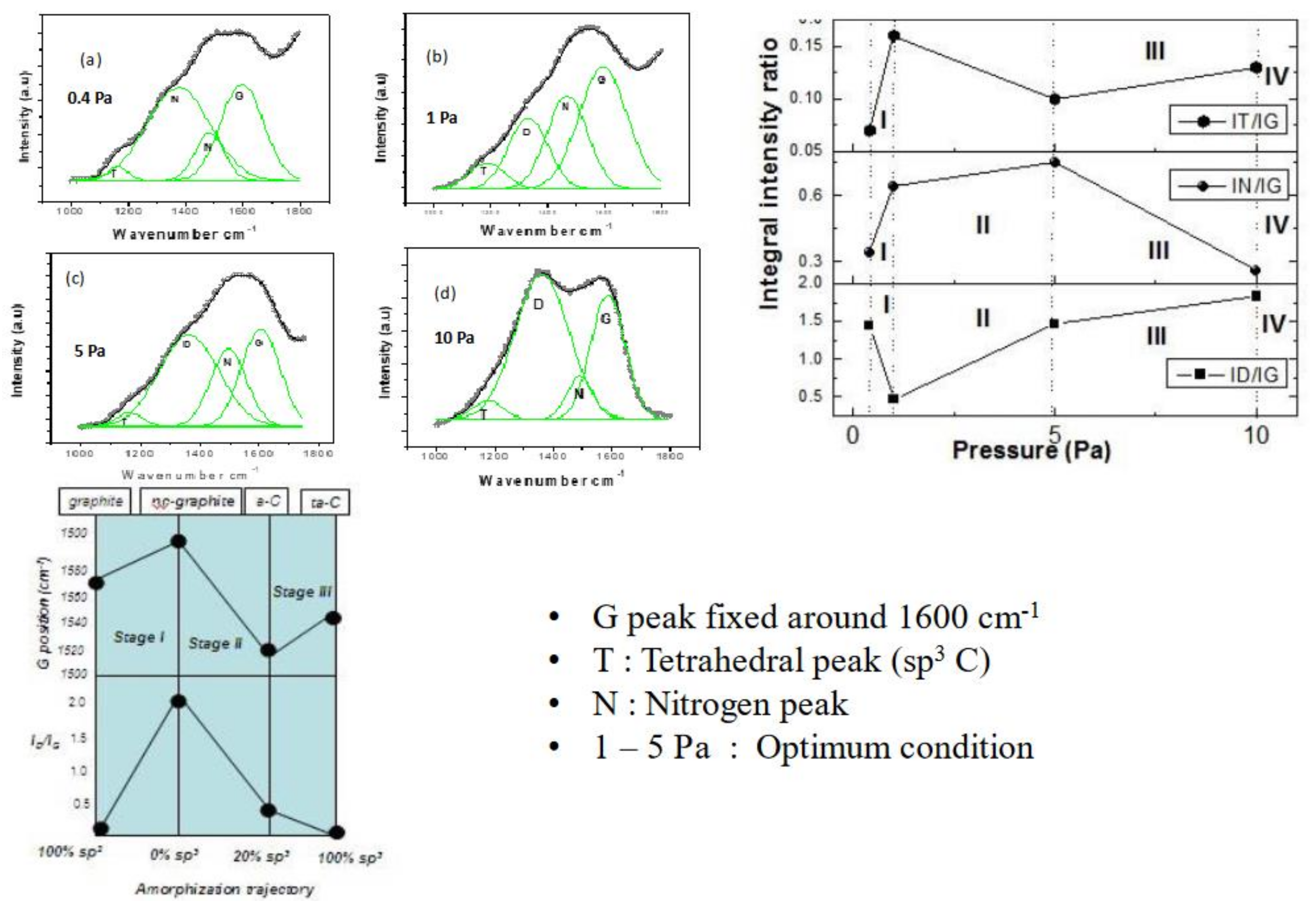
The deposition condition of 500 °C and 1 Pa N2-Ar pressure gives the highest hardness due to the formation of nan Ocrystallites like SiC, Si3N4, and even β-C3N4 giving a high hardness of 22 GPa from nanoindentation which can be considered sufficiently high taking into consideration the high sharpness of the Berkovich Indenter (cone angle ~ 70.3°). The Raman spectra of SiCN coatings deposited at different pressures are shown in Figure 4a–d. The deconvolution of the peaks was done and the ratio of the integral intensities corresponding to tetrahedral (IT), disorder (ID), and graphitic (IG) was platted concerning change in pressure forming a 3-stage model based on pressure as done previously based on temperature [42]. The IT/IG ratio indicating the ratio of sp3/sp2 carbon ratio was high in 1 Pa, reduced a bit for 5Pa and again increased with 10 Pa. This ratio showed that the formation of diamond-like carbon (DLC) phases was high in the case of 1 Pa pressure. The reason for the slight lowering of the ratio can be found in the phase diagram of SiCN (Figure 1a). The IN/IG ratio showed an increase with an increase in pressure to 1 to 5 Pa due to the formation of higher nitrogen-based phases like Si3N4 and C3N4. The ratio showed a decrease at a higher pressure of 10 Pa due to a decrease in the mean free path caused by the enhanced collision rate of the sputtered adatoms with the N2 gas molecules. The ID/IG ratio was also the lowest in the case of 1 Pa pressure. All these observations lead to the fact that 1 Pa is the optimized pressure for SiCN coatings as also observed earlier [42,43].

3.5. Microstructure

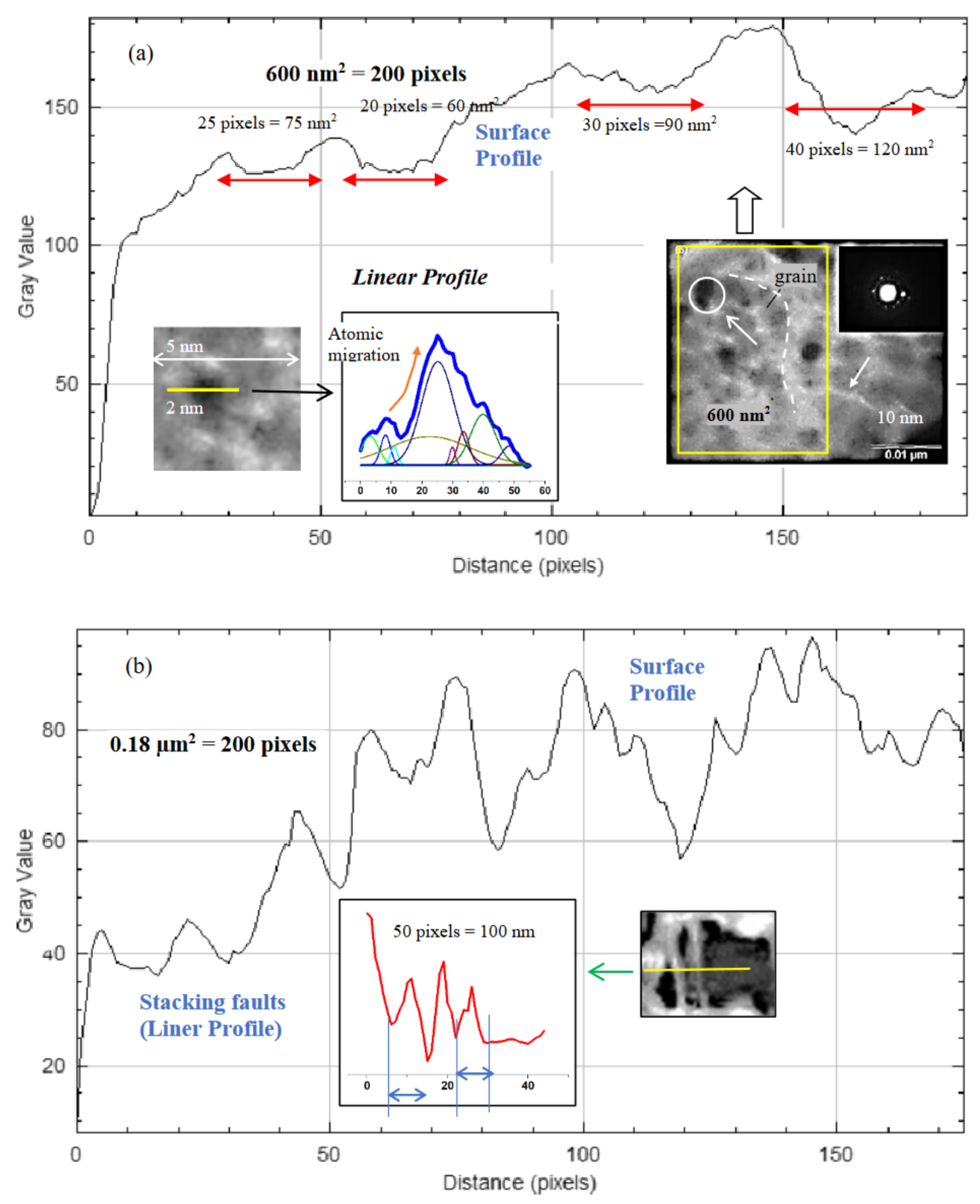
Image analysis of the TEM pictures revealed the nucleation and growth process involved during the deposition of the thin films. A reduced grain size results in enhanced mechanical properties. However, an extreme reduction in size, like the ones observed in the TEM image of coatings deposited at 500 °C showing crystallites of very small size (< 5 nm) may result in a decrease in mechanical strength due to inverse Hall-Petch relation. The image profile of the microstructure area of 600 nm2 marked (inset) is shown in Figure 5a. It should however be kept in mind that nucleation and growth are two separate phenomena. After the crystallites have nucleated, atomic migration makes them coalesce to form larger crystals and eventually grains, and it is the grain size d that matters for the applicability of the Hall-Petch relation. The crystallites observed to form are surrounded by smaller crystallites that have reached them by the migrating as indicated in the image. The process of this migration has also left trails as observed in the form of linear vacancy created. The atomic migration eventually will form grains, evidence of which can also be seen in the marked by broken lines. The line profile of one of the nucleated crystallites is shown separately. The figure was inversed to get upward peaks for the growth regions’ which were further deconvoluted into multiple peaks indicating small crystallites. These are regions adjacent to the main crystallites, where agglomeration of crystallites has taken place but has not undergone coalescence due to insufficient energy for atomic migration. The agglomeration caused by atomic vibration often leaves voids [57] These voids may be the epicenters of stress intensification and can cause crack generation and brittle failure. Post-deposition annealing may get rid of the voids to some extent and relieve the built-up interfacial stress. One may argue that a higher substrate temperature during deposition may be adopted instead. However, the hardness shall get compromised in that case as the growth of softer graphitic carbon (sp2) due to the excess carbon as shown in Figure 1b will enhance [42].
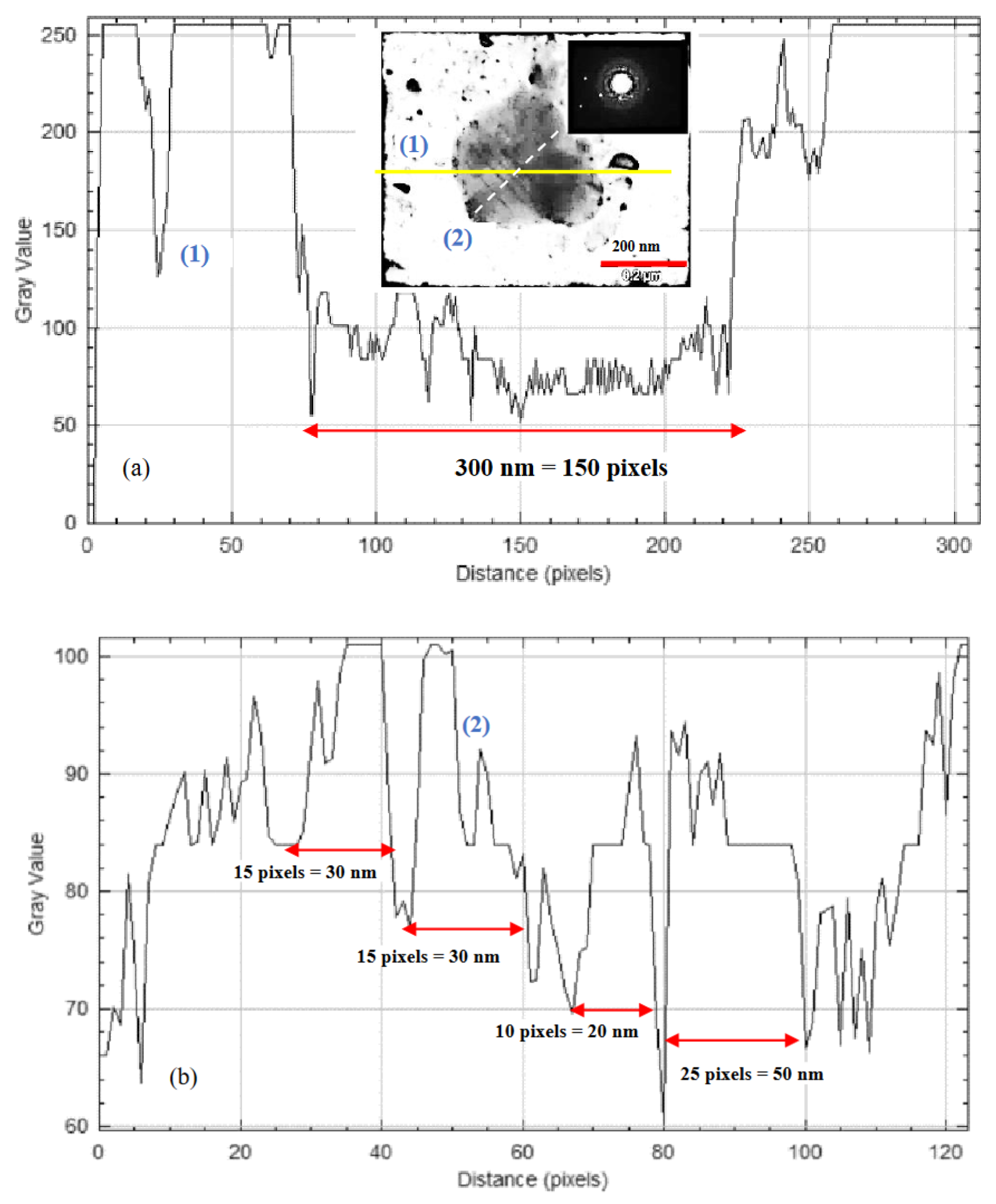
The surface profile of the image for RT deposition showed the peaks to be relatively higher in intensity indicating the effect of high temperature to be causing major atomic diffusion to create a homogenous distribution of the crystallites leading to lower and flatter intensity peaks distributed over different areas as marked (Figure 6a). The line profile of the stacking faults showed an average spacing of about 20 nm. (Figure 6b). For films deposited at 600 °C, the line profile of the large crystallite of 300 nm size is given in Figure 6a. The profile of the twins formed is shown separately with measured spacings (Figure 6b).

4. Conclusions

Nanocomposite Si-CN films are technologically important coatings used in microelectronic devices and as protective metallurgical coatings. The properties of these Si-C-N coatings deposited by magnetron sputtering were found to be strongly dependent upon the deposition parameters viz., N2-Ar pressure maintained in the vacuum chamber, substrate temperature The different ratios of phases of β-C3N4, Si3N4, and graphite in the film and the effective particle size at different deposition conditions affected the film properties [58,59].
The excess carbon in the structure being manifested itself in different forms viz. graphite, nc-graphite, and diamond based on the deposited pressure, affecting the film hardness. The transformation from amorphous to nanocrystalline ultra-fine growth of various phases followed by preferential crystal growth was reflected in the SAED patterns. A 4-stage model based on Raman spectra of coatings deposited at different pressure ranges like a previously existing model based on temperature was proposed. Image analysis of the microstructures showed the variation in nucleation and growth density of the crystallites. The research adds to the knowledge regarding the growth dynamics of Si-C-N being used in N/MEMS aerospace etc. It also builds a foundation for the study involving the inclusion of other elements in the composite improving and enhancing the versatility in the application of PDC-based Si-CN coatings and their derivatives.

Funding

No funding was received for conducting the research.

Data Availability Statement

Data are available from the corresponding author upon reasonable request.

Acknowledgments

The authors would like to acknowledge S. K. Mishra, CSIR-National Metallurgical Laboratory for experimental facilities.

Conflicts of Interest

The authors have no conflicts to disclose.

References

  1. Shah, S.R.; Raj, R. Mechanical Properties of a Fully Dense Polymer Derived Ceramic Made by a Novel Pressure Casting Process. Acta Mater. 2002, 50, 4093–4103. [Google Scholar] [CrossRef]
  2. Riedel, R.; Kleebe, H.-J.; Schönfelder, H.; Aldinger, F. A Covalent Micro/Nano-Composite Resistant to High-Temperature Oxidation. Nature 1995, 374, 526–528. [Google Scholar] [CrossRef]
  3. Ren, Z.; Mujib, S.B.; Singh, G. High-Temperature Properties and Applications of Si-Based Polymer-Derived Ceramics: A Review. Materials 2021, 14, 614. [Google Scholar] [CrossRef] [PubMed]
  4. Barrios, E.; Zhai, L. A Review of the Evolution of the Nanostructure of SiCN and SiOC Polymer Derived Ceramics and the Impact on Mechanical Properties. Mol. Syst. Des. Eng. 2020, 5, 1606–1641. [Google Scholar] [CrossRef]
  5. Lin, X.; Gong, H.; Chen, Z. Fabrication of SiCN (Fe)/Al2O3 wave-absorbing ceramics with enhanced electromagnetic performance. Ceram Int. 2023, 49, 23851–23863. [Google Scholar] [CrossRef]
  6. Geng, T.B.; Yu, G.Y.; Shao, G.F.; Huang, X.G. Enhanced electromagnetic wave absorption properties of ZIF-67 modified polymer-derived SiCN ceramics by in situ construction of multiple heterointerfaces. Rare Metals 2023, 42, 1635–1644. [Google Scholar] [CrossRef]
  7. Xue, J.; Hu, S.; Li, X.; Li, F.; Liu, Y.; Wei, H. Enhanced microwave absorbing properties of Y2O3 modified PDC SiCN ceramics with heterogeneous amorphous interface. Journal of Alloys and Compounds 2023, 931, 167499. [Google Scholar] [CrossRef]
  8. Han, D., You, G., Zhang, Y., Tian, H., He, J., Liang, J.,… & Shao, G. Increased microwave absorption property of porous Si3N4 ceramics by loading polymer-derived SiCN for a multifunctional design. Journal of Materials Chemistry C 2023, 11, 6130–6137.
  9. Wu, C., Fu, Y., Zeng, Y., Chen, G., Pan, X., Lin, F.,… & Hai, Z. Ultrafast high-temperature sintering of polymer-derived ceramic nanocomposites for high-temperature thin-film sensors. Chemical Engineering Journal 2023, 463, 142518.
  10. Chen, G., Zeng, Y., Zhao, F., Wu, C., Pan, X., Lin, F.,… & Hai, Z. Conformal fabrication of functional polymer-derived ceramics thin films. Surf Coat Technol 2023, 464, 129536.
  11. Li, L., He, Y., Xu, L., Shao, C., He, G., Sun, D., & Hai, Z. Oxidation and Ablation Behavior of Particle-Filled SiCN Precursor Coatings for Thin-Film Sensors. Polymers 2023, 15, 3319.
  12. Cui, Z., Chen, X., Li, X., & Sui, G. Thin-film temperature sensor made from polymer-derived ceramics based on laser pyrolysis. Sensors and Actuators A: Physical 2023, 350, 114144.
  13. Ma, K., Bekiaris, N., Ramaswami, S., Ding, T., Probst, G., Burggraf, J., & Uhrmann, T. 0.5 ¼m Pitch Wafer-to-wafer Hybrid Bonding with SiCN Bonding Interface for Advanced Memory. In Proceedings of the IEEE 73rd Electronic Components and Technology Conference (ECTC); 2023; pp. 1110–1114.
  14. Stiharu, I., Andronenko, S., Zinnatullin, A., & Vagizov, F. SiCNFe Ceramics as Soft Magnetic Material for MEMS Magnetic Devices: A Mössbauer Study. Micromachines 2023, 14, 925.
  15. Xia, X., Chiang, C.C., Gopalakrishnan, S.K., Kulkarni, A.V., Ren, F., Ziegler, K.J., & Esquivel-Upshaw, J.F. Properties of SiCN Films Relevant to Dental Implant Applications. Materials 2023, 16, 5318.
  16. Choi, H.J.; Lu, K. A high compatibility SiOCN coating on stainless steel. Journal of Materials Science 2023, 58, 3790–3801. [Google Scholar] [CrossRef]
  17. Liu, K., Peng, W., Han, D., Liang, Y., Fan, B., Lu, H.,… & Shao, G. Enhanced piezoresistivity of polymer-derived SiCN ceramics by regulating divinylbenzene-induced free carbon. Ceramics International 2023, 49, 2296–2301.
  18. Sulyaeva, V.S., Kolodin, A.N., Khomyakov, M.N., Kozhevnikov, A.K., & Kosinova, M.L. Enhanced Wettability, Hardness, and Tunable Optical Properties of SiCxNy Coatings Formed by Reactive Magnetron Sputtering. Materials 2023, 16, 1467.
  19. Tomastik, J.; Ctvrtlik, R.; Ingr, T.; Manak, J.; Opletalova, A. Effect of Nitrogen Doping and Temperature on Mechanical Durability of Silicon Carbide Thin Films. Sci. Rep. 2018, 8. [Google Scholar] [CrossRef] [PubMed]
  20. Bernauer, Jan & Petry, Nils-Christian & Thor, Nathalie & Kredel, Samuel & Teppala, Dharma & Galetz, Mathias & Lepple, Maren & Pundt, Astrid & Ionescu, Emanuel & Riedel, Ralf. Exceptional Hardness and Thermal Properties of SiC/(Hf,Ta)C(N)/(B)C Ceramic Composites Derived from Single-Source Precursor. Advanced Engineering Materials 2024. [CrossRef]
  21. Bernauer, Jan & Kredel, Samuel & Ionescu, Emanuel & Riedel, Ralf. Polymer-derived ceramic Coatings with Excellent Thermal Cycling Stability. Adv Eng Mater 2024. [CrossRef]
  22. Thor, Nathalie & Bernauer, Jan & Petry, Nils-Christian & Ionescu, Emanuel & Riedel, Ralf & Pundt, A. & Kleebe, Hans-Joachim. Microstructural Evolution of Si(HfxTa1-x)(C)N Polymer-Derived Ceramics upon High-Temperature Anneal. J Eur Ceram Soc 2022, 43, 1417–1431.
  23. Zhu, Runqiu & Jin, Shuo & Xing, Ruizhe & Song, Yan & Yu, Zhen & Liu, Ziyu & Kong, Jie. Nanoparticles-doped polymer-derived SiCN ceramic with enhanced mechanical properties and electromagnetic wave absorption. Journal of the American Ceramic Society 2024. [CrossRef]
  24. Wang, Beibei & Liu, Xingmin & Liu, Yue & Fu, Qiangang & Riedel, Ralf. Single-source-precursor synthesized SiCN/MWCNT nanocomposites with improved microwave absorbing performance. Journal of Materials Science: Materials in Electronics 2024, 35. [CrossRef]
  25. Ye, Xiao-Juan & Wang, Xiao-Han & Cao, Hong-Bao & Lu, Zheng & Liu, Chun-Sheng. Penta-SiCN monolayer is a well-balanced performance anode material for Li-ion batteries. Physical Chemistry Chemical Physics 2023, 25. [CrossRef]
  26. Chiang, Chao-Ching & Xia, Xinyi & Craciun, Valentin & Rocha, Mateus & Camargo, Samira & Rocha, Fernanda & Gopalakrishnan, Sarathy Kannan & Ziegler, Kirk & Ren, Fan & Esquivel-Upshaw, Josephine. Enhancing the Hydrophobicity and Antibacterial Properties of SiCN-Coated Surfaces with Quaternization to Address Peri-Implantitis. Materials 2023, 16, 5751. [CrossRef]
  27. Qiang Yan, Siyao Chen, Haofan Shi, Xiaofei Wang, Songhe Meng, Jinping Li, Fabrication of polymer-derived SiBCN ceramic temperature sensor with excellent sensing performance. ournal of the European Ceramic Society 2023, 43, 7373–7380. [CrossRef]
  28. Yan, Yuangao & Fei, Xuan & Huang, Liuying & Yu, Yuxi & Wen, Yichen & Zhao, Gang. Effect of BN content on the structural, mechanical, and dielectric properties of PDCs-SiCN(BN) composite ceramics. J Am Ceram Soc. 2023, 106, 6951–6961.
  29. Anand, R & Lu, Kathy & Nayak, Bibhuti & Behera, Shantanu. Structural evolution and oxidation resistance of polysilazane-derived SiCN-HfO 2 ceramics. J Am Ceram Soc. 2023, 107, 1657–1668.
  30. Chery, Emmanuel & Fohn, Corinna & De Messemaeker, Joke & Beyne, Eric. Reliability Challenges in Advanced 3D Technologies: The Case of Through Silicon Vias and SiCN–SiCN Wafer-to-Wafer Hybrid-Bonding Technologies. IEEE Tran on Device and Mater Rel 2023, 23, 615–622.
  31. Ramlow, Heloisa & Marangoni, Cintia & Motz, Günter & Singh, Gurpreet & Machado, Ricardo. Electrochemical performance of SiCN embedded carbon (SiCN–C) fiber mat electrodes for lithium-ion battery: Electrospinning polysilazane in air or protective atmosphere. Open Ceramics 2023, 14, 100351.
  32. Ramlow, Heloisa & Souza, Graciano & Fonseca, Mikael & Raizer, Adroaldo & Rambo, Carlos & Machado, Ricardo. Lightweight and flexible nanostructured C/SiCN nanofiber nonwoven for electromagnetic reflection shielding of 5G C-Band frequencies. Materials in Electronics 2023, 34, 1631.
  33. Ramlow, Heloisa & Ribeiro, Luiz & Schafföner, Stefan & Motz, Günter & Machado, Ricardo. (2024). Thermo-oxidative resistance of C-rich SiCN(O) nonwovens influenced by the pretreatment of the silazane. J. Europ Ceram Soc 2024. [CrossRef]
  34. d’Eril, Marco & Graczyk-Zajac, Magdalena & Riedel, Ralf. On the Reversible Sodium Plating/stripping Reaction in Porous SiCN(O) Ceramic: A Feasibility Study. Batteries & Supercaps 2023, 6, e202200491.
  35. Li, Qiang & Chen, Cheng & Wang, Mingge & Lv, Yaohui & Mao, Yulu & Xu, Manzhang & Wang, Yingnan & Wang, Xuewen & Zhang, Zhiyong & Wang, Shouguo & Zhao, Wu & Stiens, J. Study on Photoelectricity Properties of SiCN Thin Films Prepared by Magnetron Sputtering. J Mater Res Technol. 2021, 15, 460–467.
  36. Jiang, Minming & Xu, Ke & Liao, Ningbo & Zheng, Beirong. Effect of sputtering power on piezoresistivity and interfacial strength of SiCN thin films prepared by magnetic sputtering. Ceram Int. 2021, 48, 2112–2117.
  37. Das, S., Kumar, D., Borah, R. et al. Impact of elevated temperature over different properties of CVD SiCN coating developed in Nitrogen gas atmosphere. Silicon 2022, 14, 9643–9657. [CrossRef]
  38. Haofan, Shi & Li, Jinping & Zhang, Gaoming & Meng, Songhe. Effect of free carbon content changed by divinylbenzene on the conductivity of SiCN ceramic. J. Mater Sci: Materials in Electronics 2023, 34, 1401.
  39. Matar, Samir & Etourneau, Jean & Solozhenko, Vladimir. Novel (Super)Hard SiCN from Crystal Chemistry and First Principles. Silicon 2022, 15, 511–520.
  40. Bhattacharyya, AS, Growth of stable SiC2N2-Si2CN4 phases during nitrogen incorporated sputter deposition of silicon carbide. Chemical Physics Impact 2024, 8, 100454. [CrossRef]
  41. Bhattacharyya, A.S.; Mishra S.K.; Mukherjee, S.; Hot Properties. Eur. Coat. J. 2009, 3, 108–114.
  42. Bhattacharyya, A.S.; Mishra, S.K. Raman Studies on Nanocomposite Silicon Carbonitride Thin Film Deposited by r.f. Magnetron Sputtering at Different Substrate Temperatures. J. Raman Spectrosc. 2010, 41, 1234–1239. [CrossRef]
  43. Bhattacharyya, AS Mishra, SK Mukherjee, S. Correlation of structure and hardness of rf magnetron sputtered silicon carbonitride films. J. Vac. Sci. Technol A 2010, 28, 505–509. [CrossRef]
  44. R. Dash, K. Bhattacharyya, A.S. Bhattacharyya. Fracture associated with static and sliding indentation of multicomponent hard coatings on silicon substrates. Fatigue & Fracture of Engineering Materials & Structures 2023, 46, 1641–1645.
  45. Arnab Sankar Bhattacharyya, Kushal Bhattacharyya, Effect of loading rate and coating thickness on wear and adhesion during sliding indents of Si–C–N/glass coatings useful for automotive applications. Results in Surfaces and Interfaces 2024, 100196. [CrossRef]
  46. Choi, H.J., & Lu, K. A high compatibility SiOCN coating on stainless steel. Journal of Materials Science 2023, 58, 3790–3801.
  47. Mishra, SK, Bhattacharyya, AS, Effect of substrate temperature on the adhesion properties of magnetron sputtered nano-composite Si–C–N hard thin films. Materials Letters 2008, 62, 398–402. [CrossRef]
  48. Bhattacharyya, A S, Modeling of sputter-based atomic layer deposition with altered parameters. Materials Today Comm 2024, 38, 107697. [CrossRef]
  49. Wu, C., Lin, F., Pan, X., Chen, G., Zeng, Y., Xu, L., … & Hai, Z. Abnormal Graphitization Behavior in Near-Surface/Interface Region of Polymer-Derived Ceramics. Small 2023, 19, 2206628.
  50. Tuinstra, F.; Koenig, J.L. Raman Spectrum of Graphite. J. Chem. Phys 1970, 53, 1126. [Google Scholar] [CrossRef]
  51. Ferrari, A.C.; Robertson, J. Interpretation of Raman spectra of disordered and amorphous carbon. Physical Review B 2000, 61, 14095. [Google Scholar] [CrossRef]
  52. Santra, TS, Liu CH, Bhattacharyya, TK, Patel, P, Barik TK, Characterization of diamond-like nanocomposite thin films grown by plasma enhanced chemical vapor deposition. Appl. Phys. 2010, 107, 124320. [CrossRef]
  53. Sharma, R Chadha, N. Saini, P. Determination of defect density, crystallite size and number of graphene layers in graphene analogs using X-ray diffraction and Raman spectroscopy. Ind J Pure & Appl Phy 2017, 55, 625–629.
  54. Varsanyi, G. Vibrational Spectra of Benzene Derivatives, Academic Press: New York, NY, USA, 1969.
  55. Sheka, E.F.; Golubev, Y.A.; Popova, N.A. Graphene Domain Signature of Raman Spectra of sp2 Amorphous Carbons. Nanomaterials 2020, 10, 2021. [Google Scholar] [CrossRef] [PubMed]
  56. Franz Tavella, Hauke Höppner, Victor Tkachenko, Nikita Medvedev, Flavio Capotondi, Torsten Golz, Yun Kai, Michele Manfredda, Emanuele Pedersoli, Mark J. Prandolini, Nikola Stojanovic, Takanori Tanikawa, Ulrich Teubner, Sven Toleikis, Beata Ziaja, Soft x-ray induced femtosecond solid-to-solid phase transition. High Energy Density Physics 2017, 24, 22–27.
  57. Nagano, F., Inoue, F., Phommahaxay, A., Peng, L., Chancerel, F., Naser, H.,… & Iacovo, S. Origin of Voids at the SiO2/SiO2 and SiCN/SiCN Bonding Interface Using Positron Annihilation Spectroscopy and Electron Spin Resonance. ECS Journal of Solid-State Science and Technology 2023, 12, 033002.
  58. AS Bhattacharyya, Nanocomposite Si-C-N coatings, arXiv:1608.05667 [cond-mat.mtrl-sci].
  59. A.S. Bhattacharyya, Nanocomposite Si-C-N coatings, 2018 ISBN 978-613-8-38960-6 Lap-Lambert Academic.
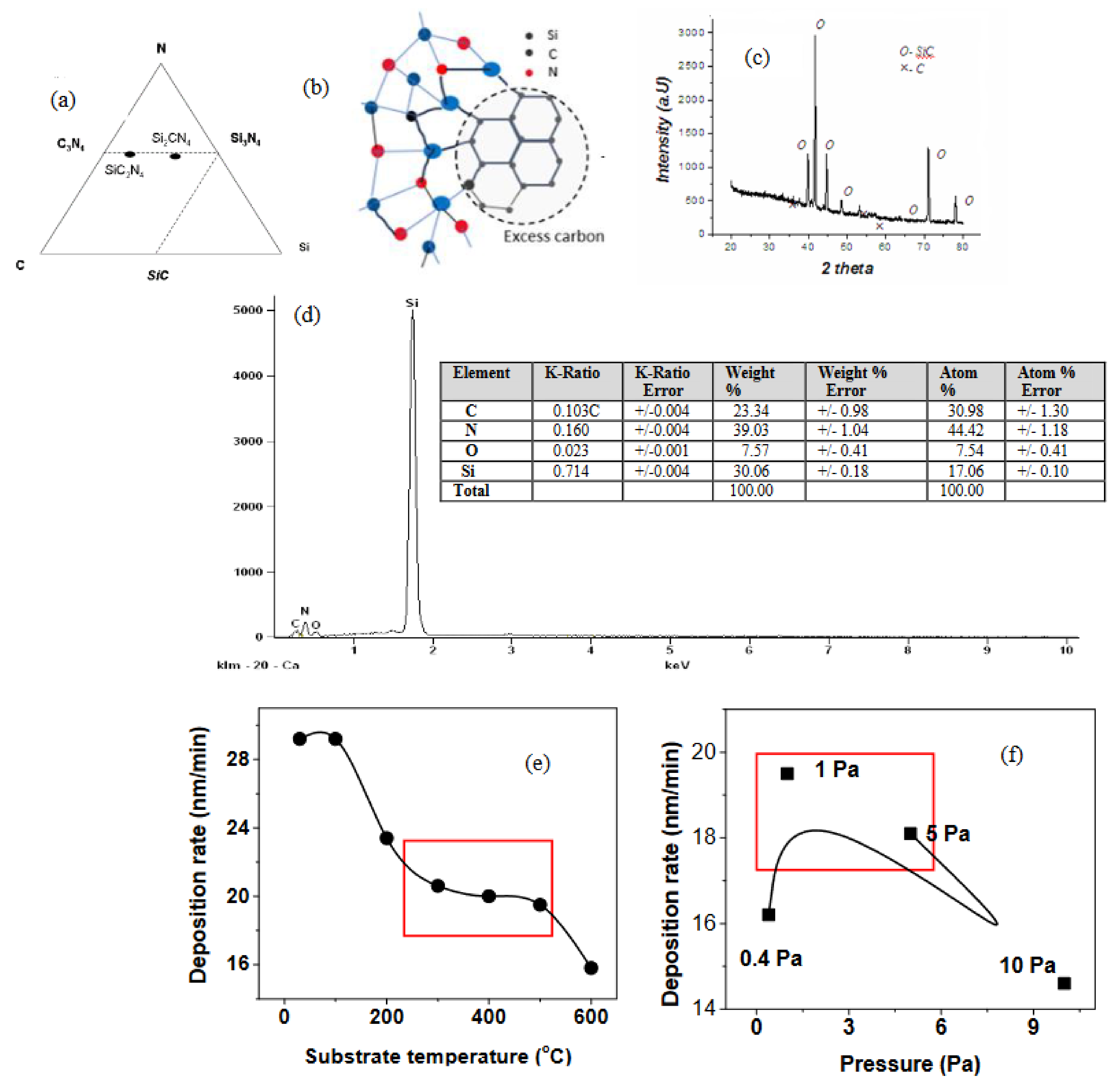
Figure 1. (a) Ternary phase diagram of Si-C-N (b) structure of Si-C-N with excess carbon (c) XRD of SiC target used for sputtering (c) and its EDAX showing the elemental compositions of the SiCN film. Variation of deposition rate with (d) substrate temperature and (e) pressure with areas marked giving coatings of higher.
Preprints 102654 g001
Figure 2. TEM image for SiCN films deposited at (a) RT (b) 500 °C and (c) 600 °C (d) Raman spectra (e) 4-stage model (Reprinted with permission from J. Raman. Spec. 41, 1234. Copyright 2010 John Wiley and Sons. [43]) (f) FTIR spectra [40] and (g) Nanoindentation hardness of Si-C-N films deposited at different conditions as per Table 1 (Reprinted with permission from J. Vac. Sc. Technol A 28, 505. Copyright 2010 American Vacuum Society. [44], CC BY open access [39]).
Preprints 102654 g002
Figure 3. SAED patterns for Si-C-N coatings deposited at (a) RT (b) 500 °C and (c) 600 °C with variable contrast and brightness showing a mixture of polycrystalline phases of β-SiC, Si3N4, β-C3N4. amorphous carbon, nc-graphite, and single crystalline graphite.
Preprints 102654 g003
Figure 4. Raman spectra of SiCN deposited with 500 °C and 400 W power at (a) 0.4 Pa (b) 1Pa (c) 5 Pa and (d) 10 Pa pressure with (e) 4 stage model based on the integral intensity ratio (f) Ferrari-Robertson 3 stage model as reference [51].
Preprints 102654 g004
Figure 5. (a) The surface profile of the TEM image for 500 °C deposition temperature and 1 Pa pressure as marked in the inset showing regions of crystallization (dark regions and profile depressions) and the linear profile of one crystallite (2 nm width) deconvoluted into multiple peaks depicting the process of coalescence due to atomic migration leaving void regions-marked by dotted lines (b) Surface profile of TEM image show in the inset for deposition carried out at RT along with the linear profile of the stacking fault as marked in the inset.
Preprints 102654 g005
Figure 6. (a) The profile as per line (1) of the enlarged crystallite formed as observed in the TEM image for 600 °C deposition temperature (b) as per line (2) indicating the formation of twins with measured spacings.
Preprints 102654 g006
Table 1. PDC and SiCN composites coatings: some recent reports.
S. No Composites/Coatings Properties Reference
1. SiC/(Hf,Ta)C(N)/(B)C;
SiHfTa(B)CN coatings;
Exceptional high hardness and thermal cycle stability; crack-free; amorphous, good adhesion [20,21]
2. Si(HfxTa1-x)(C)N residual carbon triggered decomposition reaction, resulting in the formation of Transition Metal Carbides, gaseous nitrogen and SiC, tetragonal hafnium oxide (t-HfO2) within the SiCN matrix-improved phase stability and oxidation resistance [22,29]
3. Ni–Fe–C/HfO2/SiCN;
SiCN/MWCNT
metal-organic framework (Ni–Fe–MOF) and hafnium dioxide (HfO2) nanoparticles; improved brittleness and EM wave absorption; MWCNT-COOH increased the interfacial polarization loss and the conduction loss, improving microwave absorbing performance. [23,24]
4. Penta-SiCN monolayer; SiCN embedded carbon (SiCN–C); Porous SiCN(O) low diffusion energy barrier and robust wettability useful in anode material for Li-ion batteries; stable cycling with a charge capacity, Reversible Na Plating/stripping Reaction for sodium metal batteries [25,31,34]
5. SiCN-coated implants Hydrophobicity and Antibacterial Properties, replacing Ti implants to avoid Peri-implantitis [26],
6. PDC SiCN Free carbon enriched interface, high conductivity, strain gauge [49]
7. polymer-derived SiBCN;
PDCs-SiCN(BN)
High-temperature sensing due to good thermomechanical properties, hexagonal boron nitride (h-BN) with weakened polarization relaxation behavior, reduced porosity, and resistance to crack expansion causes low dielectric loss and high-temperature resistance [27,28]
8. SiCN–SiCN wafer-to-wafer hybrid-bonding next generation of 3D Systems-on-Chip with interconnect densities above 10 mm−2 [30]
9. C/SiCN and SiCN(O) nanofiber, nonwoven tunable electrical conductivity, EM reflection shielding in the 5G C-band, and
thermo-oxidation resistance
[32,33]
10. Sputtered SiCN coatings Photoelectric properties, SiCN-based MEMS pressure sensors. [35,36]
11. CVD-grown SiCN coatings Increased intensity of Si-N-Si, decreased crystallite size with temperature along with increased hardness and modulus [37],
Table 2. Deposition rate and corresponding hardness of Si-C-N thin films (Adapted with permission from J. Vac. Sc. Technol A 28, 505. Copyright 2010 American Vacuum Society. [44]).
Deposition
Conditions
Temp(°C) Time (min) t(μm) Rate
(nm/min)
Hardness
(GPa)
1 Pa
400 W
RT 120 3.5 29.2 10
100 120 3.5 29.2 -
200 150 3.5 23.4 -
300 180 3.7 20.6 14
400 210 4.2 20.0 -
500 210 4.1 19.5 22
600 240 3.8 15.8 8
400 W
500 °C
Pressure
(Pa)
Time (min) t(μm) Rate
(nm/min)
Hardness
(GPa)
0.4 240 3.9 16.2 13
1 210 4.1 19.5 22
5 210 3.8 18.1 -
10 240 3.5 14.6 -
500 °C Power
(W)
Time (min) t(μm) Rate
(nm/min)
Hardness
(GPa)
1 Pa 200 240 3.5 14.6 9
300 210 3.9 18.6 15
10 Pa 400 210 3.5 16.7 7
Table 3. Domain size, defect distance, and density obtained from Raman spectra.
Temperature
(°C)
ID/IG
(Integral)
ID/IG
(Height)
L s p 2
(nm)
L D
(nm)
n D × 1011 (cm−2)
30 2.25 1.0 8.5 6 6.7
300 1.75 1.0 11 8 5.2
500 0.5 3/4 38 28 1.5
600 1.3 4/3 15 11 3.9
Pressure
(Pa)
ID/IG
(integral)
ID/IG
(height)
L s p 2 (nm) L D
(nm)
n D × 1011
(cm−2)
0.4 1.5 - 13 9 4.5
1.0 0.5 - 38 28 1.5
5.0 1.5 - 13 9 4.5
10 1.85 - 7 7.5 5.6
Disclaimer/Publisher’s Note: The statements, opinions and data contained in all publications are solely those of the individual author(s) and contributor(s) and not of MDPI and/or the editor(s). MDPI and/or the editor(s) disclaim responsibility for any injury to people or property resulting from any ideas, methods, instructions or products referred to in the content.
Copyright: This open access article is published under a Creative Commons CC BY 4.0 license, which permit the free download, distribution, and reuse, provided that the author and preprint are cited in any reuse.
Prerpints.org logo

Preprints.org is a free preprint server supported by MDPI in Basel, Switzerland.

Subscribe

© 2024 MDPI (Basel, Switzerland) unless otherwise stated