1. Introduction
One of the emerging subjects to be developed for future infrared (IR) applications is multiband IR detection to identify the unique footprint of a target and increase the probability of detection and identification of imminent threats [
1,
2,
3,
4]. Semiconductor band structure engineering permits various implementations of multiband IR detectors using a series of heterojunctions (HJs) that can be designed with a detailed understanding of carrier transport in the electronic band structure. Multiband IR photon detectors with HJs have been typically implemented with low bandgap (
) materials like HgCdTe [
5,
6,
7], which has a tunable
and a small change of lattice constant with CdTe mole fraction. More recently, another tunable
material class, type II superlattices (T2SLs) [
1,
2,
3,
4] has emerged as an alternative to HgCdTe.
A T2SL is an artificial material with variable
, which may be controlled by the thicknesses of, for example, InAs and GaSb layers forming the superlattice. One of interesting features of an InAs/GaSb T2SL is the small valence band offset (VBO) between the two materials while permitting the realization of various energy bandgaps [
8,
9], allowing the ready development of nBn unipolar barrier IR detectors. Indeed, this feature provides a major degree of freedom to design various devices including multiband IR detectors with different
T2SL materials, and facilitates bandgap engineering to implement various novel devices that could open new horizons.
nBn unipolar barrier IR detectors are a recent achievement aiding the utilization of T2SLs since they can attain performance superior to conventional photoconductive detectors [
8,
9,
10,
11,
12] and photovoltaic devices with the same materials [
13,
14,
15]. The role of a unipolar barrier is to block the flow of majority carriers without hindering the photogenerated minority carriers’ movement. This feature is very similar to a reverse biased p-n junction, which is the basic type of photovoltaic IR detector. A major feature of nBn’s in comparison with photovoltaic IR detectors is that they can suppress generation-recombination and tunneling dark currents arising in the depletion regions of conventional p-n junctions, potentially resulting in higher sensitivity and/or a higher operating temperature with same sensitivity [
8,
11,
13].
A sequential readout dual-band IR detector with InAs/GaSb T2SL materials is simply realized by the change of nBn to NBn, where the capital letter N means a larger
material than the lowercase n, both being T2SLs. An NBn, bias selectable dual-band IR detector uses photogenerated minority carriers, namely holes, as the signal carriers in both n-type materials. An NBn dual-band IR detector has great simplicity in structure and operation. Its three layers are enough to form a good dual-band IR detector, and the detection band can be selected by simple bias switching. Another T2SL dual-band IR detector structure is an n-i-p-p-i-n device, which can be designed to be simultaneously sensitive to radiation at 3-4
m and 4-5
m [
1,
16,
17].
In this paper, a novel dual-band barrier IR detector (DBIRD) using T2SLs is introduced. The DBIRD utilizes a unipolar electron barrier to block electron flow in the larger channel and a unipolar hole barrier to block hole flow in the smaller one. A detailed design procedure for a DBIRD is presented. A DBIRD modeling process to simulate its performance is also described. To assure proper operation of a DBIRD and to estimate its electrical and optical performances, a DBIRD for middle and long wavelength (MW/LW) dual-bands detection is designed and modeled. The simulations show that the DBIRD photoresponses, such as quantum efficiency (QE), responsivity and detectivity, are similar to those in previous studies of single band IR detectors with the same T2SLs.
2. Materials and Methods
2.1. DBIRD Design
A DBIRD consists of two consecutive barrier photodetectors. Each consists of three sequential T2SL regions. The blue channel (BC) device must be optically ahead of the red channel (RC) one. In the sequence of the incident IR radiation, the BC device has a n-type absorber, the same type electron barrier, and a p-type region, while the RC device has a p-type absorber, the same type hole barrier, and a n-type region, together making up n-B
n-p-B
p-n as a whole, where B
x means barrier with doping type x.
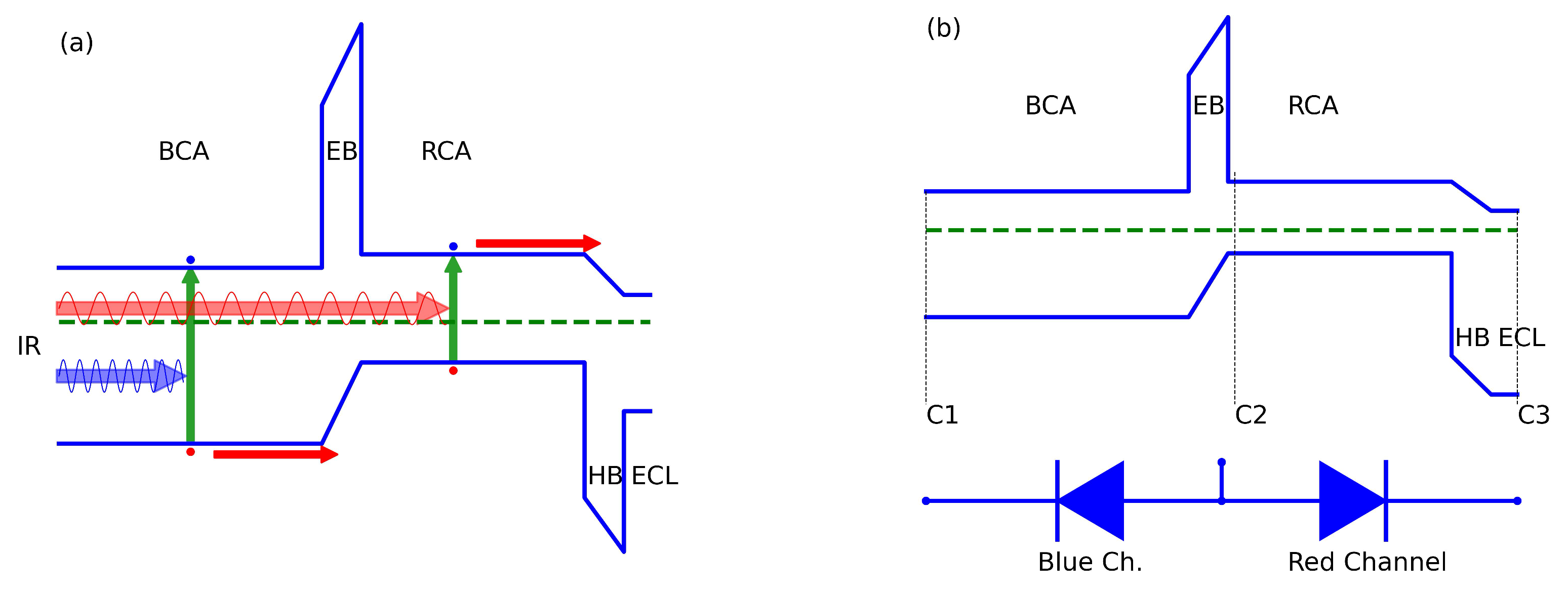
Figure 1 shows schematic energy band profiles and photogenerated carriers transport schemes with a back-to-back diode representation of the DBIRD.
As shown in
Figure 1a, IR radiation absorbed in the blue channel absorber (BCA) produces photogenerated electron-hole pairs, of which the holes may flow across the electron barrier (EB) to the p-type red channel absorber (RCA), resulting in a contribution to the BC detection signal. Similarly, IR radiation absorbed in the red channel absorber (RCA) produces photogenerated electron-hole pairs, of which the electron may flow across the hole barrier (HB) to the n-type electron collection layer (ECL), resulting in a contribution to the RC detection signal.
Figure 1b shows a similar energy band profile that has a different ECL and the contact positions. Here the BC device, n-B
n-p, may be accessed through the contacts C1 and C2, while the RC one, p-B
p-n, through C2 and C3. The terminals attached to C1 and C3 become cathodes for each channel and the one to C2 becomes a common anode. As shown in
Figure 1b, the DBIRD as a whole consists of back-to-back diodes with C2 as the common anode.
The access to one channel is independent of the other, which means that each channel of the DBIRD can be independently accessed; this is highly preferable for high-speed IR imaging applications. Each channel device may be independently biased to near zero reverse bias. Hence the DBIRD is appropriate for high-speed dual-band thermal imaging. It can also provide operational flexibility, such as variable integration times and sequential access to the two channels.
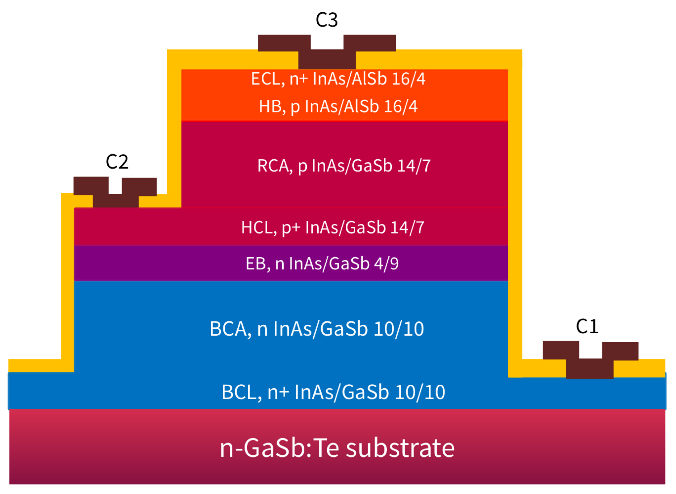
Figure 2 shows a schematic cross-sectional view of a MW/LWIR DBIRD. Each absorber layer thickness should be less than the diffusion length of the minority carrier, and longer than the absorption length, 1/
, for in-band photons in each channel with absorption coefficient
. The diffusion length of holes, the minority carrier of the BCA, may be estimated as follows:
where,
is the Boltzmann constant,
q is electron charge, and
,
,
, and
are hole diffusion length, diffusion coefficient, lifetime, and mobility, respectively. For the BCA of an InAs 10 MLs/GaSb 10 MLs T2SL with a hole mobility of 450
and hole lifetime of 100
[
3,
18], the estimated hole diffusion length is approximately 5.4
m at 77 K. The absorption length of in-band photon is about 3.3
m. So the optimal thickness of the BCA is about 5
m, producing approximately 77.6% absorption in the BCA. A low dopant concentration of each absorber is preferable in high quality materials to produce long minority carrier lifetimes.
Unipolar barrier design is the most important part of a DBIRD. It is interesting and complex. Three features in the barrier design are essential to make the device operate properly. The first is the band offsets, which are the valence band offset (VBO) in the BC, a minority hole device, and the conduction band offset (CBO) in the RC, a minority electron device. As shown in
Figure 1, the VBO between the EB and its adjacent layers should be minimized, while the CBO between the HB and its adjacent layers should likewise be minimized. The second feature is doping type and concentration of each barrier layer. The doping type of the barrier should be the same as that of the absorber to place the metallurgical junction at the position where unipolar barrier meets the signal carrier collection layer, for example the ECL and hole collection layer (HCL) on which C2 is based as shown in
Figure 2. Each barrier doping concentration should be determined to confine the depletion region within that layer. The third feature is the height of each barrier, which may affect the Shockley-Read-Hall (SRH) generation rate in the depletion layer. A good rule of thumb is to have the barrier height, namely its bandgap energy, be greater than twice the
of the absorber layer. The thickness of barrier is also important, namely to prevent the tunneling of majority carriers. The VBO and CBO may be controlled via InAs/GaSb T2SL design.
The design of each minority carrier collection layer may seem simple at first, but there are some alternatives in considering its role. As shown in
Figure 1a,b, there are two choices of the ECL material. The first is the same material as the RCA with n-type doping. Since the ECL is not involved in IR absorption but acts as an electron collector, it can be made of the same material as the barrier, such as an InAs/AlSb T2SL, but with a different doping type. This choice of ECL material gives two additional benefits: (i) ease of growth of the ECL, and (ii) a self-passivation effect with a wide
material. The choice of HCL is the RCA material with a high doping concentration for contact formation.
Table 1 presents a detailed layer design for the MW/LWIR DBIRD shown in
Figure 2.
2.2. Material Growth and Device Processing Technology
T2SLs are typically grown on GaSb (001) substrates by molecular beam epitaxy (MBE). The strengths of MBE include precise compositional control and abrupt interfaces. Solid III-V sources are employed, and Group V’s usually have valved cracking cells. The growth initiates with a GaSb buffer layer to reduce the influence of any impurities or surface defects on the substrate. This is followed by the growth of the T2SL, which is designed to have an average lattice constant matched to that of the substrate. In situ material quality monitoring during growth is often undertaken with reflection high energy electron diffraction (RHEED). Recent papers containing growth and material characterization details include references [
19,
20].
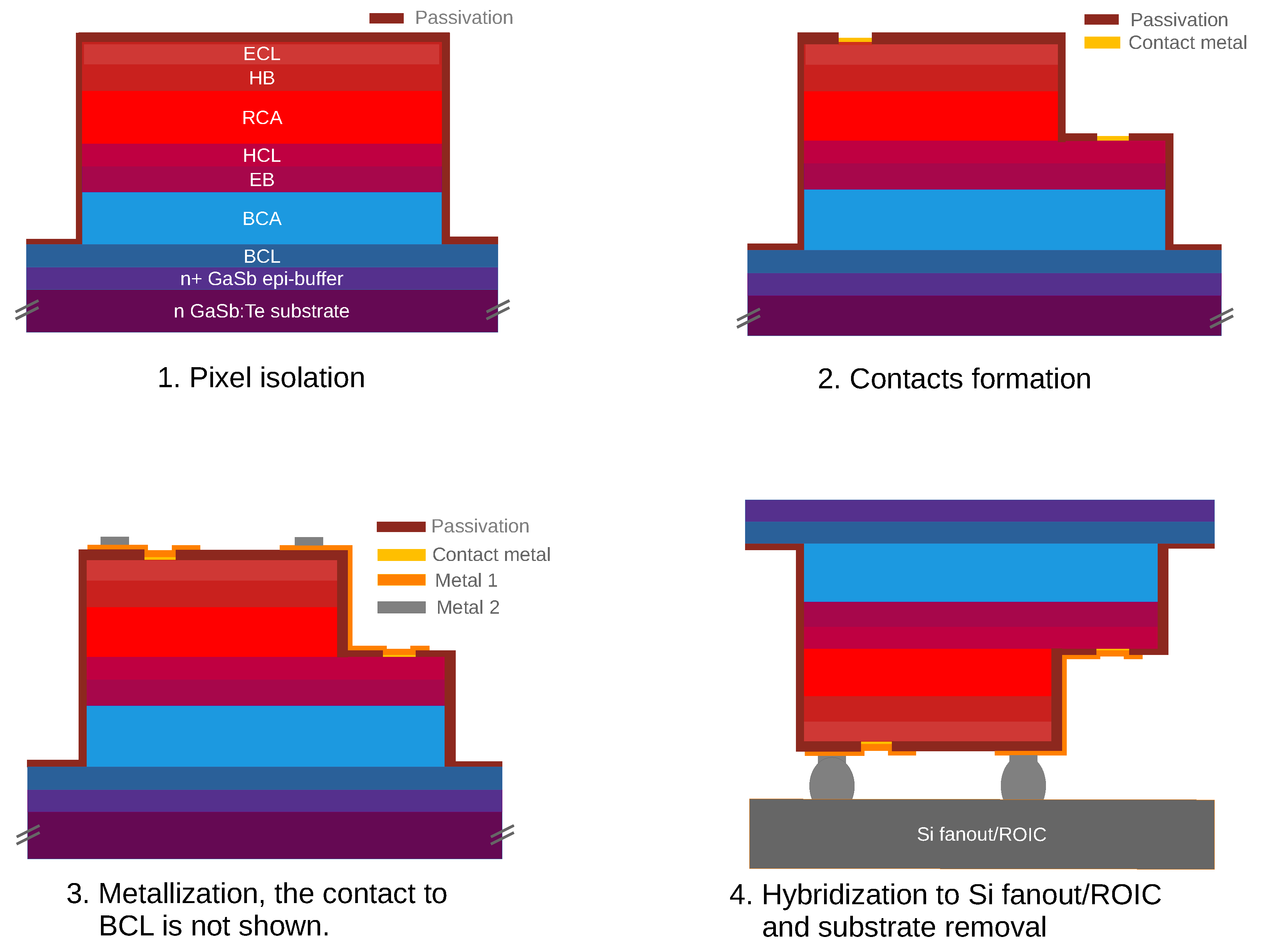
Device processing starts with an epitaxial T2SL materials. The device processing steps include passivation, meas etching, metal-semiconductor contacts formation, and metallization. Photolithography is frequently used to delineate areas on the T2SL material to selectively etch or deposit. The first step of device processing is the formation of a passivation layer to protect the T2SL materials. An additional passivation layer is necessary whenever the material surface will be exposed to air. This is followed by a deep mesa etch to achieve pixel isolation, in which the etch stop must be near the BCL as shown in
Figure 2. The next steps is forming metal-semiconductor contacts, one to the HCL and another to the ECL. A contact to the BCL is also necessary. Following are the metallization steps to make metal lines from the contacts to the bump pads, which are placed on the same level on the mesa area. After the metallization steps, the processed DBIRD chip needs to be hybridized to a Si-fanout or read-out integrated circuit to test its electro-optical properties.
Figure 3 shows schematic diagrams of selected processing steps. Recent papers describing the device processing of T2SL infrared detectors include references [
21,
22,
23,
24].
2.3. DBIRD Modeling and Simulation
To assure correct device operation and to predict the electrical and optical performance, a series of modeling efforts was undertaken on the DBIRD shown in
Figure 2. Each T2SL layer was treated as an equivalent semiconductor material having a fixed
. Then heterojunction theory was applied to calculate the CBO and VBO between adjacent layers.
Table 2 lists the employed T2SL material properties at 77 K used in this study [
3,
4,
8,
12,
25,
26,
27].
The basic semiconductor equations to be solved include Poisson’s equation coupled with the continuity equations of electrons and holes. Poisson’s equation is as follows:
where
is relative permittivity,
is the electrostatic potential, q is the elementary electron charge,
,
, and
are the concentrations of holes, electrons, ionized donors, and acceptors, respectively.
The continuity equations of electron and hole are as follows:
where
and
are the electron and hole current density,
is photogeneration rate by absorbed photons and
is the SRH recombination rate. The electron and hole current densities are as follows:
where
and
are the electron and hole mobilities,
and
are the electron and hole diffusivities.
To evaluate the spectral IR response of a DBIRD, the wavelength dependence of the absorption coefficient was obtained first. The absorption coefficients are modeled after Ref. 2, 22 as follows [
2,
28]:
where
, and
are fitting parameters with experimental data, and
. In this work,
, and
for BC,
, and
for RC, respectively, and
for both BC and RC are used.
The photogeneration rate was modeled as follows:
where
is the photogeneration rate in
is the reflectance at surface,
is the photon irradiance at
in
,
is the absorption coefficient, and
x is a position from surface. Here, the photon irradiance on to detector surface
can be expressed as the sum of two terms, one from signal source and another from cold shield, and was modeled as follows:
where
is cold shield F-number,
and
are the spectral photon radiance of blackbody source and cold-shield of detector in
. With Eq.
10, not only the spectral photon irradiance but in-band photon irradiance on to surface of detector can be evaluated. For spectral photocurrents, the photon radiance of a 500
K black-body and cold-shield
were used. Also for in-band photocurrents, the photon radiance of a 300
K black-body and no cold-shield, that is,
were used.
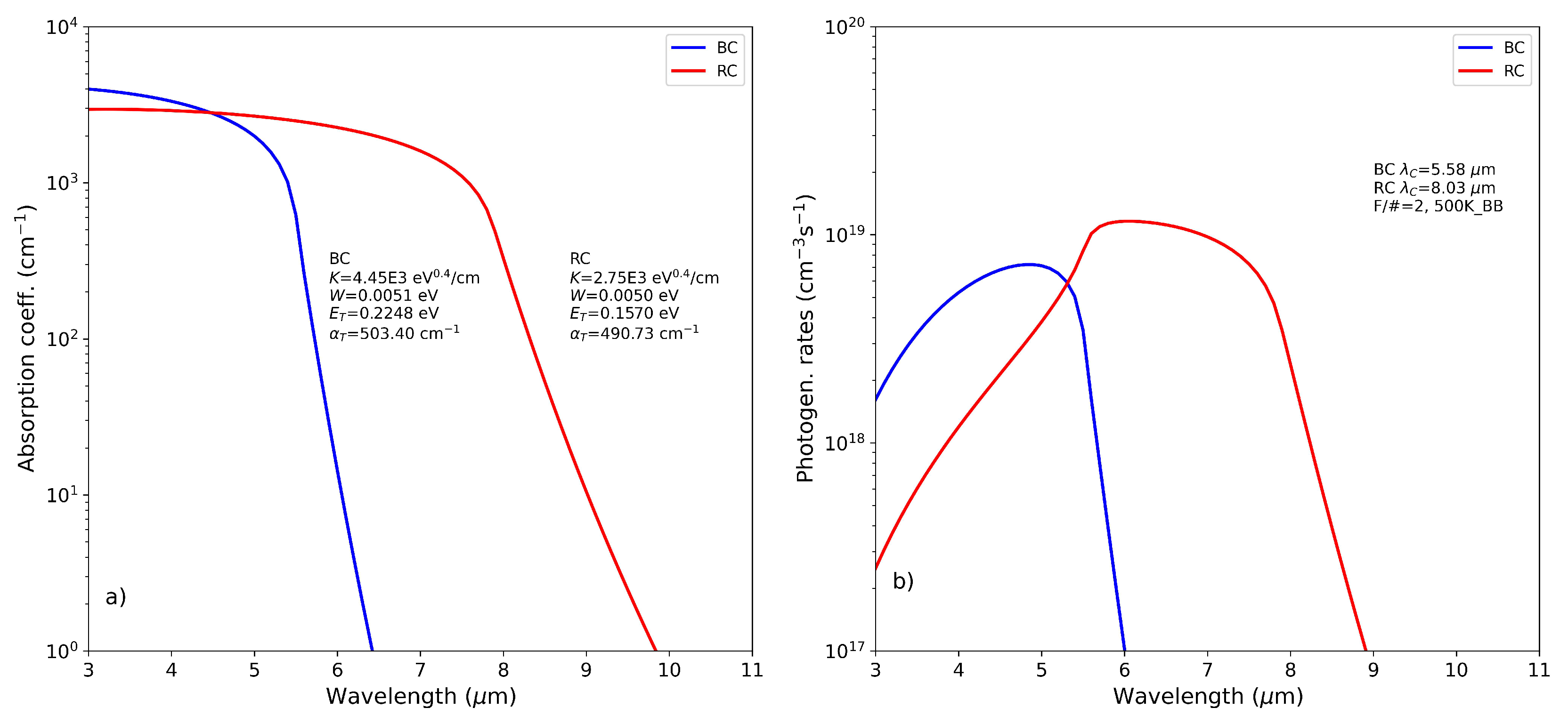
Figure 4 shows the modeling results of absorption coefficients and photogeneration rates for both BC and RC in this study. The spectral QE, responsivity, and normalized detectivity were evaluated as follows:
where
is the spectral irradiance at
,
is the quantity
X at wavelength
.
The COMSOL Multiphysics package was used to solve the basic semiconductor transport equations with and without photon illumination on the designed DBIRD. Simulations in thermal equilibrium state at 77 K were first performed with a 1-dimensional model of the DBIRD design, while simulations under bias were performed on each channel device of BC and RC. Under steady-state conditions, the parametric simulations of applied bias with and without photogeneration provided the dark current density J
dark and photocurrent density J
ph. In current density simulations, SRH generation was included with a lifetime of 100 ns and is assumed to be the limiting contributor to the dark current [
26,
27]. This assumption is thought to be valid at low bias voltages, less than 0.3 V, where generation-recombination currents through SRH recombination centers in the space charge region dominate. The J-V curves were obtained from the steady-state parametric simulations with bias voltage and photon illumination.
More detailed descriptions of the T2SL photodetector models may be found in recent published works [
2,
15,
29].
3. Results and Discussion
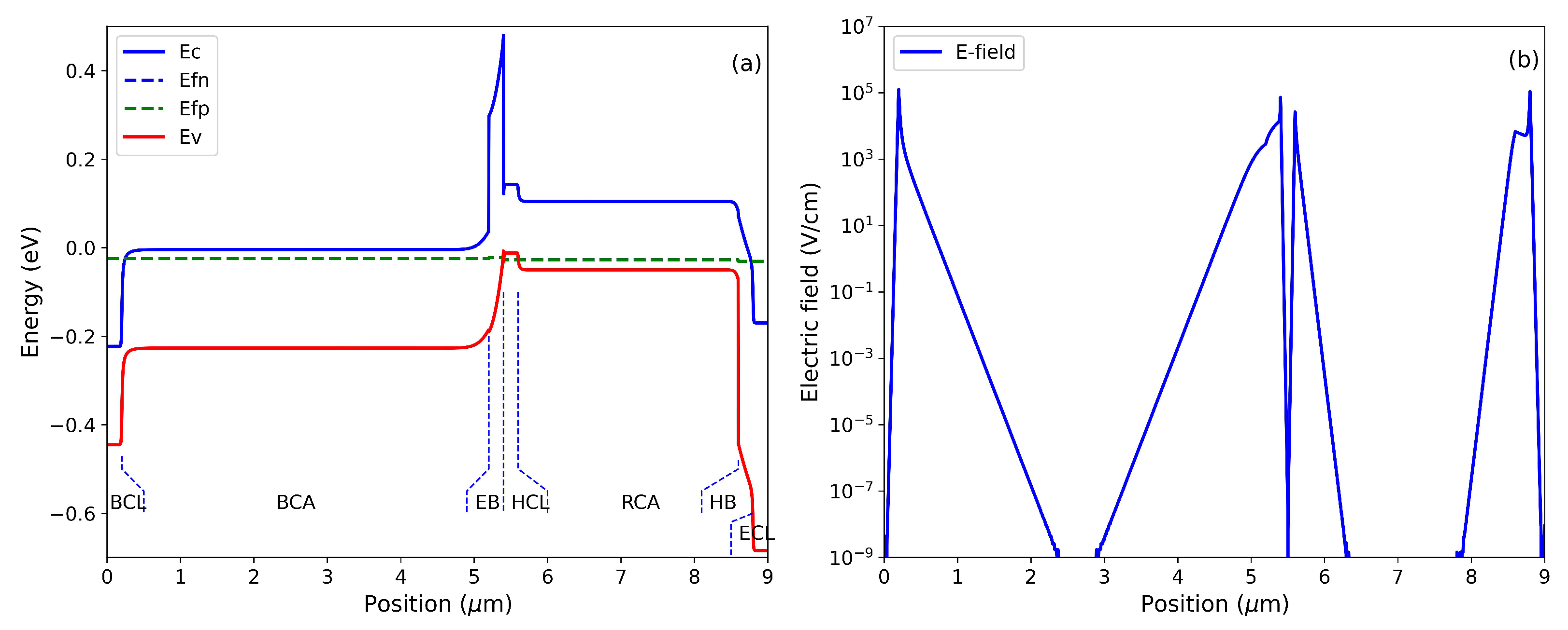
Figure 5 shows the energy band and electric field profiles of the DBIRD design in thermal equilibrium at 77 K. Other than the bottom contact layer (BCL), hole collection layer (HCL) and electron collection layer (ECL), the energy band profile in
Figure 5a) is very similar to the schematic one shown in
Figure 1. The high doping concentration layers BCL, HCL and ECL, which are necessary in a real device to make ohmic metal-semiconductor contacts, were added to produce a more realistic energy band profile. Note that there are no significant potential barriers to minority carriers in both the valence band of the BC and the conduction band of the RC, as intended, so photogenerated minority carriers in the absorber layers can move freely across the barrier to collecting layer of each channel, resulting in photocurrents at the BC and RC. The VBO between EB and BCA layer is found to be approximately 6 meV while the CBO between HB and RCA layer is found to be negative, approximately -10 meV. Specifically, the photogenerated holes, minority carriers in the BCA layer, can move freely across the barrier layer to the HCL, resulting in a BC signal current. At the same time, the photogenerated electrons, minority carriers in the RCA layer, can move freely to the ECL, resulting in a RC signal current. In
Figure 5b, note that most of the high electric field, of strength larger than about
, is almost completely confined within the barrier layers, which have a lager gap energy. This is expected to help suppress dark current and result in high performance detectors with low noise and high sensitivity.
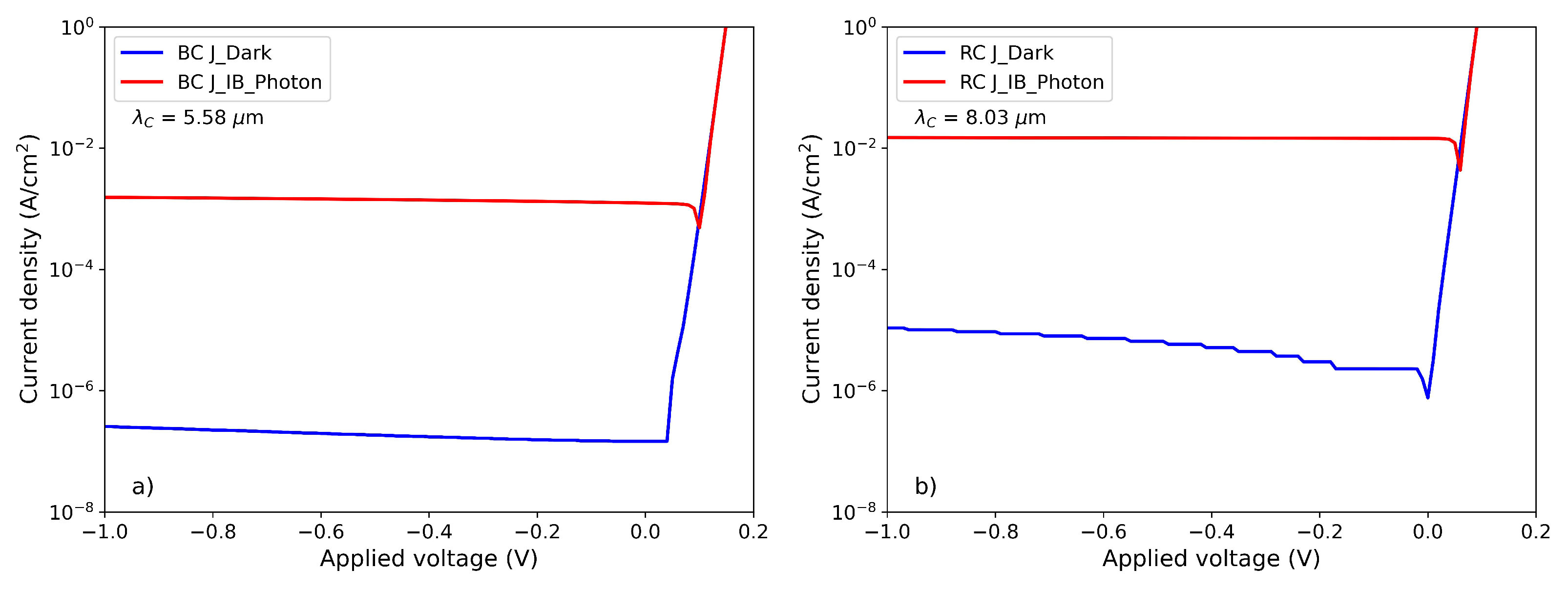
Figure 6 shows the current density-voltage (J-V) curves of the BC and RC devices of the DBIRD at 77 K; with and without incident photons. As shown in
Figure 6, the dark current of the BC is almost flat up to the reverse bias of -1 V, while that of the RC slightly increases with increasing reverse bias up to -1V. The dark currents of the BC and RC are
and
at a reverse bias of V=-0.2 V, respectively. These values are comparable with the recent published experimental results, approximately
and
at V=-0.2 V, at 80 K, respectively, in an NBn dual-band IR detector [
30]. Considering also that the theoretically estimated dark current density of T2SL InAs/GaSb nBn at 77 K are less than
for
and
for
, respectively [
31], the dark current of DBIRD seems to be as good as from a well passivated T2SL InAs/GaSb single color nBn device. Photoresponses may be evaluated from the photocurrents under photon irradiance
. The QE, responsivity and
of the BC are evaluated as 28%, 1.12 A/W and
at -0.2 V reverse bias, while those of the RC are 32%, 1.87 A/W and
. The J-V curves together with the energy band and the electric field profile in
Figure 5 strongly suggest that the DBIRD operates as a dual-band detector as designed. In addition, the dark current levels are reasonable in comparison with experimental results from devices with the same [
30,
32] and similar materials [
14,
26].
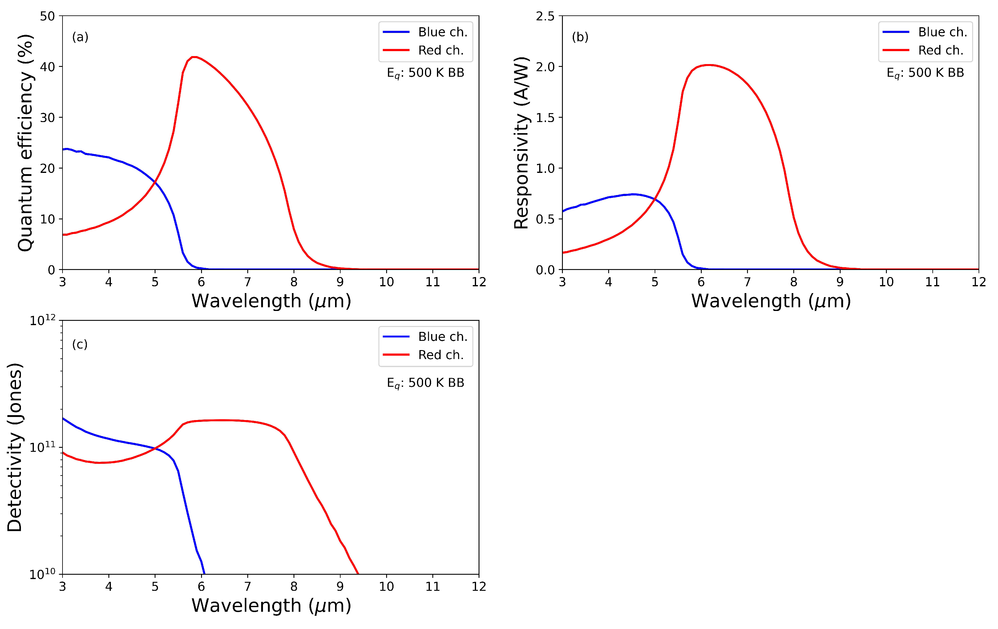
Figure 7 shows the spectral QE, responsivity. and normalized detectivity of the two channels in the DBIRD. The spectral photoresponse were evaluated from the photocurrent density at -0.2 V reverse bias. The QE of the BC decreases with increasing wavelength from 23.6% at 3
, while that of the RC has a peak of 42.1% at 5.8
. These values of QE are comparable with previous studies [
14,
26,
32]. The responsivity of the BC has its peak of 0.74
at 4.5
, while that of the RC has its peak of 2.02
at 6.2
.
Figure 7 also shows that the normalized detectivity of the BC is
at 3
, and decreases as wavelength increases, while that of RC has a peak value of
at 6.5
. Note that these values are fairly high in comparison with in-band ones.
The low QE of the BC is due to the BCA’s low absorption coefficient, which results in relatively large spectral crosstalk of the RC. The unabsorbed blue band photons in the BCA are transmitted to the RCA and absorbed, increasing crosstalk of the RC to photons in the BC wavelength range. IR absorption in the BCA will increase with increasing absorber thickness to a certain extent. To increase QE by increasing IR absorption, the IR absorbing layer thickness should be increased within its minority carrier diffusion length. In our BC device, the absorbing layer thickness was chosen to be its maximum values, which is less than the minority carrier hole diffusion length.
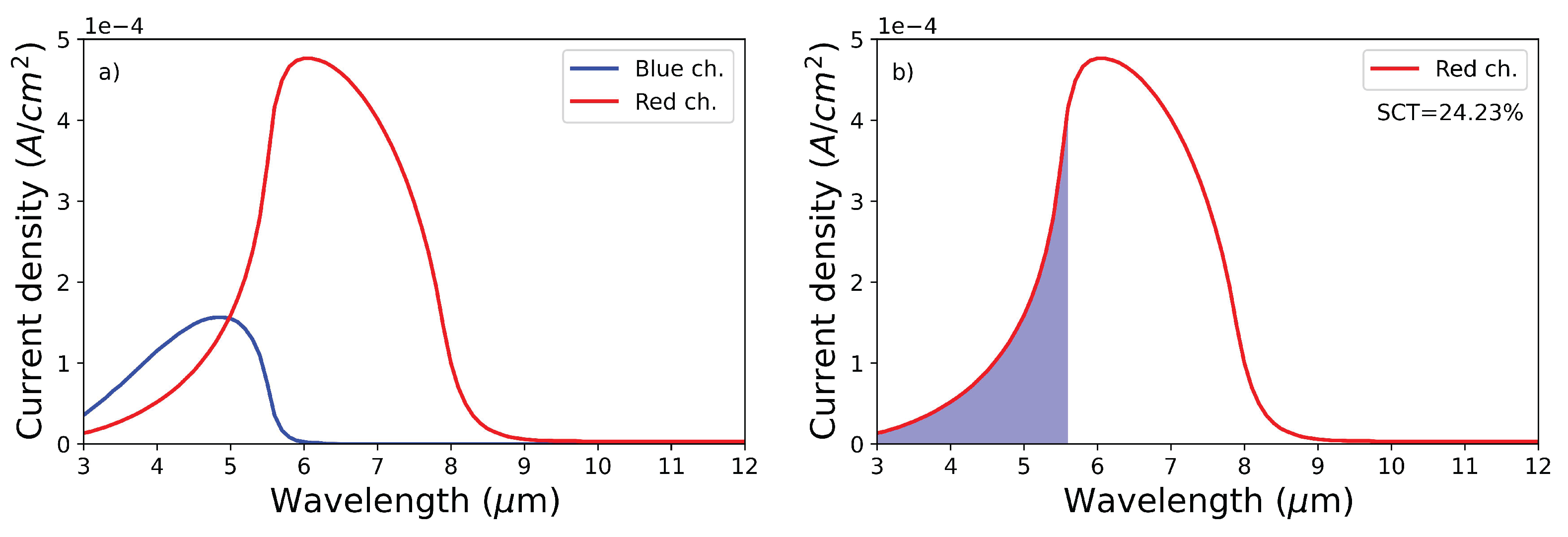
Figure 8 shows the spectral photocurrent densities of the two channels and the cross-talk of the RC in the DBIRD. The spectral cross-talk of the RC in the blue band is defined as the ratio of photocurrent generated by absorbing residual blue band IR in RCA,
to the total photocurrent generated by the RC
[
2],
The photocurrents,
and
can be evaluated by integrating the spectral photocurrent curve of the RC. As shown in
Figure 8,
is the area of shaded region over
, while
is the total area under the spectral current density curve of the RC.
The evaluated spectral crosstalk of the RC in blue band may be 24.23%. This suggests 24.23% of the RC photocurrent under illumination with a 500 K blackbody may come from the contributions from the blue band. This value is high in comparison with that in the same dual-band detector using HgCdTe.
4. Conclusions
We have reported a novel dual-band barrier IR detector using InAs/GaSb T2SLs, named DBIRD. The structure of the DBIRD is nBpBn. It utilizes unipolar barriers to make each channel independently accessible, and to suppress generation-recombination current in the space charge region of each channel. A specific DBIRD has been designed and explored. Device modeling and the estimation of dark current and photocurrents were carried out. The estimated performance suggests that the DBIRD will perform as a dual-band detector per design. The performance of the DBIRD shows low dark currents in each channel device, in-band QE of 28% in the BC and 32% in the RC, and spectral QE of 23.6% in the BC and 42.1% at its peak in the RC. The DBIRD may provide a significantly improved capability and operational flexibility for high-speed dual-band imaging in comparison with NBn dual-band detectors.
Author Contributions
Conceptualization, S.P. and C.G.; methodology, S.P. and C.G.; software, S.P.; validation, S.P. and C.G.; formal analysis, S.P. and C.G.; investigation, S.P.; resources, S.P.; data curation, S.P.; writing—original draft preparation, S.P. and C.G.; writing—review and editing, S.P. and C.G.; visualization, S.P. and C.G. All authors have read and agreed to the published version of the manuscript.
Institutional Review Board Statement
Not applicable.
Informed Consent Statement
Not applicable.
Data Availability Statement
All data generated and analyzed during this study are included in this published article.
Conflicts of Interest
The authors declare no conflicts of interest.
Abbreviations
The following abbreviations are used in this manuscript:
| DBIRD |
Dual-band Barrier IR Detector |
| T2SLs |
Type-II Superlattices |
| BC, RC |
Blue, Red Channel |
| HJs |
Heterojunctions |
| VBO |
Valence Band Offset |
| CBO |
Conduction Band Offset |
| MW/LW |
Middle and long wavelength |
| BCA |
Blue Channel Absorber |
| RCA |
Red Channel Absorber |
| EB |
Electron Barrier |
| HB |
Hole Barrier |
| ECL |
Electron Collection Layer |
| HCL |
Hole Collection Layer |
| SRH |
Shockley-Read-Hall |
| QE |
Quantum Efficiency |
| SCT |
Spectral Cross-talk |
References
- Haddadi, A.; Dehzangi, A.; Chevallier, R.; Adhikary, S.; Razeghi, M. Bias–selectable nBn dual–band long–/very long–wavelength infrared photodetectors based on InAs/InAs1-xSbx/AlAs1-xSbx type–II superlattices. Sci. Rep. 2017, 7, 1–7. [Google Scholar] [CrossRef]
- Ariyawansa, G.; Grupen, M.; Duran, J.M.; Scheihing, J.E.; Nelson, T.R.; Eismann, M.T. Design and modeling of InAs/GaSb type II superlattice based dual-band infrared detectors. Journal of Applied Physics 2012, 111, 073107. [Google Scholar] [CrossRef]
- Plis, E.; Myers, S.; Ramirez, D.; Smith, E.; Rhiger, D.; Chen, C.; Phillips, J.; Krishna, S. Dual color longwave InAs/GaSb type-II strained layer superlattice detectors. Infrared Physics & Technology 2015, 70, 93–98. [Google Scholar] [CrossRef]
- Razeghi, M.; Dehzangi, A.; Li, J. Multi-band SWIR-MWIR-LWIR Type-II superlattice based infrared photodetector. Results in Optics 2021, 2, 100054. [Google Scholar] [CrossRef]
- Blazejewski, E.R.; Arias, J.M.; Williams, G.M.; McLevige, W.; Zandian, M.; Pasko, J. Bias-switchable dual-band HgCdTe infrared photodetector. Journal of Vacuum Science & Technology B: Microelectronics and Nanometer Structures Processing, Measurement, and Phenomena 1992, 10, 1626–1632. [Google Scholar] [CrossRef]
- Reine, M.; Norton, P.; Starr, R.; Weiler, M.H.; Kestigian, M.; Musicant, B.L.; Mitra, P.; Schimert, T.; Case, F.C.; Bhat, L.; Ehsani, H.; Rao, V. Independently accessed back-to-back HgCdTe hotodiodes: A new dual-band infrared detector. Journal of Electronic Materials 1995, 24, 669–679. [Google Scholar] [CrossRef]
- Kopytko, M.; Gawron, W.; Kębłowski, A.; Stępień, D.; Martyniuk, P.; Jóźwikowski, K. Numerical analysis of HgCdTe dual-band infrared detector. Optical and Quantum Electronics 2019, 51. [Google Scholar] [CrossRef]
- Klipstein, P.C.; Livneh, Y.; Glozman, A.; Grossman, S.; Klin, O.; Snapi, N.; Weiss, E. Modeling InAs/GaSb and InAs/InAsSb Superlattice Infrared Detectors. Journal of Electronic Materials 2014, 43, 2984–2990. [Google Scholar] [CrossRef]
- Gautam, N.; Myers, S.; Barve, A.V.; Klein, B.; Smith, E.P.; Rhiger, D.R.; Kim, H.S.; Tian, Z.B.; Krishna, S. Barrier Engineered Infrared Photodetectors Based on Type-II InAs/GaSb Strained Layer Superlattices. IEEE Journal of Quantum Electronics 2013, 49, 211–217. [Google Scholar] [CrossRef]
- Ariyawansa, G.; Perera, A.G.U.; Huang, G.; Bhattacharya, P. Wavelength agile superlattice quantum dot infrared photodetector. Applied Physics Letters 2009, 94, 131109. [Google Scholar] [CrossRef]
- Maimon, S.; Wicks, G.W. nBn detector, an infrared detector with reduced dark current and higher operating temperature. Applied Physics Letters 2006, 89, 151109. [Google Scholar] [CrossRef]
- Ting, D.Z.Y.; Hill, C.J.; Soibel, A.; Keo, S.A.; Mumolo, J.M.; Nguyen, J.; Gunapala, S.D. A high-performance long wavelength superlattice complementary barrier infrared detector. Applied Physics Letters 2009, 95, 023508. [Google Scholar] [CrossRef]
- Martyniuk, P.; Kopytko, M.; Rogalski, A. Barrier infrared detectors. Opto-Electronics Review 2014, 22, 127–146. [Google Scholar] [CrossRef]
- Wróbel, J.; Martyniuk, P.; Plis, E.; Madejczyk, P.; Gawron, W.; Krishna, S.; Rogalski, A. Dark current modeling of MWIR type-II superlattice detectors. Infrared Technology and Applications XXXVIII; Andresen, B.F.; Fulop, G.F.; Norton, P.R., Eds. International Society for Optics and Photonics, SPIE, 2012, Vol. 8353, p. 835316. [CrossRef]
- Wróbel, J.; Plis, E.; Gawron, W.; Motyka, M.; Martyniuk, P.; Madejczyk, P.; Kowalewski, A.; Dyksik, M.; Misiewicz, J.; Krishna, S.; Rogalski, A. Analysis of temperature dependence of dark current mechanisms in mid-wavelength infrared pin type-II superlattice pho- todiodes. Sensors and Materials 2014, 26, 235–244. [Google Scholar]
- Rehm, R.; Walther, M.; Rutz, F.; Schmitz, Johannes annd Wörl, A.; Masur, J.M.; Scheibner, R.; Wendler, J.; Ziegler, J. Dual-Color InAs/GaSb Superlattice Focal-Plane Array Technology. Journal of Electronic Materials 2011, 40, 1738–1743. [Google Scholar] [CrossRef]
- Rehm, R.; Walther, M.; Schmitz, J.; Wauro, M.; Luppold, W.; Niemasz, J.; Rutz, F.; Wörl, A.; Masur, J.M.; Kirste, L.; Scheibner, R.; Wendler, J.; Ziegler, J. Substrate removal of dual-colour InAs/GaSb superlattice focal plane arrays. physica status solidi c 2012, 9, 318–321. [Google Scholar] [CrossRef]
- Rehm, R.; Masur, M.; Schmitz, J.; Daumer, V.; Niemasz, J.; Vandervelde, T.; DeMeo, D.; Luppold, W.; Wauro, M.; Wörl, A.; Rutz, F.; Scheibner, R.; Ziegler, J.; Walther, M. InAs/GaSb superlattice infrared detectors. Infrared Physics & Technology 2013, 59, 6–11. [Google Scholar] [CrossRef]
- Xu, Z.; Chen, J.;Wang, F.; Zhou, Y.; Bai, Z.; Xu, J.; Xu, Q.; Jin, C.; He, L. MBE growth and characterization of type-II InAs/GaSb superlattices LWIR materials and photodetectors with barrier structures. Journal of Crystal Growth 2017, 477, 277–282. Proceeding of the 19th International Conference on Molecular Beam Epitaxy. [CrossRef]
- Jasik, A.; Sankowska, I.; Regiński, K.; Machowska-Podsiadło, E.; Wawro, A.; Wzorek, M.; Kruszka, R.; Jakieła, R.; Kubacka-Traczyk, J.; Motyka, M.; others. MBE growth of type II InAs/GaSb superlattices on GaSb buffer. Crystal growth: theory, mechanisms and morphology 2012.
- Alchaar, R.; Rodriguez, J.B.; Höglund, L.; Naureen, S.; Christol, P. Characterization of an InAs/GaSb type-II superlattice barrier photodetector operating in the LWIR domain. AIP Advances 2019, 9, 055012. [Google Scholar] [CrossRef]
- Chaghi, R.; Cervera, C.; Aït-Kaci, H.; Grech, P.; Rodriguez, J.B.; Christol, P. Wet etching and chemical polishing of InAs/GaSb superlattice photodiodes. Semiconductor Science and Technology 2009, 24, 065010. [Google Scholar] [CrossRef]
- Bouschet, M.; Zavala-Moran, U.; Arounassalame, V.; Alchaar, R.; Bataillon, C.; Ribet-Mohamed, I.; de Anda-Salazar, F.; Perez, J.P.; Péré-Laperne, N.; Christol, P. Influence of Pixel Etching on Electrical and Electro-Optical Performances of a Ga-Free InAs/InAsSb T2SL Barrier Photodetector for Mid-Wave Infrared Imaging. Photonics 2021, 8. [Google Scholar] [CrossRef]
- Lee, H.J.; Eom, J.H.; Jung, H.C.; Kang, K.K.; Ryu, S.M.; Jang, A.; Kim, J.G.; Kim, Y.H.; Jung, H.; Kim, S.H.; others. Design and performance of dual-band MWIR/LWIR focal plane arrays based on a type-II superlattice nBn structure. Opto-Electronics Review 2023, 31. [Google Scholar]
- Dente, G.C.; Tilton, M.L. Comparing pseudopotential predictions for InAs/GaSb superlattices. Phys. Rev. B 2002, 66, 165307. [Google Scholar] [CrossRef]
- Martyniuk, P.; Wróbel, J.; Plis, E.; Madejczyk, P.; Kowalewski, A.; Gawron, W.; Krishna, S.; Rogalski, A. Performance modeling of MWIR InAs/GaSb/B–Al0.2Ga0.8Sb type-II superlattice nBn detector. Semiconductor Science and Technology 2012, 27, 055002. [Google Scholar] [CrossRef]
- Delmas, M.; Rodriguez, J.B.; Christol, P. Electrical modeling of InAs/GaSb superlattice mid-wavelength infrared pin photodiode to analyze experimental dark current characteristics. Journal of Applied Physics 2014, 116, 113101. [Google Scholar] [CrossRef]
- Moazzami, K.; Phillips, J.; Lee, D.; Krishnamurthy, S.; Benoit, G.; Fink, Y.; Tiwald, T. Detailed study of above bandgap optical absorption in HgCdTe. Journal of Electronic Materials 2005, 34, 773–778. [Google Scholar] [CrossRef]
- Asplund, C.; Marcks von Würtemberg, R.; Höglund, L. Modeling tools for design of type-II superlattice photodetectors. Infrared Physics & Technology 2017, 84, 21–27. [Google Scholar] [CrossRef]
- Lee, H.J.; Eom, J.H.; Jung, H.C.; Kang, K.K.; Ryu, S.M.; Jang, A.; Kim, J.G.; Kim, Y.H.; Jung, H.; Kim, S.H.; et al.. Design and performance of dual-band MWIR/LWIR focal plane arrays based on a type-II superlattice nBn structure. Opto-Electronics Review 2023, Vol. 31, Special Issue, art. no. e144560. [CrossRef]
- Rogalski, A.; Kopytko, M.; Martyniuk, P. Antimonide-based Infrared Detectors: A New Perspective; SPIE press: Boston, 2018; pp. 166–179. [Google Scholar] [CrossRef]
- Li, Y.; Xiao, W.; Wu, L.; Xie, X.; Lu, P.; Wang, S. Dark Current Characteristic of p-i-n and nBn MWIR InAs/GaSb Superlattice Infrared Detectors. 2019 IEEE 4th Optoelectronics Global Conference (OGC), 2019, pp. 70–75. [CrossRef]
|
Disclaimer/Publisher’s Note: The statements, opinions and data contained in all publications are solely those of the individual author(s) and contributor(s) and not of MDPI and/or the editor(s). MDPI and/or the editor(s) disclaim responsibility for any injury to people or property resulting from any ideas, methods, instructions or products referred to in the content. |
© 2024 by the authors. Licensee MDPI, Basel, Switzerland. This article is an open access article distributed under the terms and conditions of the Creative Commons Attribution (CC BY) license (https://creativecommons.org/licenses/by/4.0/).
