Preprint
Article

Elemental Dissolution in Multicomponent PDC Based Mixed-Phase Hard Films

Altmetrics

Downloads

103

Views

20

Comments

0

This version is not peer-reviewed

Submitted:

07 April 2024

Posted:

08 April 2024

You are already at the latest version

Alerts
Abstract
Due to the high temperature limitation associated with silicon, SiC, Si3N4, TiC, TiN, TiB2, cBN, CNx, SiO2, Al2O3 and novel multicomponent nanocomposites polymer derived ceramics (PDC) based thin films like Si-C-N, Ti-Si-B-C-N and Si-O-CN that are compatible with silicon and have a wider range of operation in ambient conditions are being investigated. Apart from small scale electro-mechanical devices like N/MEMS, sensors, areas like metallurgical protection, water purification, energy storage, bio medical implants and aerospace have been benefited. The cross-sectional study involving the role of oxygen and nitrogen dissolution at different interfacial configurations has been presented.
Keywords: 
Subject: Engineering  -   Metallurgy and Metallurgical Engineering

1. Introduction

Nanoindentation is one of the most coveted mechanical characterization techniques at nanoscale for various types of materials which includes, alloys, nanomaterials, and thin films [1,2,3,4] The loading parameters which include load, depth, strain-rate, indenter shape, holding time etc leaves an impact pertaining to which the choice of material for specific low dimensional application can be envisaged [5,6,7] They are being merged with microscopic techniques (AFM) and are being applied on unconventional materials like conducting polymers, bio ceramics and human bones and tissue [8,9,10].
Multicomponent materials like high-entropy alloys (HEA) and high-entropy ceramics (HEC) on the other hand have surface out in recent times as significant materials having vast technological importance. High Entropy Alloy (HEA) is a composition of multiple principal elements in an equimolar or near equimolar ratio. Where the number of elements is not less than five (≥5) and the atomic % of each element between 5% and 35 %. [11,12,13]. HEAs show enhanced properties of hardness, strength, wear resistance, corrosion resistance, fatigue, and fracture resistance [14].. The mechanical properties of HEAs like yield stress, tensile strength, hardness, fracture toughness and wear resistance are significant aspects for their application and have been subject to nanoindentation [15,16]. HEAs like Co1.5CeFeNi1.5Ti, Al0.2Co1.5CrFeNi1.5Ti; AlCoCrFeNi, NbMoTaV, Cu0.5NiAlCoCrFeSi, CoCrFeNi, CoCrFeMnNi, FeCoNi, CrFeCoNi along with HEA carbides, HEA oxides, HEA carbonitrides have shown high wear resistance, tensile strength, yield strength, ductility, and fracture toughness [17,18,19,20].
Interestingly, the Polymer-derived ceramics (PDC) like Si-C-N, Si-B-C-N with enormous high temperature stability due t0 the formation of nanocomposites is being investigated over the past 30 years and fall in the category of moderate entropy alloy or ceramics (HEA/HEC) [20]. The ternary nanocomposite material Si-C-N was first introduced to the scientific community as a high-temperature oxidation-resistant polymer-derived ceramic (PDC) [21]. PDCs combine the functional properties of polymers with the mechanical and chemical durability of ceramics. Polymer-derived ceramics (PDCs) have a polymer-like nanostructure and ceramic-like properties, e.g., creep and oxidation resistance [22].
The Si-C-N has shown stability up to 1600°C and it remains in the amorphous state up to 1500oC. These properties make silicon carbonitride a promising material for prospective applications such as structural ceramics, MEMS, hard protective coatings, and electronic materials [23]. Si-C-N is being currently looked for the absorption of electromagnetic waves (shielding) [24,25,26,27], as thin film pressure and temperature sensors [28,29,30,31], as a bonding layer for memory devices [32] MEMS magnetic devices [33] and even in endodontics [34]. It has also been reported to show both metallic and piezoelectric properties and is a good alternative to SiC which only has insulating properties [35,36,37,38,39]. There have been several investigations on PDC coatings and derivatives of Si-C-N over recent years some of which are given in Table 1.
The free carbon content within the SiCN is the main factor in its performance. It affects the crystallinity affecting the mechanical properties like hardness, modulus, and fracture toughness, and the thermal and electrical conductivity which are essential properties for the use as sensors and other MEMS devices [51,52,53,58]. Theoretical calculations have been performed on the high hardness shown by Si-C-N showing the effect of high-density carbon allotropes [59] and experimental evidence of stable SiC2N2-Si2CN4 phases has also been reported recently [60] An attempt has therefore been made in this communication to investigate the role of the excess carbon in the creating the surface morphology at different deposition conditions. Although similar work has been reported by us previously [61,62,63,64], the primary focus here is on the effect of deposition pressure. The ITO/PDC thin film exhibits excellent stability, and has been reported to be using for high temperature sensing applications [65].
PDC based hard coatings are being deposited along with other multicomponent counterparts like Ti-B-N, Ti-B-Si-C(N) etc possessing mixture of nanocrystalline carbides (SiC, TiC), boride (TiB2) and nitrides (Si3N4, CNx, TiN, cBN)) phases which gives toughens them apart from providing hardness, being the necessary and sufficient properties especially for the protection of the underlying substrate [66] and has also been used in asses any intermetallic formation useful for micro electronic packaging [67]

2. Materials and Methods

The coatings deposited by magnetron sputtering (HINHIVAC, Bangalore) using sintered targets of SiC, TiB2 along with the passage of Nitrogen gas (N2) as per the requirement of the coating composition. Transmission electron microscope (EM 200, Philips) was used for morphological analysis and the mechanical characterizations were done with the help of nanoindentation (MTS USA) and scratch tester (Ducom, Bangalore)

3. Results and Discussions

The surface of the heterogeneous microstructure in the case of inhomogeneous crystallite growth is depicted in the TEM image of Si-C-N coatings, which shows the deposition of 5 nm-sized crystallites in the amorphous Si-C-N matrix deposited at 100 oC. (Figure 1a) [68] The amorphous character was amply demonstrated by the SAED pattern. When amorphous carbon (a-C) joined forces with Si and N to form an a-Si-C-N matrix, the nucleation and development of nano crystallites of β-Si3N4, β-SiC, and even nanocrystalline (nc) graphite initially started to happen. The surface profile of the designated areas showed the distribution of the nanocrystallites.
An expanded view of the amorphous region showing the formation of ultrafine crystallites is shown in Figure 1b. Using the surface profile, an approximate surface density of 0.045 nm2 was determined. Two significant peaks, each made up of smaller peaks, were visible in the linear profile. This illustrates how larger crystallites have been formed through the joining of smaller crystallites. For fracture analysis, the crystalline morphology is crucial. Greater toughness is typically provided by smaller crystallites. On the other hand, a material that is overly hard is brittle and prone to shattering. When connecting mechanical qualities to interfacial crystallinity, hard coatings need to be considered. Under ideal circumstances, the films were found to be on average harder than 20 GPa [61,62,63,69]. To investigate the stress distribution beneath the depression that causes fracture, finite element analysis was performed [70,71,72,73,74,75].
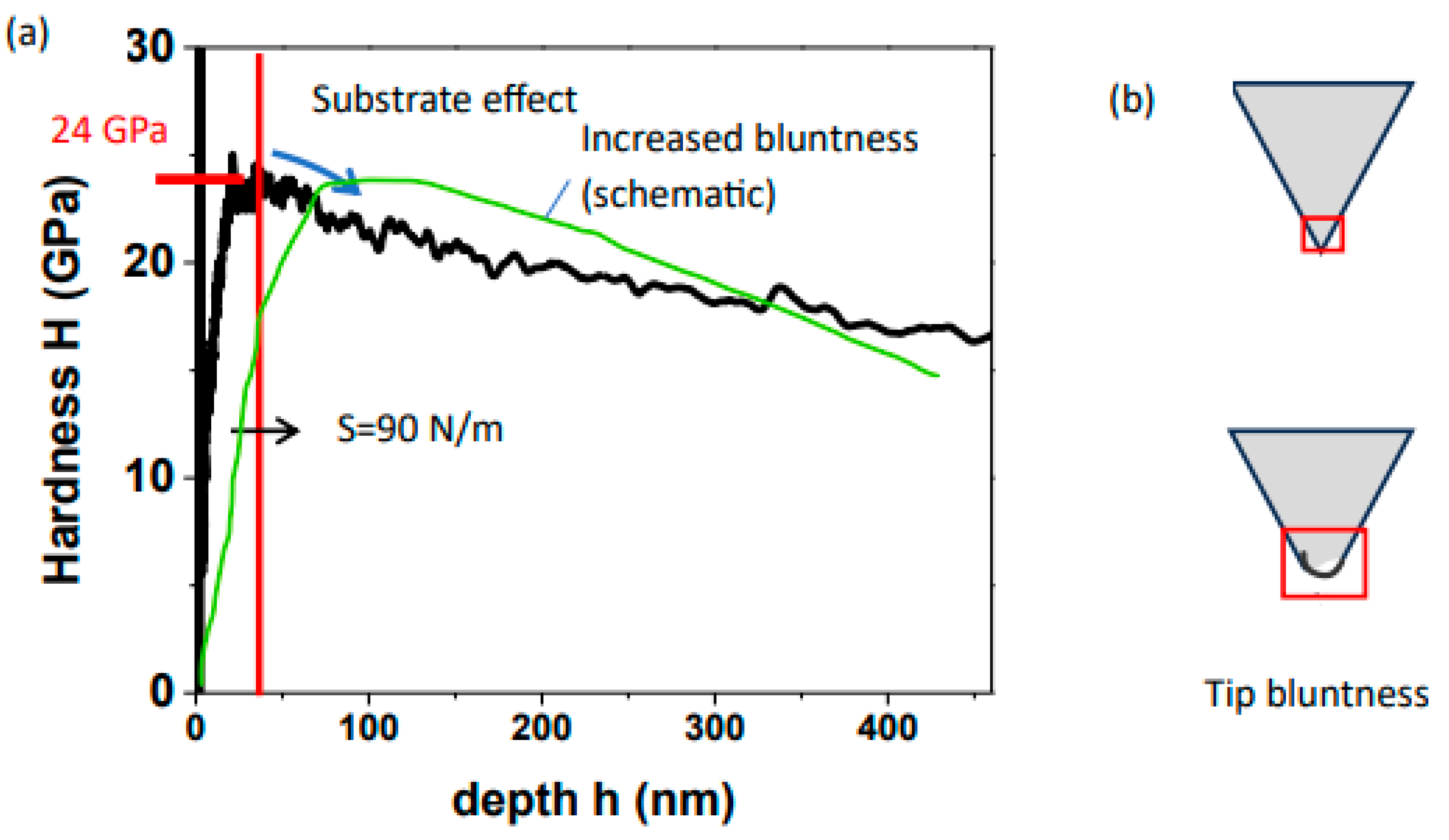
Following a predetermined depth interval, a hardness value is obtained in accordance with the initial instrumentation parameters, providing a hardness profile with depth as opposed to a single numerical value. (Figure 2a). The profile can be seen to reach a maximum followed a decrease. The maximum value is taken as the hardness which in this case is 24 GPa [61,62,63]. The substrate effect, which begins at roughly 10% of the coating thickness, is what is causing the drop. The coating appears to be roughly 400 nm thick based on the commencing at 40 nm. After being used a lot, the indenter tip needs to be adjusted since it becomes blunt and might cause the substrate effect to occur at greater stresses, as schematically shown. (Figure 2b),
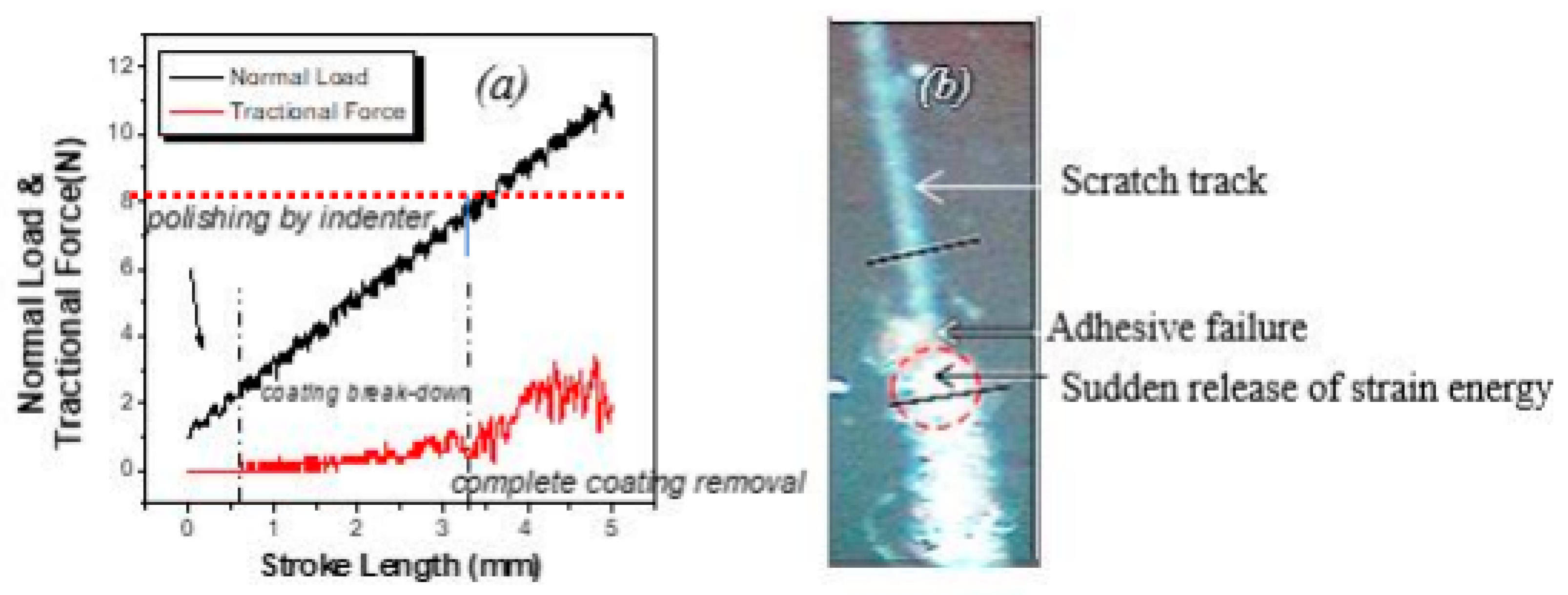
The area under the H-d plot up to 40 nm is around 90 N/m, which corresponds to the coating stiffness. The yielding generated by the Berkovich indenter is constrained till 40 nm till the substrate effect commences, which suggests the strain imposed during indentation has a deeper influence than the depth and activates the substrate effect on reaching the coating-substrate contact. SiCN's crystallographic orientation is pseudohexagonal ion (lower symmetry than standard crystallographic orientation), hence compliance components for the various normal and shear components exist. However, due to the fine crystallite size, the directional effect averages out, leaving us with a more isotropic situation. The dislocation glide observed in typical metals and alloys is difficult to achieve in these high temperature ceramics. Even at high temperatures, an increase in load applied frequently results in fracture. The interface (adhesion) therefore plays a crucial function. The adhesive characteristics of Si-C-N coatings were thoroughly explored utilising sliding indentations. The representative scratch test performed on SiCN/glass is shown in Figure 3 [76], where the coating can be seen to fail due to the release of strain energy which manifests itself by a change in the reactional force plot on being subject to a ramping sliding load. Scratch tests have also been performed on energy based smart materials, AF4 coatings on silicon (Si) and glass (SiO2) for electronic packaging, and alumina-silica coatings used in bio-medical implants [77,78].
High entropy alloys (HEA) and high entropy ceramics (HEC) are examples of multicomponent materials that are currently being studied, as was indicated in the introductory section. Similar to this, as time has gone on, more elemental species have been added to tertiary, quaternary, and quinary nanocomposites. The material Ti-B-Si-C has been deposited as nanocomposite coatings utilising either a single target of Ti-B-Si-C or two distinct targets of TiB2 and SiC. The presence of TiB2 has primarily contributed to the material's hardness exceeding 40 GPa. Ti-B-Si-C has a better fracture toughness than other binary or ternary nanocomposite materials. The dislocation distribution in front of a developing fracture was linked to the fractographic features [79]
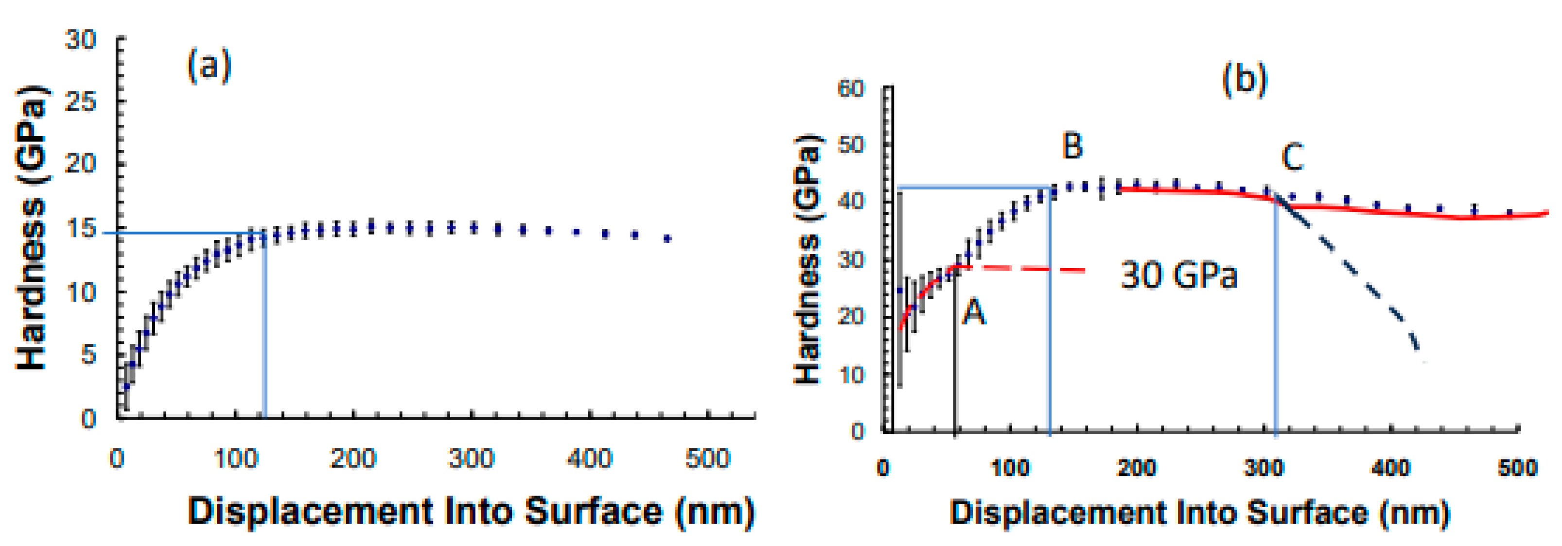
Nitrogen incorporation along will lead to formation of tertiary Ti-B-N or quinary Ti-B-Si-C-N nanocomposite coatings having constituent phases formed asper the deposition conditions employed. The difficulty however one faces is the loss of control on the tune ability of the different possibility phases as the component number enhances. A decrease in hardness was found with the addition nitrogen further to Ti-B-Si-C implying the fact that it was due to TiB2 and/or TiC which was providing the high values of hardness and nitrogen incorporation probably caused the deposition of Si-C-N based phases which usually have a higher fraction of amorphization and have greater chances of graphitization due to the excess carbon present in the structure [20] with a comparatively reduced hardness (Figure 4a,b).
Another observation made from the hardness profile is that it can be deconvoluted into two separate profiles as shown with 30 GPa profile region A) getting merged at around 50nm with the finally obtained 40GPa profile (regio B). A shift of the 40GPa profile to lower values takes place around 320nm (region C) which may not be the usual substrate effect as the curve does not follow a continuous decrease as shown by the dotted line. A possible explanation of the above observations is in the formation of multi-phased composition which shows a cross sectional variation, an effect which became prolific due to nitrogen. In case of multilayers, an alternate harder and softer coatings pin the dislocations at the interface restricting their motion making the coatings hard not at the expense of losing the toughness to a significant amount.
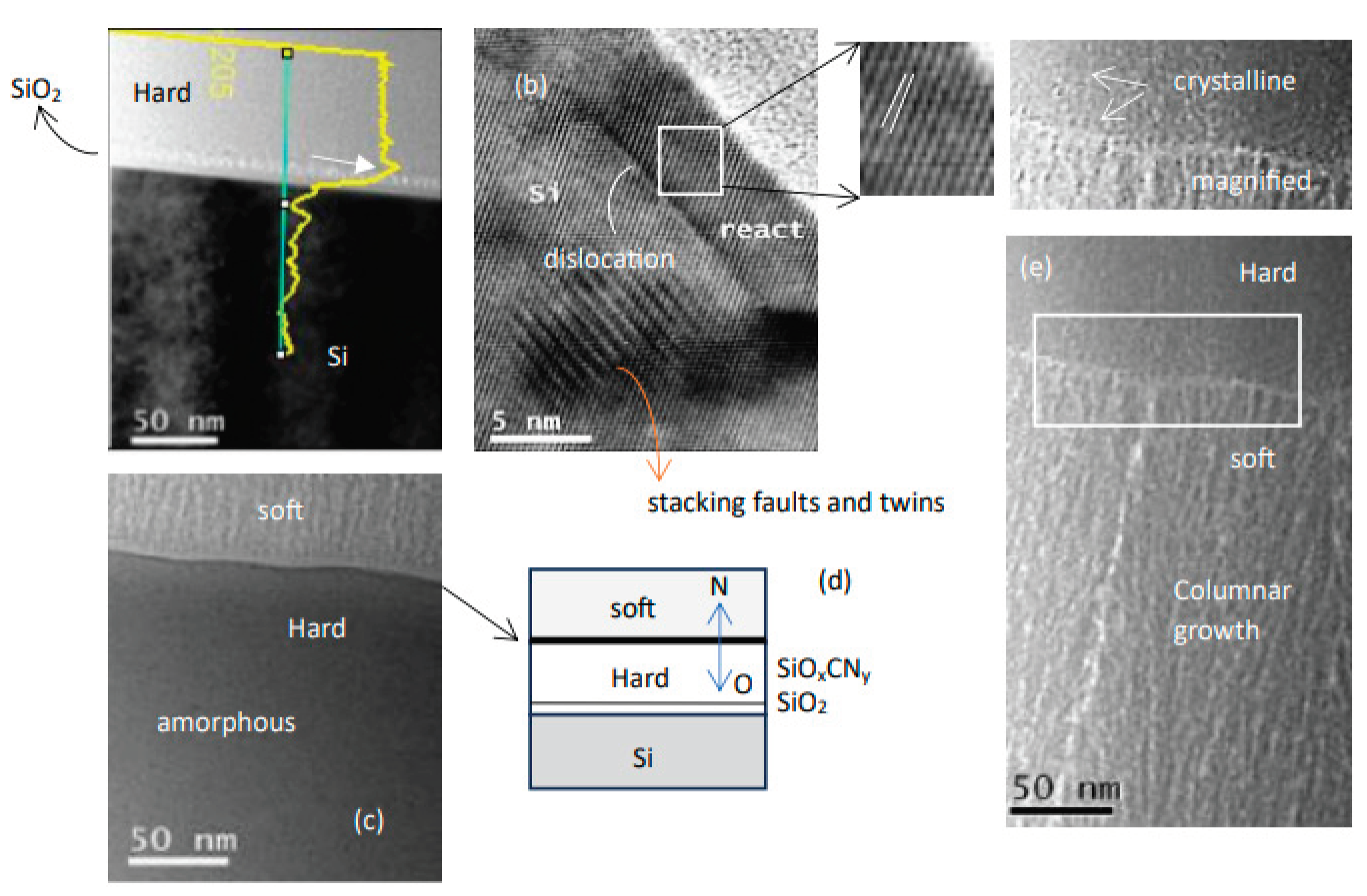
An interface cross sectional study of hard-soft-hard multilayered Si-C-N films on silicon substrate. shows the interface of Si substrate and the first hard layer to be consisting a thin SiO2 native oxide line and mainly amorphous Si-C-N. The native oxide usually found on the silicon surface exposed to atmosphere is about 250 nm. The image however shows it to be about 5nm.This is indicative of the fact that it haa almost dissolved in to hard phase leaving a feeble trail of its existence as show by the image analysis line profile (Figure 5a)
Evidence of stacking faults and twins were also observed in the Si substrate (Figure 5b) A higher nitrogen incorporation leads to slower growth rate and columnar crystalline growth which also causes a reduction in hardness as also found in Ti-B-N films. The interface between the Si substrate and the hard Si-C-N phase was found to have a thin native oxide layer while the hard phase was mainly amorphous in nature consisting of Si, C and N elements (Figure 5c). The amorphous nature was due to the rapid growth process and higher oxygen concentration. The formation of SiOxCNy is therefore predominant in the regions close to the substrate, however the relative oxygen concentration with respect to nitrogen (x/y) decrease as one moves further up (Figure 5d) and hence once can observe hints of crystallization (however not columnar) growth in the hard phase followed by the softer SiCN film, as observed in the magnified view with changed contrast (Figure 5e). The non-columnar growth accounts for the enhanced toughness.
The Ti-B-Si-C-N coating may have formed amorphous regions locally just below the top hard surface and may account for the 30 GPa plot (region A) in Figure 4b. The harder phase might have formed there after (region B). The dislocation restriction occurs in this region C which accounts for reappearance of the softer phase and a change in crystalline nature. The interface region having more percentage of N than O could have led to the formation of Ti-O-B-Si-C-N based softer amorphous phases. A further investigation is required in this matter to confirm the claims made.

4. Conclusions

  • The crystalline structure of the SiCN films regulated the formation of electrical conduction channels with ductile fracture and linear unloading.
  • Tip bluntness causing the substrate effect to be obtained at higher depths of penetration
  • When nitrogen was added to Ti-B-Si-C, Si-C-N instead of TiC or TiB2 formed, which resulted in a decrease in hardness. due to formation of alternate harder and softer films
  • The oxide at the interfacial region is responsible for the amorphization of the hard films developed on the silicon whose relative concentration with nitrogen decreases as one moves further away from the substrate

References

  1. A. Karimzadeh et al Sci Rep 9, 15763 (2019).
  2. M. Wang, Acta Mechanica Solida Sinica 36(2), 327 (2023).
  3. Z. Hu Micro Nano Tech 6 165 (2017).
  4. Y. Sato, Nat Commun 11, 4177 (2020).
  5. W. C. Olver, G.M. Pharr J. Mater Res 7(6), 1564 (1992).
  6. A. C. Fischer Cripps, Nanoindentation, Springer (2004).
  7. X. Li, B. Bhushan Materials Characterization, 48(1) 11(2002).
  8. V. Maier-Kiener et al JOM 74, 2177 (2022).
  9. L.M. Oyen ed. Handbook of nanoindentation: with biological applications. CRC Press (2019).
  10. G. Wu et al Sci Rep 10.1 18784 (2020).
  11. B.Cantor et al Mater Sci Eng: A, 375–377, 2004, 213(2004).
  12. B.Cantor, Ann. Chim. -Sci. Mater. 2007, 32, 245(2007).
  13. E.P. George et al Nat Rev Mater 4 (2019) 515–534.
  14. W. Li, et al Prog Mater. Sc. 118 (2021) 100777.
  15. S. Sinha et al Sci Rep 9, 6639 (2019).
  16. X. Jin et al Ceram Int. 48 (23A) 135445(2022).
  17. G. Laplanche et al, J. Alloys Compd. 647, 548 (2015).
  18. B. Gludovat et al. JOM 67, 2262 (2015).
  19. A. Gali et al George, Intermetallic 39, 74 (2013).
  20. M. Mirkhalaf et al Sci Rep 11, 6951(2021).
  21. Shah, S. Ret al. Acta Mater. 2002, 50(16), 4093–4103. [Google Scholar] [CrossRef]
  22. Riedel, Ret al. Nature 1995, 374(6522), 526–528.
  23. Ren, Z. Materials 2021, 14, 614.
  24. Barrios, EMol. Syst. Des. Eng. 2020, 5(10), 1606–1641.
  25. Lin, X. , Ceram Int. 2023, 49 (14A), 23851–23863. [Google Scholar] [CrossRef]
  26. Geng, T. B. Rare Metals, 2023, 42(5), 1635-1644.
  27. Xue, J. , J Al Com, 2023, 931, 167499.
  28. Han, D. et al J Mater Chem C, 2023, 11(18), 6130-6137.
  29. Wu, C. , et al Chemical Engineering Journal, 2023, 463, 142518.
  30. Chen, G. Surf Coat Technol, 2023,464, 129536.
  31. Li, L. Polymers, 2023 15(15), 3319.
  32. Cui, Z. , Sensors and Actuators A: Physical, 2023, 350, 114144.
  33. Ma, Ket al. IEEE 73rd (ECTC) conference 2023 1110-1114.
  34. Stiharu, I. , Micromachines, 14(5), 925.
  35. Xia, X et al Materials, 16(15), 5318.(2023).
  36. Choi, H. J et al. J. Mater Sci, 58(8), 3790-3801. 2023. [Google Scholar]
  37. Liu, K.et al Ceramics International, 49(2), 2296(2023.
  38. Sulyaeva, V. S. Materials, 16(4), 1467.(2023).
  39. Tomastik, J.; et al Sci. Rep. 2018, 8 (1).
  40. Bernauer, J Adv Eng Mater. 2024, 10.1002/adem.202301864.
  41. Bernauer, J Adv Eng Mater. 10.1002/adem.202301820 (2024).
  42. Thor, Nathalie et al. J Eur Ceram Soc. 2023 43 (4) 1417–1431.
  43. Zhu, Runqiu et al J Am Ceram Soc10.1111/jace.19715.
  44. Wang, Beibei et al J. Mat Sci: Mater in Elect. 35. 10.1007/s10854-024-11941-w.
  45. Ye, Xiao-et al. Physical Chemistry Chemical Physics. 25. 10.1039/D3CP03236A. 2023.
  46. Chiang, Chao-Ching Materials. 16. 5751. 2023.
  47. Qiang Yan, et al J Eur Ceram Soc 2023, 43 (16) 2023, 7373-7380.
  48. Yan, Yuangao et al J Am Ceram Soc. 2023, 106(11), 6951-6961.
  49. Anand, J Am Ceram Soc.2023 107(3), 1657-1668.
  50. Chery, Emmanuel et al. IEEE Tran on Device and Mater Rel 2023 23, 615–622.
  51. Ramlow, Heloisa et al. Open Ceramics. 2023 14. 10 0351.
  52. H. Ramlow J Mater Sci: Mater in Electronics. 34.2023, (22) 1631.
  53. Ramlow, Heloisa et al J. Europ Ceram Soc. 2024 10.1016/j.jeurceramsoc.2024.01.035.
  54. d'Eril, Marco et al Batteries & Supercaps. 2023 6 (3) e202200491.
  55. Li, Qiang et al. J Mater Res Technol. 2021 15, 460–467.
  56. Jiang, Minming et alCeram Int. 2021,48 (2) 2112-2117.
  57. Das, S et al. Silicon 2022, 14, 9643–9657.
  58. Haofan, Shi et al . J. Mater Sci: Mater Elect. 2023, 34. 1401.
  59. Matar, Samir et al. Silicon. 2022 15. 511–520.
  60. Bhattacharyya, AS, et al, Chem Phys Imp 2024, 8,100454(2024).
  61. Bhattacharyya, A. S et al Eur. Coat. J. 2009, 3, 108–114. [Google Scholar]
  62. Bhattacharyya, A. S et al . J. Raman Spectrosc. 2010, 41(10), 1234–1239. [Google Scholar] [CrossRef]
  63. Bhattacharyya, AS et al J. Vac. Sci. Technol A 2010, 28, 505(2010).
  64. Wu, C. et al. Small, 2023, 19(5), 2206628.
  65. Lida Xu, Xiong Zhou, Fuxin Zhao, Yanzhang Fu, Lantian Tang, Yingjun Zeng, Guochun Chen, Chao Wu, Lingyun Wang, Qinnan Chen, Kai Yang, Daoheng Sun, Zhenyin Hai, Journal of Colloid and Interface Science,658,2024,913-922.
  66. S. Veprek Thin Solid Films, 317, 449(1998).
  67. M. Char et al Adv. Eng. Mater. 24, 2100679 (2022).
  68. A.S. Bhattacharyya, et al Next Materials 3, 2024, 100038.
  69. A.S. Bhattacharyya, Chem Phy Imp 8 100551(2024).
  70. A. S. Bhattacharyya, Fatigue & Frac Eng Mater & Str (2024) https://doi.org/10.1111/ffe.14198. [CrossRef]
  71. Ritambhara Dash, A. S. Bhattacharyya Fatigue & Fracture of Eng Mater & Struc. (2023) 46 (7) 2714-2719.
  72. R. Dash, K. Bhattacharyya, A. S. Bhattacharyya., Fatigue & Fracture of Eng Mater & Struct (2023) 46: 1641-1645.
  73. R. Dash, R. P. Kumar, K. Bhattacharyya, A. S. Bhattacharyya, IOP- Eng Res Exp, 2022 4 045012.
  74. R. Dash, K. Bhattacharyya, A S. Bhattacharyya., Nano. Prec. Eng. 6, Eng. 6, 042001 (2023).
  75. R. Dash, K. Bhattacharyya, A.S. Bhattacharyya. Eng Fail Anal (2023) 150, 107353.
  76. A S Bhattacharyya et al Res Surf Int, 2024, 100196.
  77. A. S. Bhattacharyya, R. Praveen Kumar, V. Ranjan, Gaurav Kumar, Current Smart Materials 2(1): 39 – 43, 2017.
  78. T. Sinani and G. Miskovic, 2022 IEEE 24th Electronics Packaging Technology Conference (EPTC), Singapore, Singapore, 2022, pp.452‐458.
  79. R. Dash, K. Bhattacharyya, A S. Bhattacharyya, Int J. Ref Met & Hard Mater, 116, 2023 106373.
  80. S. K. Mishra, D. Verma, S. Bysakh, L. C. Pathak J. Nanomat, 2013, 949416.
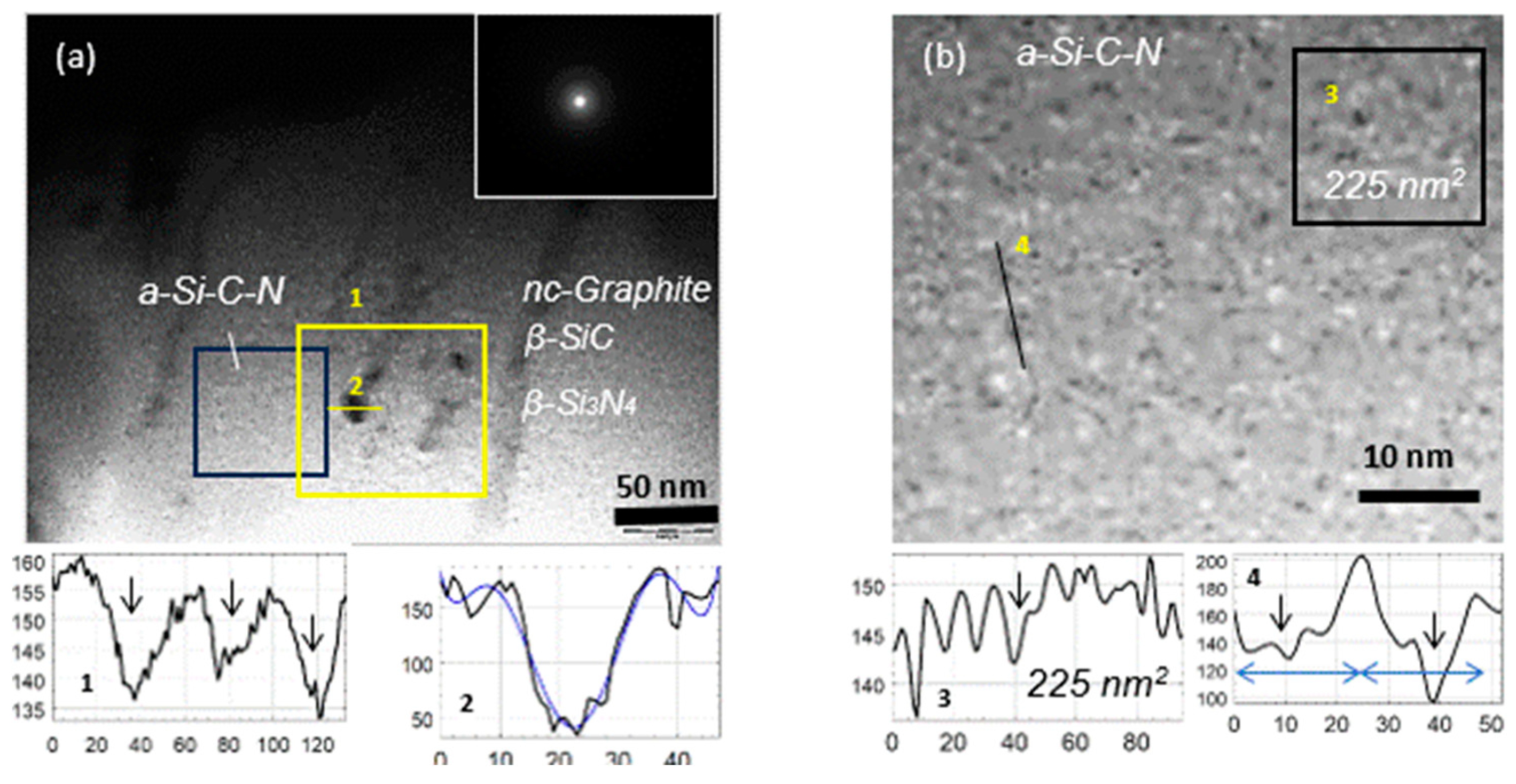
Figure 1. TEM micrograph of Si-C-N coatings deposited at 100 oC showing deposition of crystallites of size ~ 5 nm in the amorphous Si-C-N matrix and corresponding SAED pattern representing amorphous phase (inset) (b) Magnified view of the amorphous region showing the formation of ultrafine crystallites with surface and line profiles of the marked regions (open access) [74].
Preprints 103295 g001
Figure 2. (a) Hardness profile during nanoindentation on SiCN coatings indicating obtained hardness of 24 GPa and a decrease from 40 nm onwards due to substrate effect and (b) the effect of tip bluntness causing the substrate effect to be obtained at higher depths of penetration(schematic) [62,63].
Preprints 103295 g002
Figure 3. Scratch adhesion test performed on SiCN/glass substrate showing failure at 8N critical load (LC) where (b) a sudden release of strain energy causing brittle failure takes place [76].
Preprints 103295 g003
Figure 4. (a)Ti-B-Si-C-N coating with 15GPa hardness (b) Ti-B-Si-C coating with above 40 GPa hardness.
Preprints 103295 g004
Figure 5. (Cross-sectional study of hard-soft Si-C-N coatings on Si with (a) Si-Hard Si-C-N (b)magnified view of (a) and (b) hard-soft Si-C-N (d) schematic of the multilayer with formation of two different interfaces€ hard-soft film interface-open accees CC BY [80].
Preprints 103295 g005
Table 1. PDC based nanocomposites coatings.
S. No Composites/Coatings Properties Reference
SiC/(Hf,Ta)C(N)/(B)C;
SiHfTa(B)CN coatings;
Exceptional high hardness and thermal cycle stability; crack-free; amorphous, good adhesion [40,41]
Si(HfxTa1-x)(C)N residual carbon triggered decomposition reaction, resulting in the formation of Transition Metal Carbides, gaseous nitrogen and SiC, tetragonal hafnium oxide (t-HfO2) within the SiCN matrix-improved phase stability and oxidation resistance [42,49]
Ni–Fe–C/HfO2 /SiCN;
SiCN/MWCNT
metal-organic framework (Ni–Fe–MOF) and hafnium dioxide (HfO2) nanoparticles; improved brittleness and EM wave absorption; MWCNT-COOH increased the interfacial polarization loss and the conduction loss, improving microwave absorbing performance. [43,44]
Penta-SiCN monolayer; SiCN embedded carbon (SiCN–C); Porous SiCN(O) low diffusion energy barrier and robust wettability useful in anode material for Li-ion batteries; stable cycling with a charge capacity, Reversible Na Plating/stripping Reaction for sodium metal batteries [45,51,54]
SiCN-coated implants Hydrophobicity and Antibacterial Properties, replacing Ti implants to avoid Peri-implantitis [46],
PDC SiCN Free carbon enriched interface, high conductivity, strain gauge [64
polymer-derived SiBCN;
PDCs-SiCN(BN)
High-temperature sensing due to good thermomechanical properties, hexagonal boron nitride (h-BN) with weakened polarization relaxation behavior, reduced porosity, and resistance to crack expansion causes low dielectric loss and high-temperature resistance [47,48]
SiCN–SiCN wafer-to-wafer hybrid-bonding next generation of 3D Systems-on-Chip with interconnect densities above 10 mm-2 [50]
C/SiCN and SiCN(O) nanofiber, nonwoven tunable electrical conductivity, EM reflection shielding in the 5G C-band, and
thermo-oxidation resistance
[52,53]
Sputtered SiCN coatings Photoelectric properties, SiCN-based MEMS pressure sensors. [55,56]
CVD-grown SiCN coatings Increased intensity of Si-N-Si, decreased crystallite size with temperature along with increased hardness and modulus [57]
Disclaimer/Publisher’s Note: The statements, opinions and data contained in all publications are solely those of the individual author(s) and contributor(s) and not of MDPI and/or the editor(s). MDPI and/or the editor(s) disclaim responsibility for any injury to people or property resulting from any ideas, methods, instructions or products referred to in the content.
Copyright: This open access article is published under a Creative Commons CC BY 4.0 license, which permit the free download, distribution, and reuse, provided that the author and preprint are cited in any reuse.
Prerpints.org logo

Preprints.org is a free preprint server supported by MDPI in Basel, Switzerland.

Subscribe

© 2024 MDPI (Basel, Switzerland) unless otherwise stated