1. Introduction
Carbon Nanotubes (CNTs) are one-dimensional nanostructures distinguished by their exceptional electrical, mechanical, and optical properties. Since their discovery by Iijima in 1991 [
1], considerable attention has been garnered by CNTs for their potential across a spectrum of applications, including sensors, transistors, solar cells, and flexible electronics. A significant challenge in harnessing the potential of CNTs lies in assembling them into macrostructures such as films, fibers, and papers, which retain their intrinsic properties and facilitate integration with other materials and devices. Among these structures, CNT papers, also known as Buckypapers (BPs), consist of thinly veiled, randomly entangled CNTs and can be produced via the vacuum filtration of CNT suspensions [
2,
3,
4,
5]. BPs have been demonstrated to exhibit photovoltaic properties under various light sources and intensities, such as photocurrent generation and photoconductivity modulation [
6,
7]. However, the photovoltaic performance of BPs is constrained by their low light absorption and carrier concentration, which can be ameliorated by integrating additional materials like metal oxides that can act as light absorbers, charge carriers, or catalysts [
8,
9].
Zinc Oxide (ZnO) is a widely utilized wide-bandgap semiconductor for optoelectronic applications such as dye-sensitized solar cells and photocatalysts [
10,
11]. ZnO offers several advantages, including high electron mobility, high transparency, low cost, and eco-friendliness [
12,
13,
14,
15]. ZnO can be deposited on various substrates, including CNTs, through different methods such as Physical Vapor Deposition (PVD), Chemical Vapor Deposition (CVD), and sputtering [
16,
17,
18]. Sputtering is a versatile and controllable technique capable of producing uniform, high-quality ZnO films with adjustable properties like thickness, morphology, crystallinity, and doping [
19,
20]. It can also be employed to create gradient structures of ZnO on CNTs, inducing a gradient in carrier concentration and enhancing the composite's photovoltaic response [
21,
22]. Furthermore, sputtering followed by subsequent thermal annealing can reduce defects, enhance crystallinity, and promote interfacial bonding, thereby improving the quality and performance of ZnO films [
23,
24].
In this study, we enhanced the photovoltaic characteristics of BPs by sputtering ZnO films onto them and subsequently annealing at various temperatures and durations. We investigated the impact of sputtering parameters, such as gas ratios, power, and time, on the morphology, composition, and resistivity of the ZnO films. Additionally, we measured the photocurrent and photovoltage of the ZnO/BP composites under different light sources, intensities, and modes, such as uniform and gradient illumination. We compared the photovoltaic performance of the ZnO/BP composites to that of the pristine BPs and discussed the potential mechanisms behind the observed phenomena. Our findings aim to optimize the ZnO-BP composite material for optoelectronic applications, showcasing the potential of BPs as flexible and functional substrates for nanomaterials.
2. Experimental Procedure
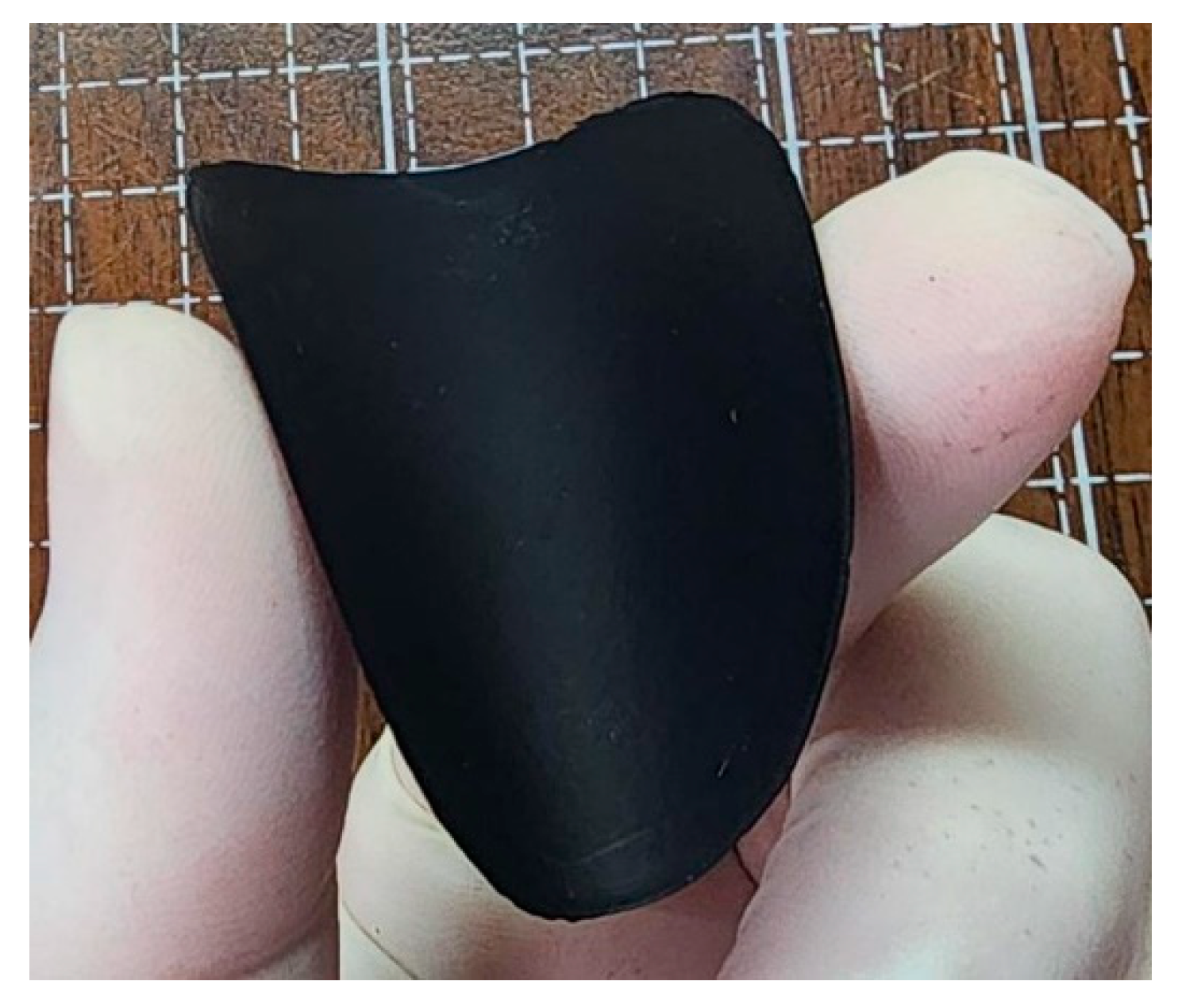
In the present study, the Buckypaper (BP) was fabricated starting with the dispersion of approximately 0.06 grams of Multi-Walled Carbon Nanotubes (MWCNTs) in a dilute solution containing the surfactant Triton X-100. This mixture was then subjected to ultrasonic disruption using an ultrasonicator set at 50W to disperse the nanotubes. The preparation process was completed through a vacuum filtration technique. The MWCNTs featured an average tube diameter of 10-20 nanometers and a length ranging from 60 to 100 micrometers. The finished BP had a diameter of approximately 4.5 centimeters and a thickness of about 75 micrometers, with a porosity of 78%, as illustrated in
Figure 1 below. Subsequently, the BP was cut into several rectangular pieces measuring 2.0 cm x 0.5 cm for further experimentation under varying conditions.
The ZnO films were deposited on Buckypaper (BP) using a pure zinc target (99.99%) with a diameter of 1.5 inches through the Radio Frequency (RF) sputtering process. The vacuum chamber was initially evacuated to a pressure of 5×10^-5 torr using a mechanical pump in conjunction with a turbo molecular pump, after which a mixture of argon and oxygen gases was introduced at different flow ratios. The working gas pressure during sputtering was maintained at 30 mtorr. The distance between the target and the substrate was set to 10 cm, and the substrate was mounted on an electric rotating platform spinning at 10 rotations per minute to ensure uniform deposition. The sputtering power was fixed at 100 watts, and the deposition times were varied at 5, 10, 20, and 40 minutes, respectively. To measure the thickness of the ZnO films, silicon substrates were placed alongside the BP substrates, and the thickness of the ZnO deposited on the silicon was measured using a profilometer, as shown in
Table 1 below.
Further in our study, ZnO-modified BPs, which had been sputtered for 5, 20, and 40 minutes, underwent Rapid Thermal Annealing (RTA) in a fast thermal processing system. The RTA vacuum quartz tube was evacuated to approximately 20 mtorr before the samples were rapidly heated using infrared lamps. The heating rate brought the temperature up to 400°C in five minutes, where it was maintained for 10 minutes, after which the samples were cooled to room temperature via water circulation before being removed from the vacuum chamber.
The morphology and composition of the ZnO-modified BP were observed using a Field Emission Scanning Electron Microscope (FESEM, Joel JSM-7000F) and analyzed by Energy Dispersive X-ray Spectroscopy (EDS). The crystalline structure of the ZnO-modified BP was determined through X-ray Diffraction (XRD) analysis using a Philips X'Pert Pro MPD system with Cu Kα radiation. The resistivity of the ZnO-modified BP was measured using the four-point probe method with a Keithley 2400 source meter. The photovoltaic characteristics of the ZnO-modified BP were assessed using a solar simulator (A.M. 1.5G) as the light source, with an intensity of 1000 W/m². Photocurrent and photovoltage were recorded using a Keithley 2000 multimeter. The samples were measured under two illumination modes: uniform illumination and gradient illumination. In the uniform mode, the entire area of the sample was exposed to the light source. For gradient illumination, the samples were exposed to a light source with a gradient of intensity, ranging from high to low across their area. This gradient illumination mode was achieved by placing a filter with a gradient in transparency above the samples. Furthermore, the samples were measured under different wavelengths of light, ranging from 400 nm to 700 nm, utilizing red, green, and blue color filters to accomplish this.
3. Results and Discussion
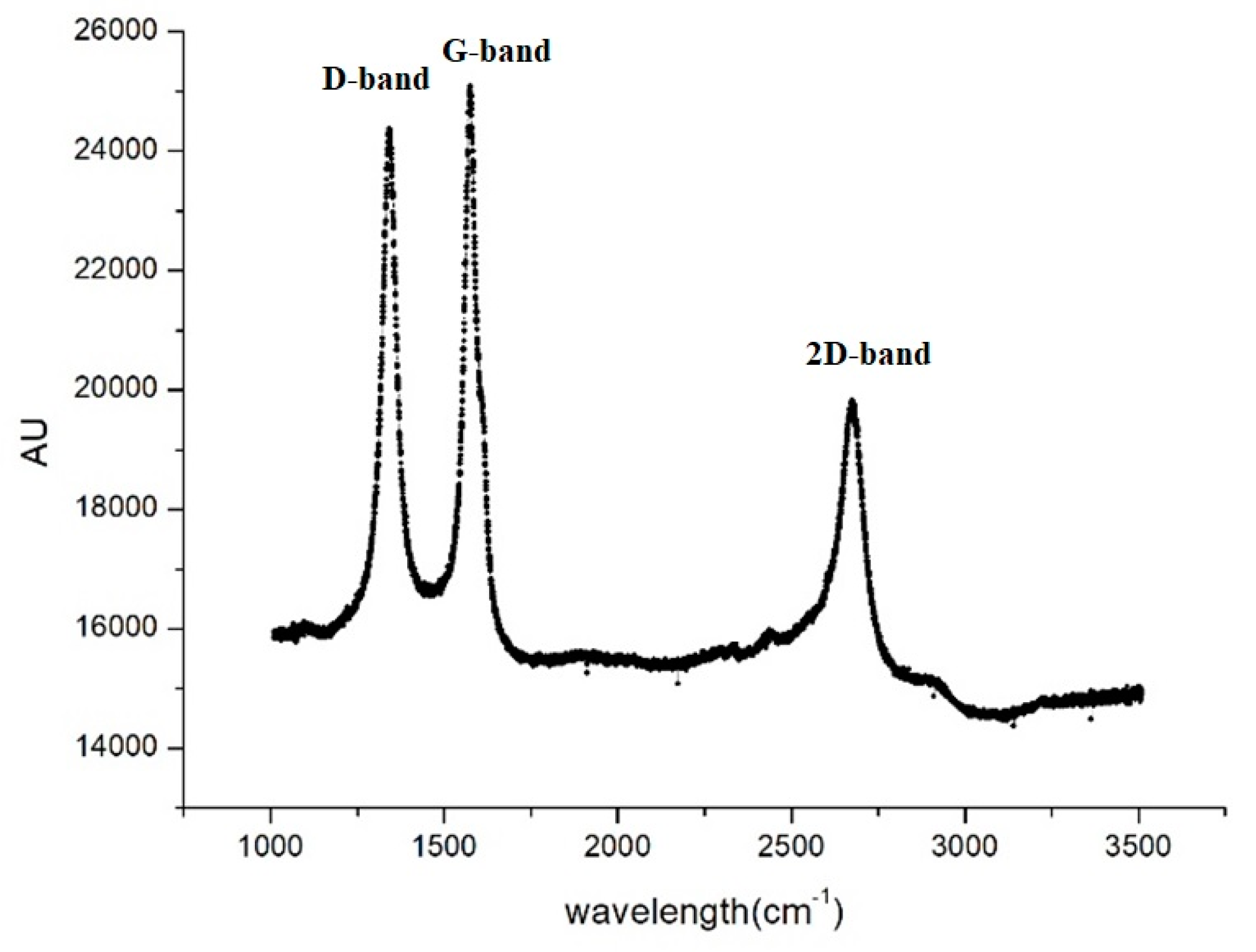
Figure 2 displays the Raman spectrum of pristine Buckypaper (BP), showcasing two characteristic peaks of Carbon Nanotubes (CNTs): the D band at 1350 cm
-1 and the G band at 1580 cm
-1. The D band is associated with disorder and defects within the CNTs, while the G band relates to the in-plane vibrations of sp
2 bonded carbon atoms. The intensity ratio of the D to G bands (ID/IG) reflects the crystallinity and purity of the CNTs. For pristine BP, the ID/IG ratio was found to be 0.99, indicating that the crystalline quality of the CNTs is reasonably acceptable.
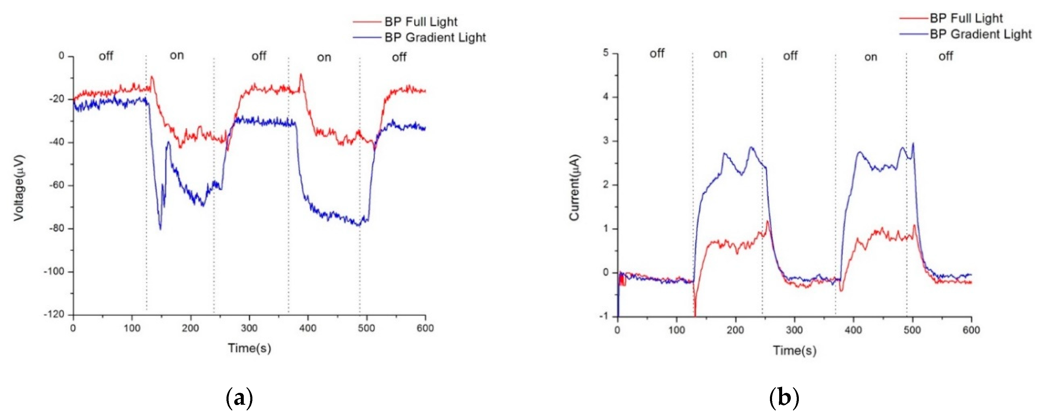
Figure 3a,b respectively depict the photovoltage and photocurrent of pristine Buckypaper (BP) after a sputtering duration of five minutes, under both uniform and gradient illumination conditions. "On" in the figures refers to the state of illumination, while "off" indicates the absence of light. Due to the extensive surface area and dangling bonds in the internal structure of BP, a self-charging phenomenon is often observed during electrical measurements. This effect becomes more pronounced with successive light on/off cycles, leading to an initial voltage deviation even when not illuminated. This initial offset is used for correction to zero in the calculation of photovoltage and photocurrent. Therefore, under uniform illumination, pristine BP generated approximately -18.3 microvolts of photovoltage and 0.8 microamps of photocurrent; under gradient illumination, it produced approximately -35.20 microvolts of photovoltage and 2.60 microamps of photocurrent. Referencing the semiconductor material current density equation (1), the higher photovoltaic response under gradient illumination is attributed to a higher concentration gradient difference within BP, thus increasing the diffusion current of carriers. Additionally, the photovoltaic mechanism in BP can also be explained by the vibration of π bonds and the mobility of π electrons in CNTs when exposed to light.
In this equation, Jp,drift represents the drift current, Jp,diffusion denotes the diffusion current, q is the elementary charge of the carrier, p indicates the concentration of the carriers, μp is the mobility of the carriers, E represents the electric field applied across the semiconductor material, Dp is the diffusion coefficient for the carriers.
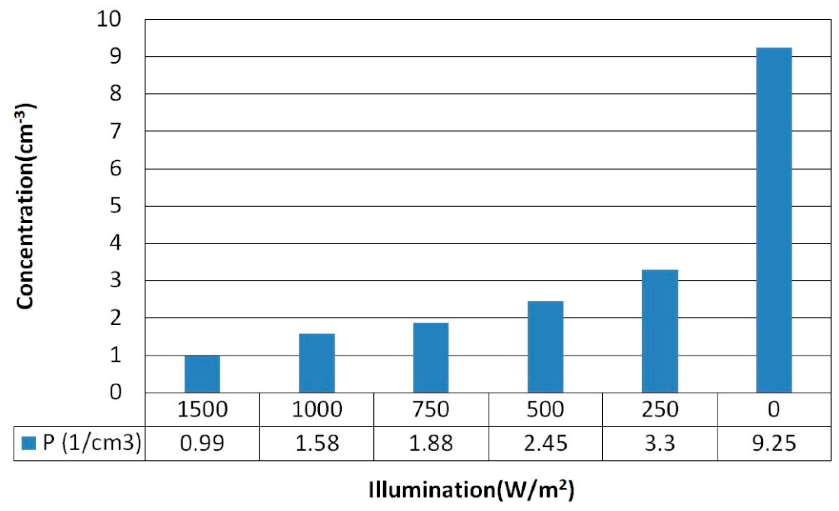
To verify the variation in carrier concentration of Buckypaper (BP) under illumination, we manually adjusted the solar simulator to various light intensities while simultaneously measuring the carrier concentration of pristine BP at different light strengths using the Hall Effect method, with results depicted in
Figure 4. Pristine BP exhibited p-type semiconductor behavior, indicating that the predominant carriers are holes. As the intensity of light increased, the carrier concentration decreased from 9.25×10
18 cm
-3 in the absence of illumination to 0.99×10
18 cm
-3 at an illumination of 1500 watts per square meter. This reduction is conjectured to be due to light-induced electron-hole pair recombination, diminishing the quantity of free carriers in BP.
Following the examination of the fundamental properties of pristine Buckypaper (BP), we embarked on a series of experiments where ZnO material was deposited on BP using different ratios of argon to oxygen gas flow, at a power of 100W, and for a sputtering duration of 5 minutes. We then examined the photovoltaic response of these ZnO/BP composites.
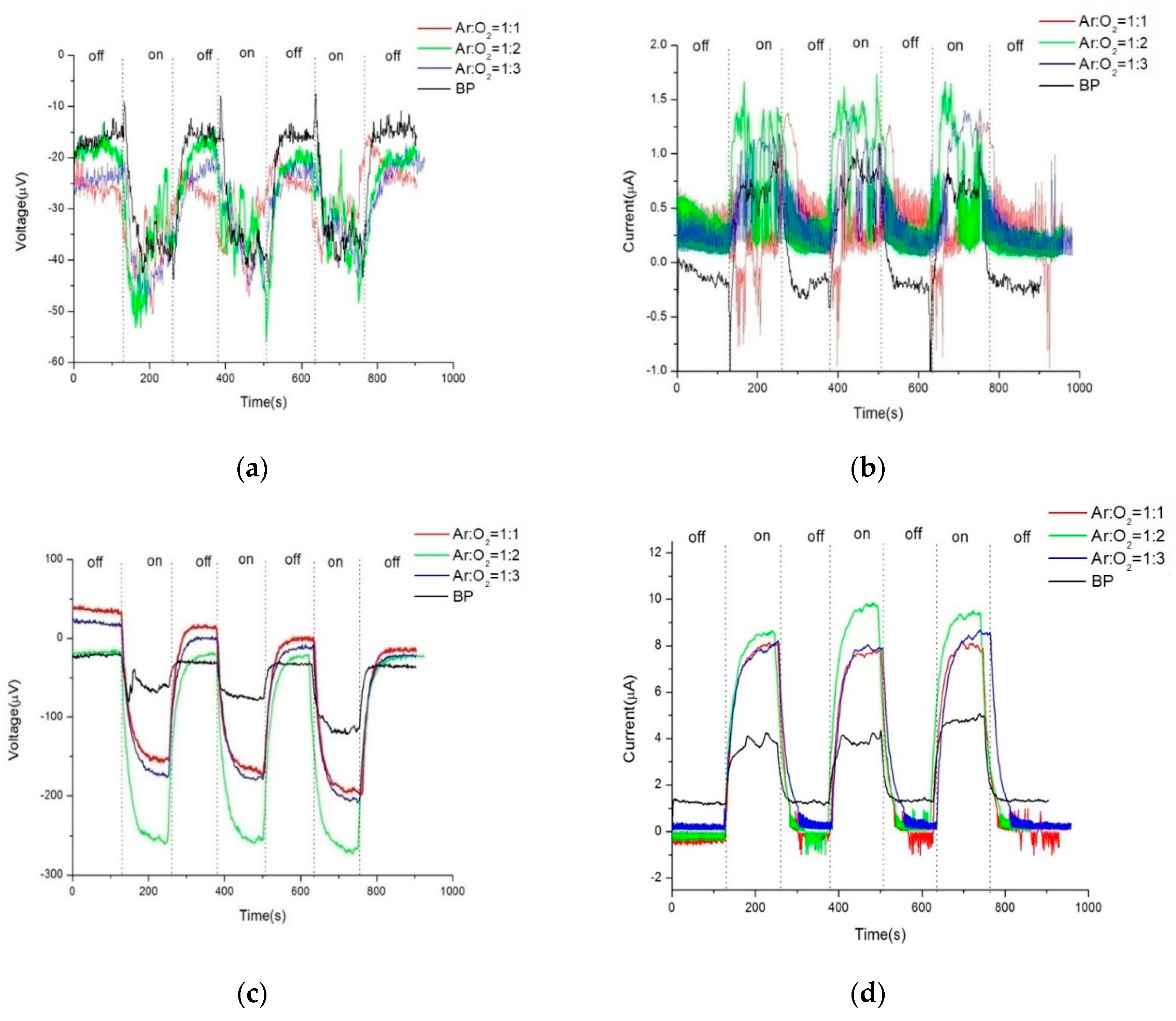
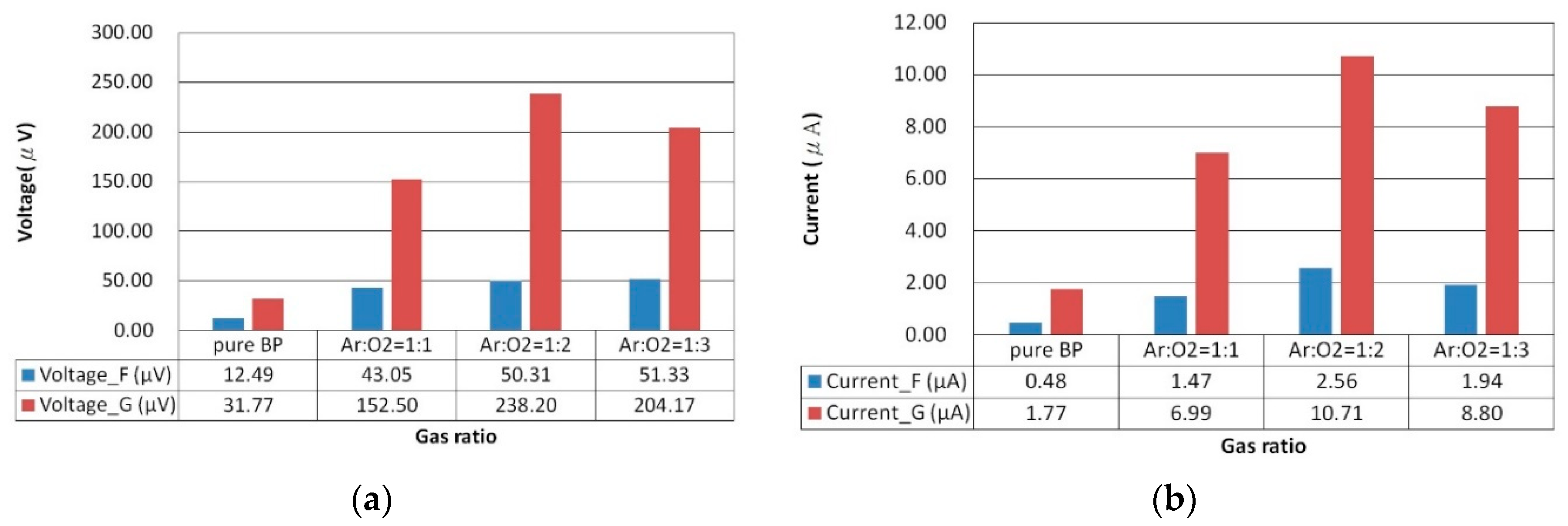
Figure 5a-d illustrate the comparison of photovoltage and photocurrent between pristine BP and ZnO/BP composites under both uniform and gradient illumination conditions. Under uniform illumination, due to grain boundary scattering by the ZnO material, both photocurrent and photovoltage exhibited more pronounced fluctuations during measurement. Conversely, under gradient illumination, the photovoltaic response curves were smoother, attributed to an enhancement in photovoltage energy. Furthermore, compared to pristine BP, the ZnO/BP composites showed a significantly improved photovoltaic response under gradient illumination. The peak values under various experimental conditions are summarized in the following bar graph.
Figure 6 showcases the photovoltage and photocurrent of ZnO films deposited on BP substrates under different argon to oxygen gas flow ratios (ranging from 1:1 to 1:3), observed under both uniform and gradient illumination. For the ZnO/BP composites with an argon to oxygen gas flow ratio of 1:2, the highest photovoltage and photocurrent were recorded under gradient illumination, amounting to -238.20 microvolts and 10.71 microamps, respectively. In contrast, under uniform illumination, the values were only -50.30 microvolts and 1.13 microamps. Therefore, subsequent experiments involving thermal annealing of ZnO were conducted with the argon to oxygen gas flow ratio set at 1:2 for standard ZnO sputtering. The argon to oxygen gas flow ratio impacts the oxidation quality and carrier concentration of the ZnO films, as excess oxygen can decrease the sputtering rate and carrier density, while insufficient oxygen may result in suboptimal ZnO formation. The enhancement in photovoltaic response of the ZnO/BP composites is attributed to the ZnO material's ability to extend the absorption spectrum, increase carrier concentration, and reduce impedance. The superior photovoltaic response under gradient illumination is due to an increase in diffusion current, resulting from higher concentration gradient differences within the ZnO/BP composites.
In addition to measuring the photovoltaic properties, we also sought to understand the crystalline phase changes of ZnO material during growth.
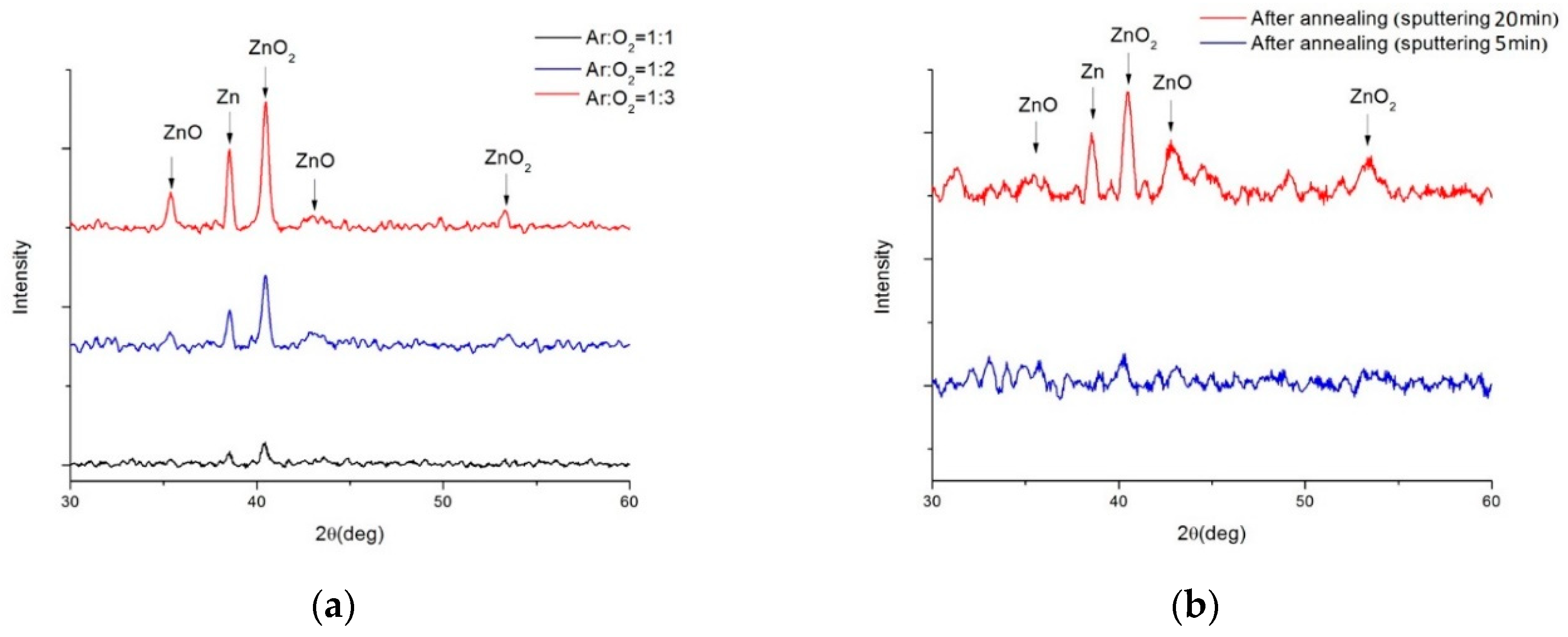
Figure 7a displays the X-ray Diffraction (XRD) patterns of ZnO films deposited on BP for 5 minutes at 100W power under different argon to oxygen gas flow ratios. Due to the overwhelming peak intensities of the carbon material, which were not the focus of our study, their peaks are not shown. The XRD patterns reveal the crystalline structure and phase composition of the ZnO films. The XRD pattern for the argon to oxygen gas flow ratio of 1:3 showed optimal oxidation quality, as it exhibited the highest intensity peaks for ZnO at 35.3° and 42.8°, corresponding to the (002) and (101) planes of the hexagonal wurtzite structure of ZnO, respectively. The XRD pattern for a gas flow ratio of 1:1 displayed peaks for metallic zinc (Zn) at 38.5° and zinc peroxide (ZnO
2) at 40.4° and 53.4°, indicating incomplete oxidation of the zinc target. The pattern for a gas flow ratio of 1:2 showed a mix of ZnO, Zn, and ZnO2 peaks, suggesting medium oxidation quality.
The argon to oxygen gas flow ratio affects the oxidation of the zinc target, as excessive oxygen can decrease the sputtering rate, and insufficient oxygen can lead to suboptimal ZnO formation. However, since the photovoltaic characteristics of ZnO on BP at a gas flow ratio of 1:2 were superior to the other ratios, we continued to sputter ZnO material at this ratio for subsequent experiments.
Figure 7b presents the XRD patterns of ZnO films before and after annealing at 400°C, for a gas flow ratio of 1:2. The annealing process, applied to ZnO films deposited for 5 minutes, is presumed to reduce the intensity of ZnO peaks due to the lower mass of the material, not improving the crystallinity. Conversely, for ZnO deposited for 20 minutes, the post-annealing XRD pattern confirmed the presence of ZnO and CNTs in the ZnO/BP composite, as the ZnO peaks at 35.3° and 42.8° matched well with the CNT peaks at 26.0° and 43.9°, corresponding to the (002) and (100) planes of the graphite structure of CNTs. This indicates that the ZnO film infiltrated into the CNTs, forming a more uniform and compact composite material.
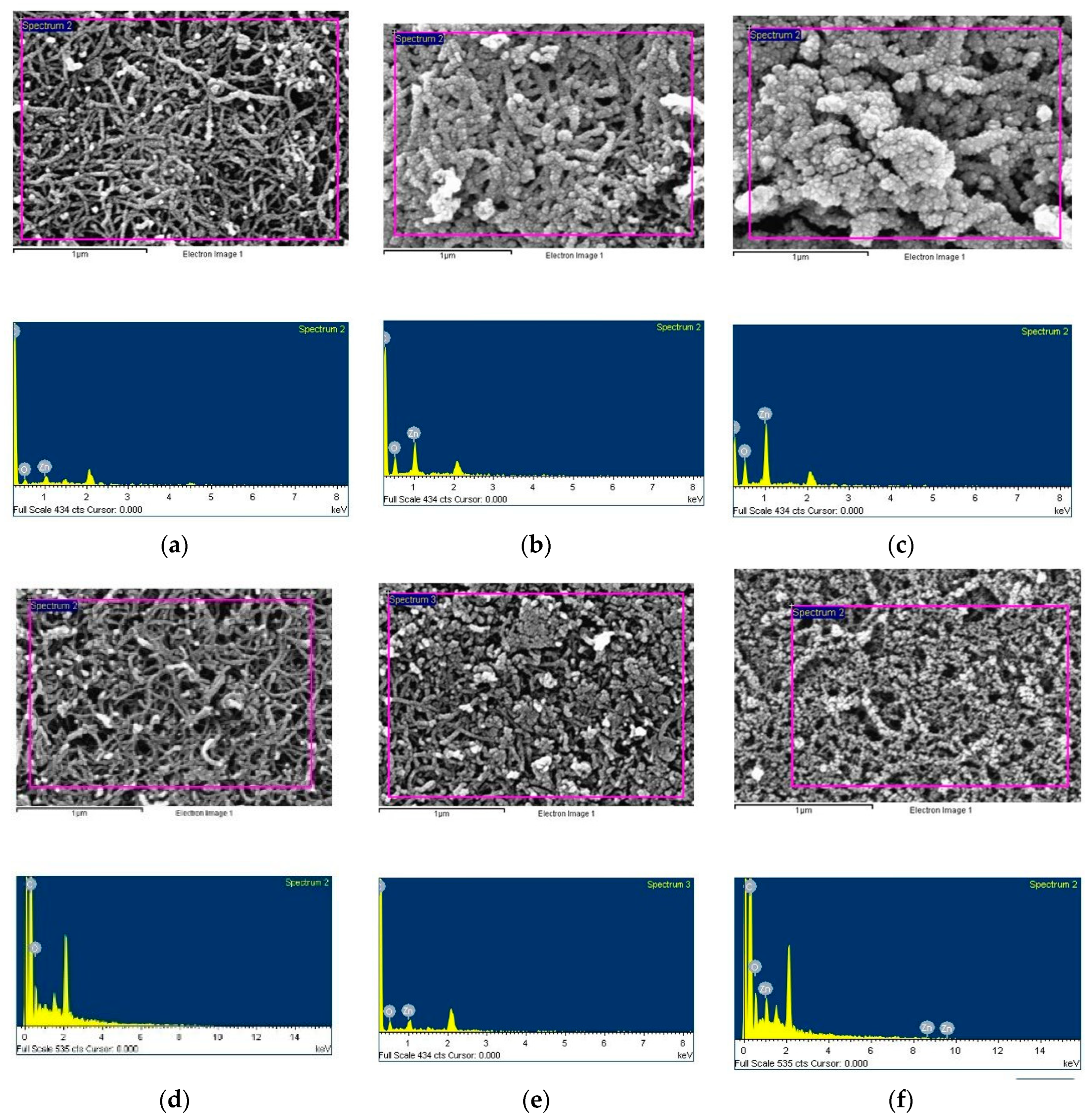
To investigate the effects of annealing on ZnO films, we deposited ZnO on BP substrates for different sputtering durations (5 minutes, 20 minutes, and 40 minutes) with an argon to oxygen gas flow ratio of 1:2. Subsequently, the samples were annealed at 400°C, and their surface morphologies were examined using Scanning Electron Microscopy (SEM), as shown in
Figure 8a-f, while their elemental compositions and ratios were analyzed using Energy Dispersive X-ray Spectroscopy (EDS), as presented in
Table 2. SEM images reveal the morphology and thickness of the ZnO films, and EDS analysis confirms the elemental composition of the ZnO films.
With increasing sputtering time, the ZnO/BP surface sputtered for 5 minutes showed only a slight increase in crystalline grains. For the 20-minute ZnO/BP, the carbon nanotubes were fully enveloped by ZnO grains, whereas for the 40-minute ZnO/BP, the excessive ZnO coverage around the carbon nanotubes led to a significant increase in the average diameter of the nanotubes. The overly thick ZnO hindered light penetration to the carbon nanotubes, thereby reducing photovoltaic efficiency. Furthermore, after annealing, there was a noticeable change in the morphology of the ZnO films; they became thinner and more dispersed on the BP surface. EDS analysis indicated the presence of zinc and oxygen elements in the ZnO films. After annealing, the longer the ZnO sputtering time on BP, the greater the decrease in the ratio of oxygen to zinc on the surface. This reduction is attributed to the infiltration of ZnO into the CNTs and the partial evaporation and loss of material.
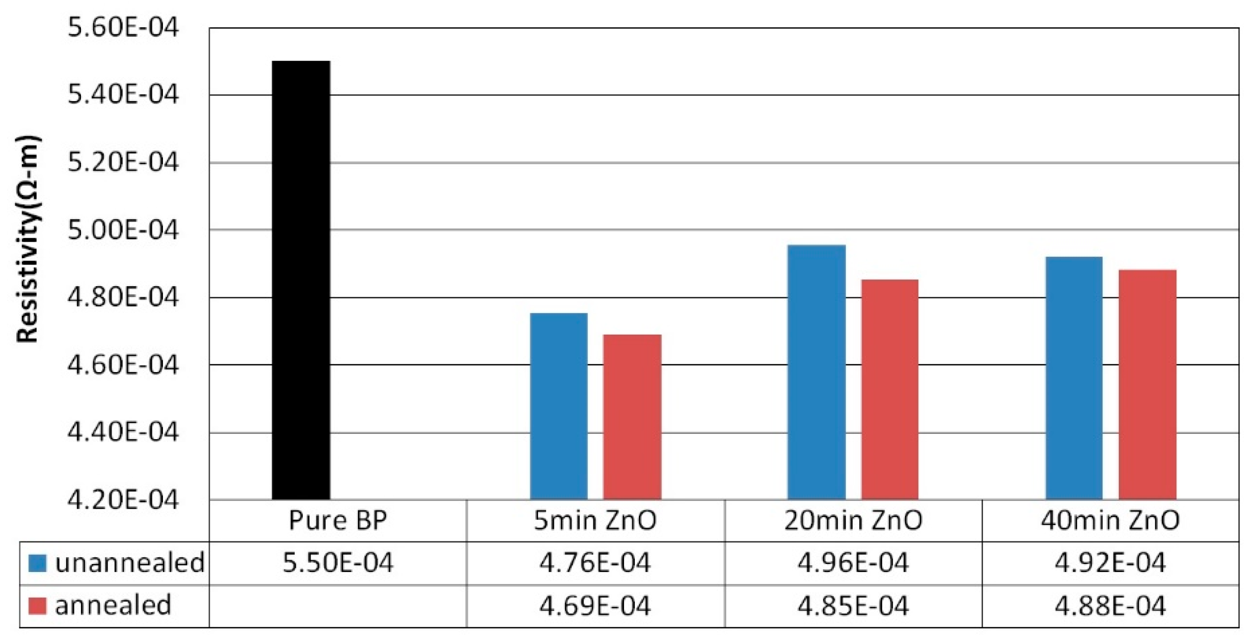
Figure 9 illustrates the resistivity of ZnO films sputtered on BP substrates with an argon to oxygen gas flow ratio of 1:2, for varying sputtering durations (5 minutes, 20 minutes, and 40 minutes), both before and after annealing at 400°C. Post-annealing, the resistivity of the ZnO/BP composite materials decreased, from 4.76×10
-4 ohm-m for the 5-minute sputtering duration to 4.69×10
-4 ohm-m, from 4.96×10
-4 ohm-m for the 20-minute duration to 4.85×10
-4 ohm-m, and from 4.92×10
-4 ohm-m for the 40-minute duration to slightly lower at 4.88×10^-4 ohm-m. The reduction in resistivity after annealing is attributed to a denser structure and larger contact area of the ZnO/CNT composite material, which enhances the transport of carriers.
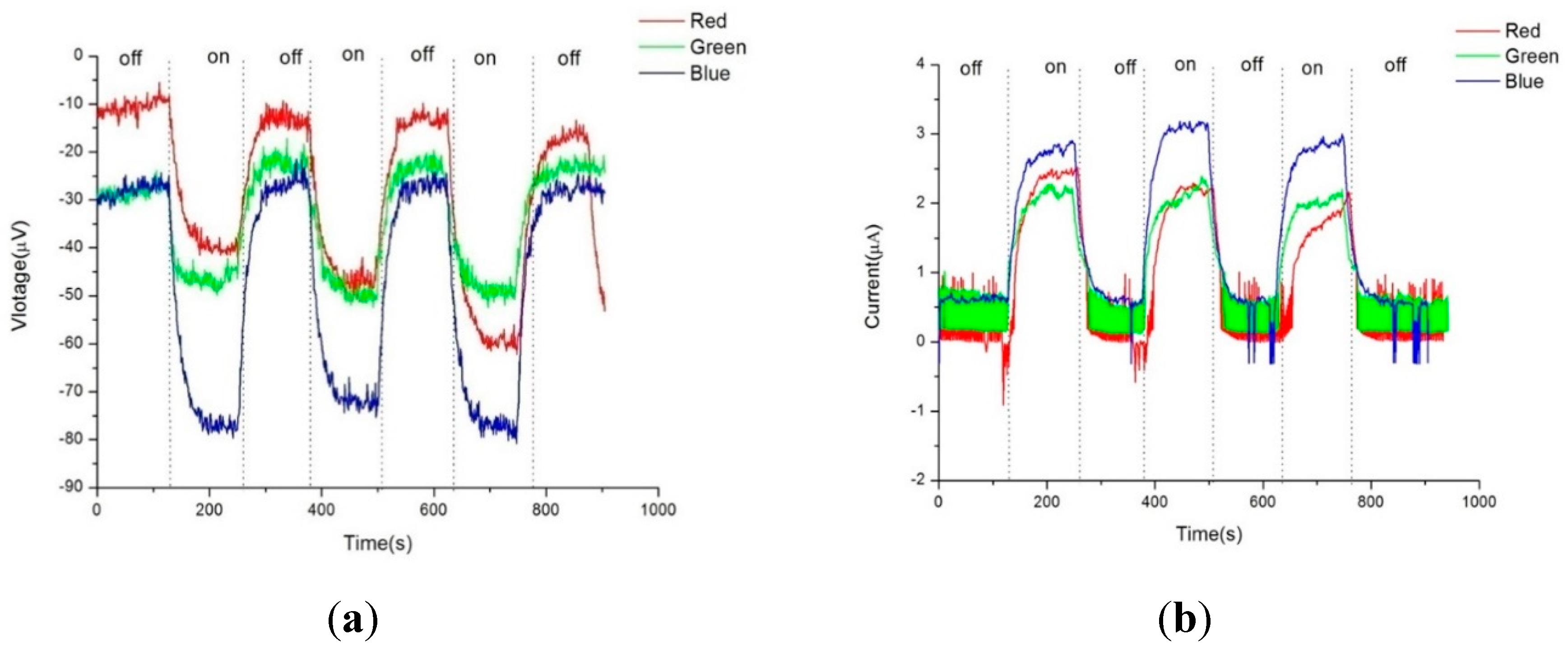
Figure 10 presents the photovoltage and photocurrent of ZnO/BP composite materials with an argon to oxygen gas flow ratio of 1:2, under different wavelengths using RGB color filters. The ZnO/BP composites exhibited the highest photovoltage and photocurrent under blue light. The wavelength dependency of the photovoltaic response of the ZnO/BP composites is attributed to the energy level alignment of the ZnO/CNT heterostructure, which aligns well with blue and ultraviolet light.
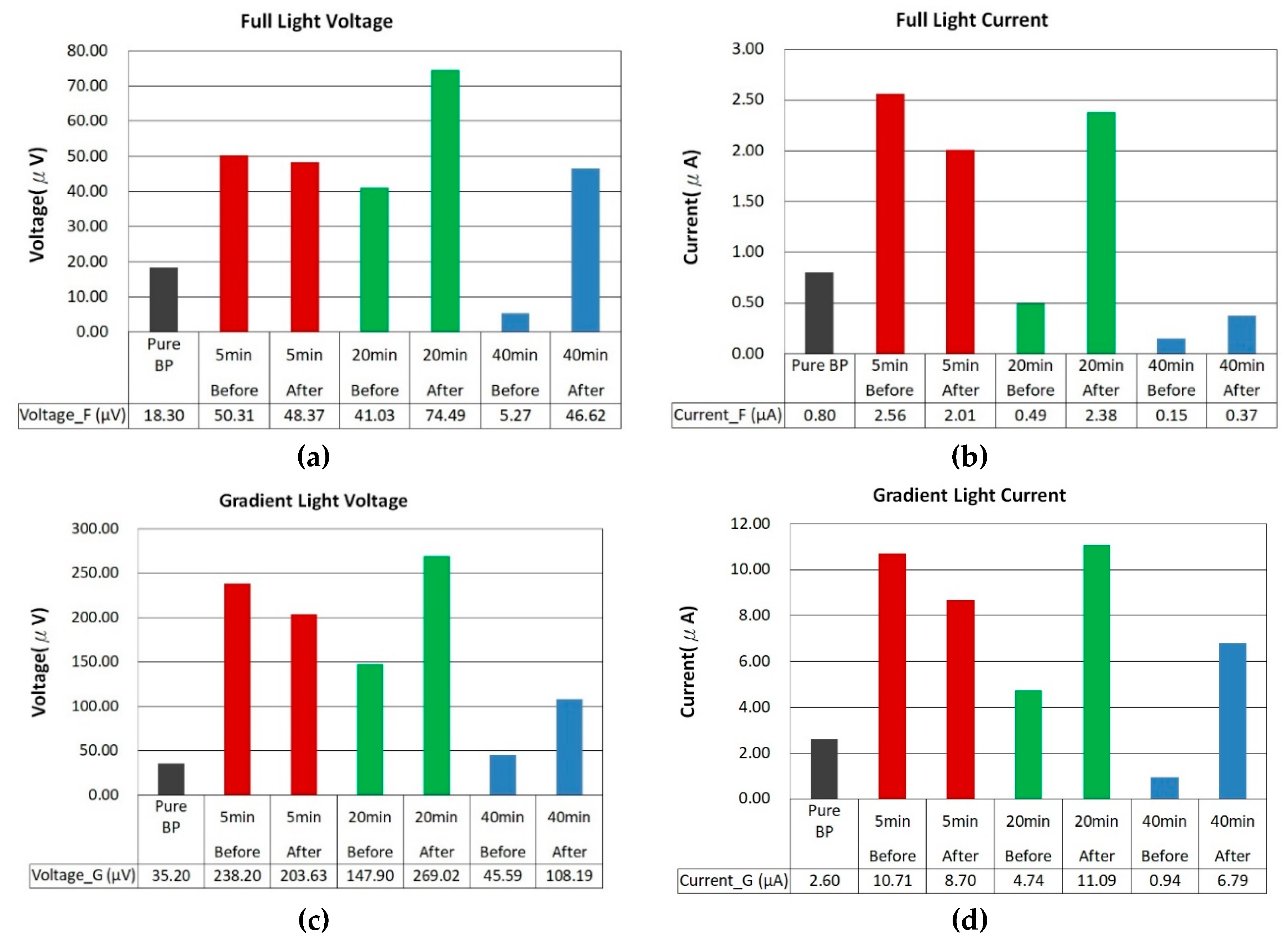
The photovoltaic performance after thermal annealing, as shown in
Figure 11a-d, depicts the photovoltage and photocurrent for ZnO films sputtered on BP substrates with an argon to oxygen gas flow ratio of 1:2, across different sputtering durations (5 minutes, 20 minutes, and 40 minutes), before and after annealing at 400°C, under both uniform and gradient illumination. Before annealing, the ZnO/BP composites with a 5-minute deposition time showed commendable photovoltage and photocurrent, attributed to the infiltration of the ZnO film into the CNTs and the elimination of some impurities. This improved the carrier contact and transport within the ZnO/CNT composite material. However, after annealing, a slight decrease was observed. Based on SEM images from
Figure 8a and (d), it is speculated that the reduced coverage and quantity of ZnO, combined with material loss during annealing, resulted in the remaining scant ZnO failing to further enhance the photovoltaic effect.
Upon closer inspection of the samples with a 20-minute ZnO deposition time, the photovoltage increased from 18.30 microvolts to 41.03 microvolts and then rose to 74.49 microvolts after annealing. Subsequent exposure to gradient illumination further enhanced the photovoltaic effect, ultimately increasing the photovoltage by a total of 14.70 times to 269.02 microvolts. Similarly, the photocurrent saw an overall increase of 13.86 times, reaching 11.09 microamps. In contrast, the samples with a 40-minute ZnO deposition time did not exhibit an enhanced photovoltaic effect due to the excessive modifier material blocking light from reaching the internal BP/ZnO junctions.
For ZnO/BP composite materials, the optimal sputtering duration was found to be 20 minutes, as it showed the highest photovoltage and photocurrent after annealing under both lighting modes. The increase in photovoltage and photocurrent can be attributed to the thicker ZnO film and the formation of the ZnO/CNT heterostructure, enhancing light absorption and carrier separation. The slight decrease in photovoltaic response is due to the reduced light transmittance and increased recombination rate associated with overly thick ZnO films. The higher photovoltaic response of ZnO/BP composites under gradient illumination compared to uniform illumination is due to the increased diffusion current, resulting from higher concentration gradient differences within the ZnO/BP composite material.
Figure 1.
Photo of BP after the vacuum filtration process. BP is ductile, and MWCNTs are evenly distributed.
Figure 1.
Photo of BP after the vacuum filtration process. BP is ductile, and MWCNTs are evenly distributed.
Figure 2.
Raman spectroscopy graph of pure nanotube paper.
Figure 2.
Raman spectroscopy graph of pure nanotube paper.
Figure 3.
a), Photovoltage response of pure buckypaper under full and gradient illumination, (b) Photocurrent response of pure buckypaper under full and gradient illumination.
Figure 3.
a), Photovoltage response of pure buckypaper under full and gradient illumination, (b) Photocurrent response of pure buckypaper under full and gradient illumination.
Figure 4.
Carrier concentration measured in pure buckypaper under different illumination intensities.
Figure 4.
Carrier concentration measured in pure buckypaper under different illumination intensities.
Figure 5.
Photovoltage and photocurrent response under uniform illumination (a,b) and gradient illumination (c,d) of ZnO film deposited on buckypaper for 5 minutes at different argon and oxygen flow rate ratios.
Figure 5.
Photovoltage and photocurrent response under uniform illumination (a,b) and gradient illumination (c,d) of ZnO film deposited on buckypaper for 5 minutes at different argon and oxygen flow rate ratios.
Figure 6.
Photovoltage and photocurrent bar graph of ZnO film deposited for 5 minutes with a plasma power of 100 watts under different argon and oxygen flow rate ratios, under uniform and gradient illumination.
Figure 6.
Photovoltage and photocurrent bar graph of ZnO film deposited for 5 minutes with a plasma power of 100 watts under different argon and oxygen flow rate ratios, under uniform and gradient illumination.
Figure 7.
(a) XRD spectra of ZnO film deposited for 5 minutes under different argon and oxygen flow rate ratios and (b) XRD spectra of ZnO deposited under a flow rate ratio of argon to oxygen of 1:2 for 20 minutes, after annealing.
Figure 7.
(a) XRD spectra of ZnO film deposited for 5 minutes under different argon and oxygen flow rate ratios and (b) XRD spectra of ZnO deposited under a flow rate ratio of argon to oxygen of 1:2 for 20 minutes, after annealing.
Figure 8.
SEM images of ZnO sputtered on buckypaper at an argon and oxygen flow rate ratio of 1:2, (a)-(c) respectively show films deposited for 5 minutes, 20 minutes, and 40 minutes without annealing, and (d)-(f) show films deposited for 5 minutes, 20 minutes, and 40 minutes with annealing.
Figure 8.
SEM images of ZnO sputtered on buckypaper at an argon and oxygen flow rate ratio of 1:2, (a)-(c) respectively show films deposited for 5 minutes, 20 minutes, and 40 minutes without annealing, and (d)-(f) show films deposited for 5 minutes, 20 minutes, and 40 minutes with annealing.
Figure 9.
Resistivity of ZnO films deposited at different sputtering times with a plasma power of 100 watts, before and after thermal annealing.
Figure 9.
Resistivity of ZnO films deposited at different sputtering times with a plasma power of 100 watts, before and after thermal annealing.
Figure 10.
Photovoltage and photocurrent response under uniform illumination of different color lights on ZnO sputtered on buckypaper for 5 minutes with argon and oxygen at a 1:2 ratio.
Figure 10.
Photovoltage and photocurrent response under uniform illumination of different color lights on ZnO sputtered on buckypaper for 5 minutes with argon and oxygen at a 1:2 ratio.
Figure 11.
Comparison of photovoltage and photocurrent before and after annealing of ZnO films deposited on buckypaper at an argon and oxygen flow rate ratio of 1:2 for 5 minutes, 10 minutes, and 40 minutes.
Figure 11.
Comparison of photovoltage and photocurrent before and after annealing of ZnO films deposited on buckypaper at an argon and oxygen flow rate ratio of 1:2 for 5 minutes, 10 minutes, and 40 minutes.
Table 1.
Film thickness of ZnO deposited at different sputtering times.
Table 1.
Film thickness of ZnO deposited at different sputtering times.
| ZnO film thickness |
| Deposition time(min) |
5 |
10 |
20 |
40 |
| Film thickness(nm) |
10 |
20 |
45 |
80 |
Table 2.
EDS analysis of films sputtered with ZnO on buckypaper at an argon and oxygen flow rate ratio of 1:2, deposited for 5 minutes, 20 minutes, and 40 minutes, before and after annealing.
Table 2.
EDS analysis of films sputtered with ZnO on buckypaper at an argon and oxygen flow rate ratio of 1:2, deposited for 5 minutes, 20 minutes, and 40 minutes, before and after annealing.
| EDS |
Sputtering 5min |
Sputtering 20min |
Sputtering 40min |
| |
Before annealing |
After annealing |
Before annealing |
After annealing |
Before annealing |
After annealing |
| Oxygen |
5.73 |
5.48 |
13.59 |
7.57 |
22.05 |
9.64 |
| Zinc |
1.51 |
1.08 |
4.13 |
1.83 |
11.83 |
3.88 |
