Submitted:
15 April 2024
Posted:
16 April 2024
You are already at the latest version
Abstract
Keywords:
1. Introduction
- Prevent attackers from obtaining the execution status of branches;
- Prevent attackers from stealing the jump information of branches;
- Detect the tampering attacks on branch information.
- The branch information protection mechanism based on hardware locking is proposed. When the program is running, this mechanism will calculate the number of updates to BTB. If it exceeds the set threshold, BTB will be locked, preventing attackers from filling up BTB through spy processes, and obtaining the execution status of branches by analyzing the time difference of whether BTB is updated;
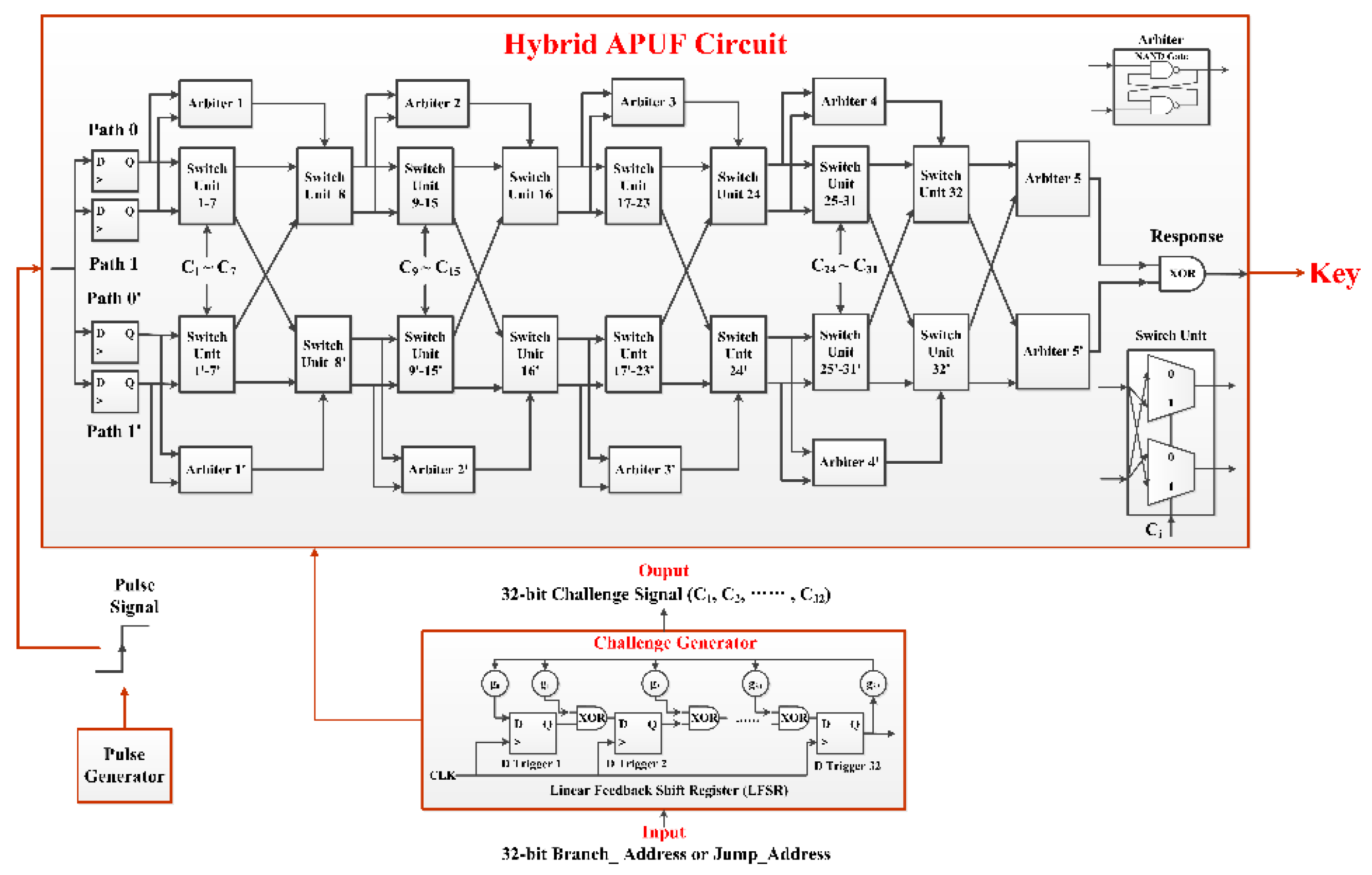
- The branch information protection mechanism based on dynamic isolation is proposed. This mechanism encrypts the branch information (such as branch addresses, jump addresses, and their indexes) and achieve dynamic isolation. This article designs the hybrid Arbiter PUF (APUF) circuit that provides the keys. This circuit can confuses the relationship between the input challenge and the output response, and improves the ability to resist machine learning attacks;
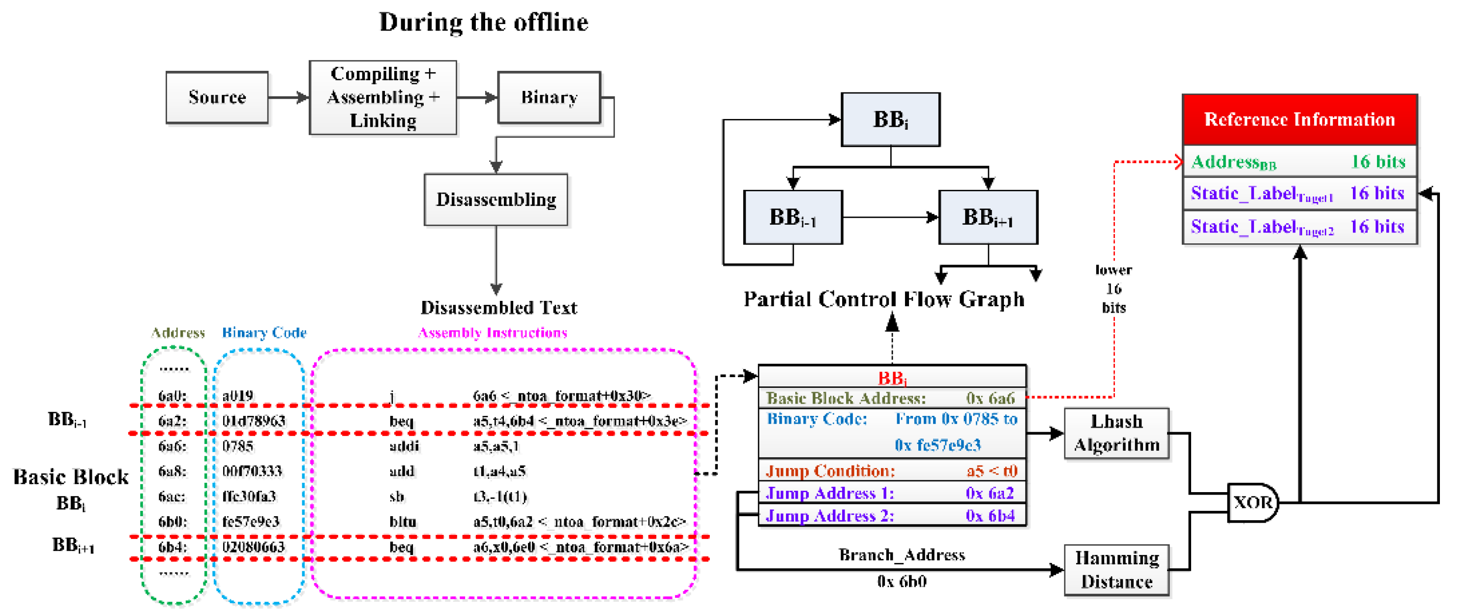
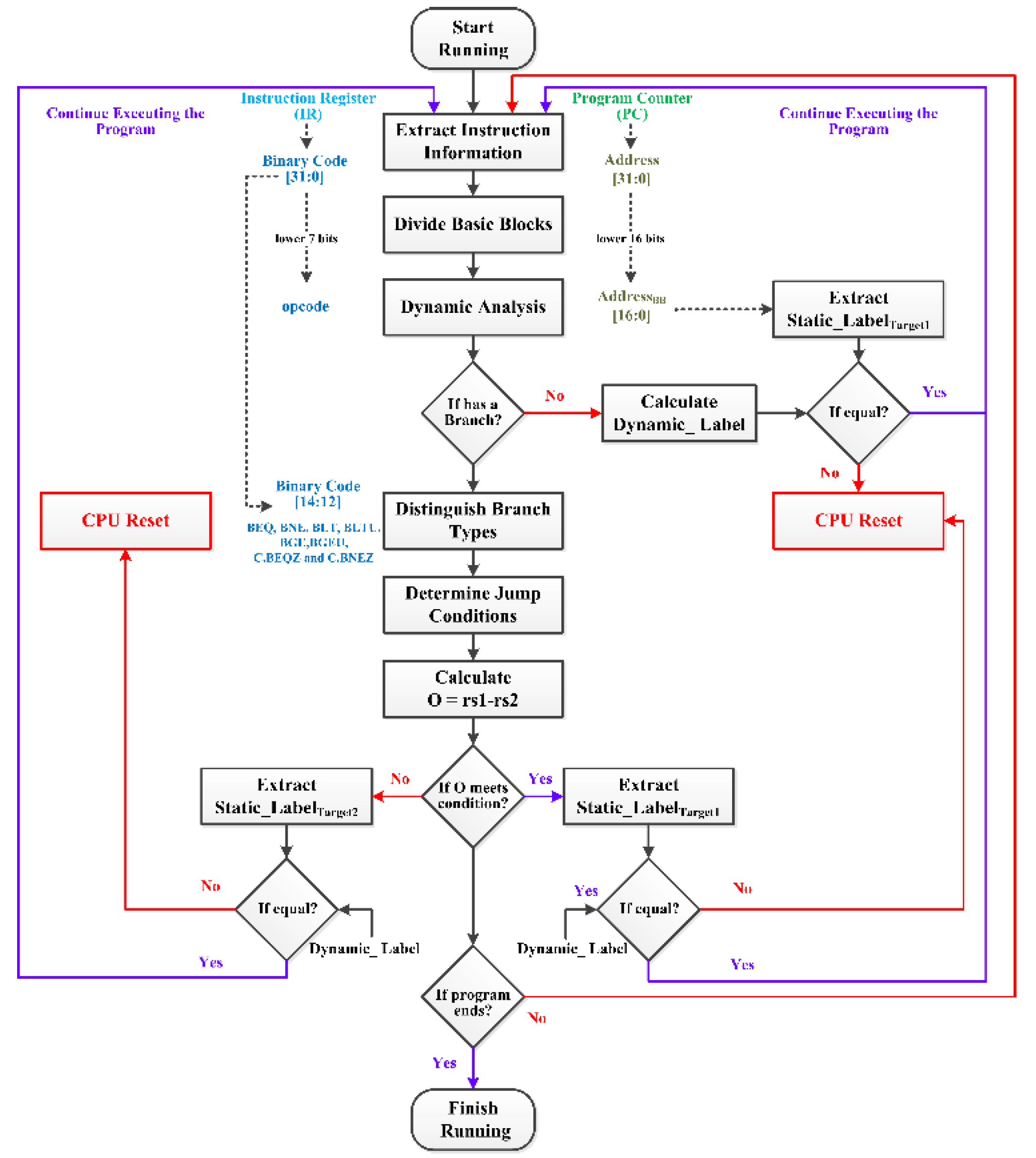
- The control flow integrity protection mechanism based on branch labels is proposed. When the program is offline, generate static labels based on the instruction codes and the jump addresses. When the program runs, the designed hardware security monitoring module will generate dynamic labels according to the same process. If the dynamic and static labels are inconsistent, it is considered that the control flow has been disrupted and the CPU is reset.
2. Related Work
2.1. Prevent Obtaining the Execution Status of Branches
2.2. Encrypt the Branch Information
2.3. Monitor the Integrity of Branch Information
3. Threat Model
3.1. Xuantie E906 Processor
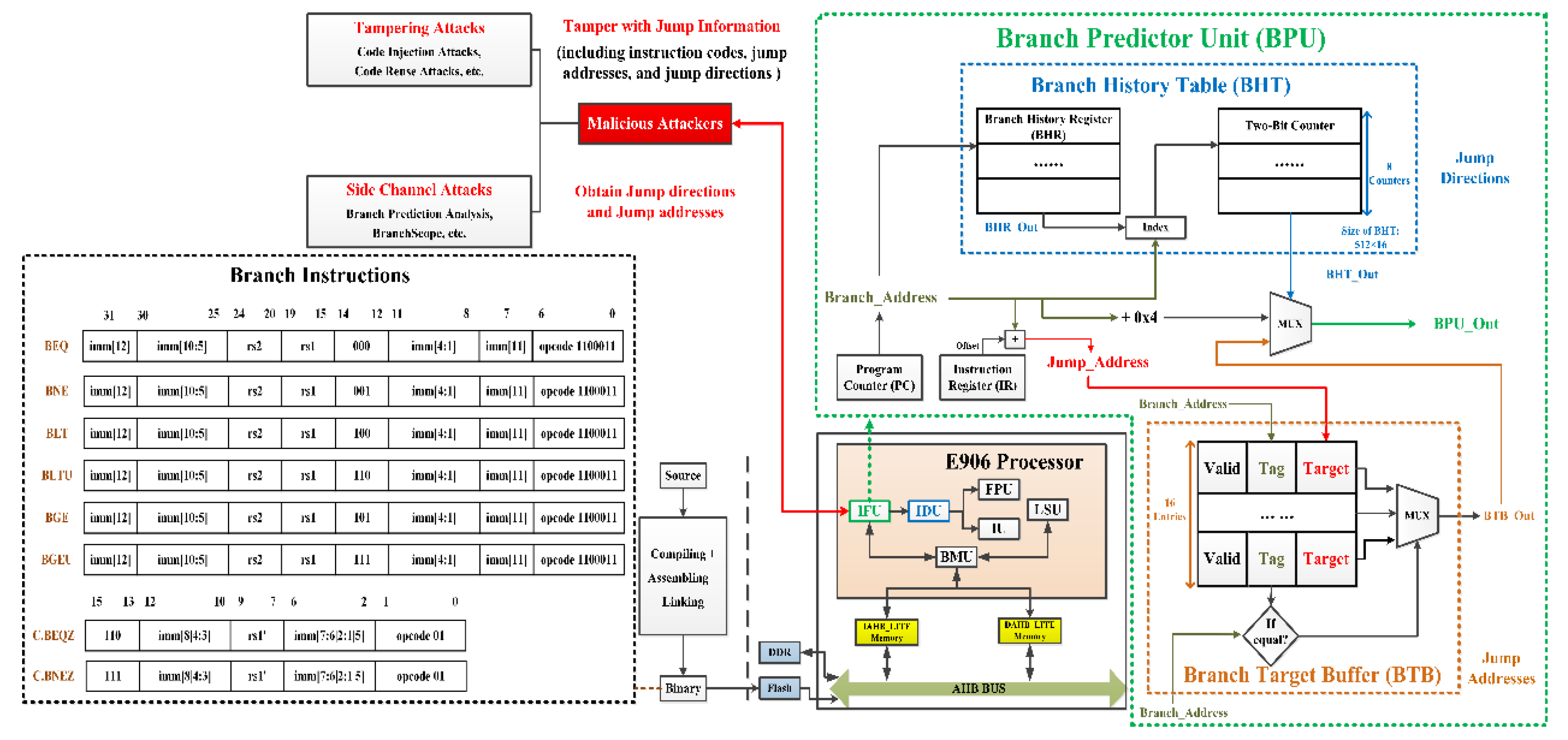
3.2. Branch Prediction Unit
3.3. Security Threats
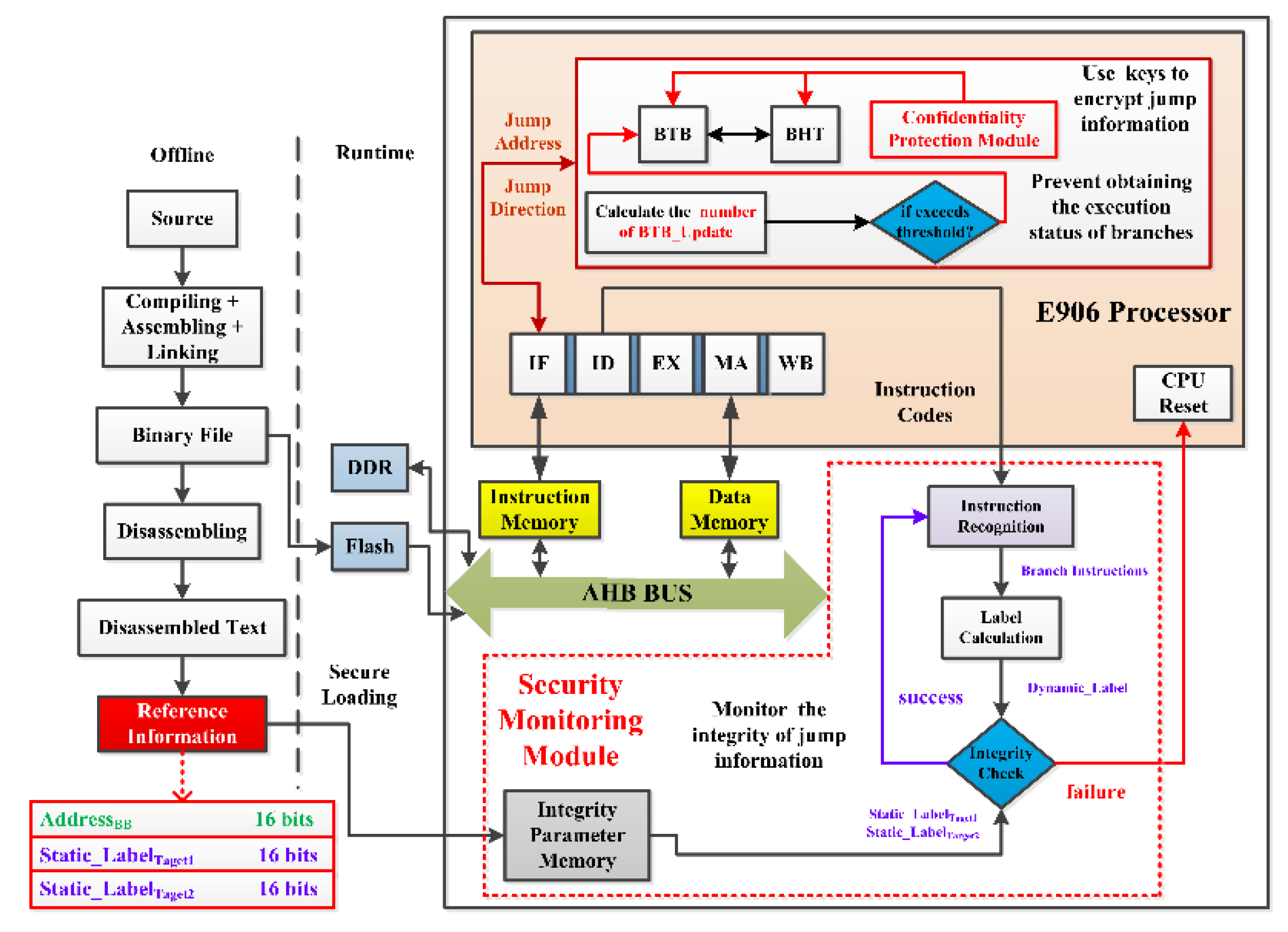
4. The Hardware Security Protection Method for Conditional Branches
4.1. The Branch Information Protection Mechanism Based on Hardware Locking
4.1.1. Identify Characteristics of Attack Behaviors
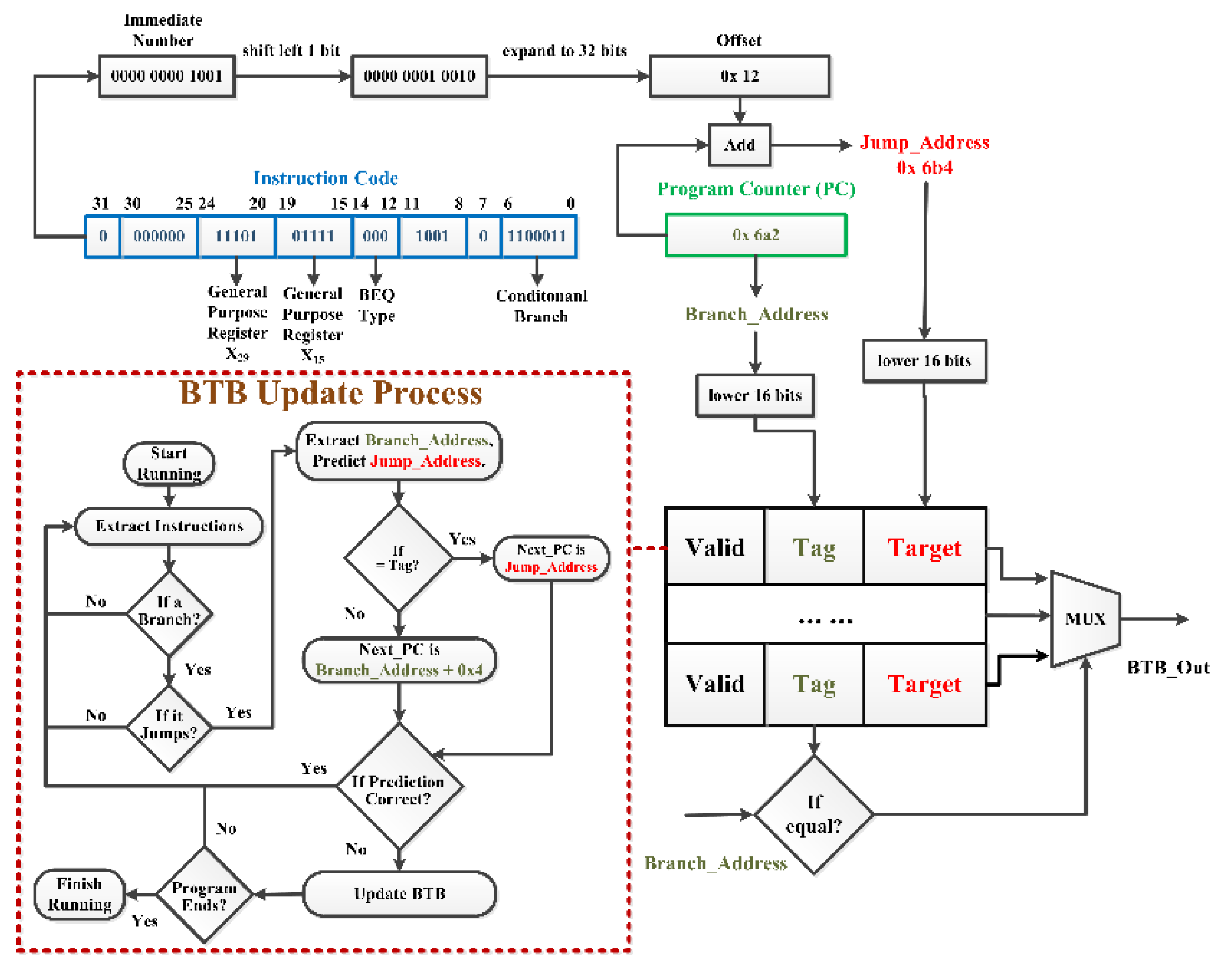
4.1.2. BTB Based on Hardware Locking
4.2. The Branch Information Protection Mechanism Based on Dynamic Isolation
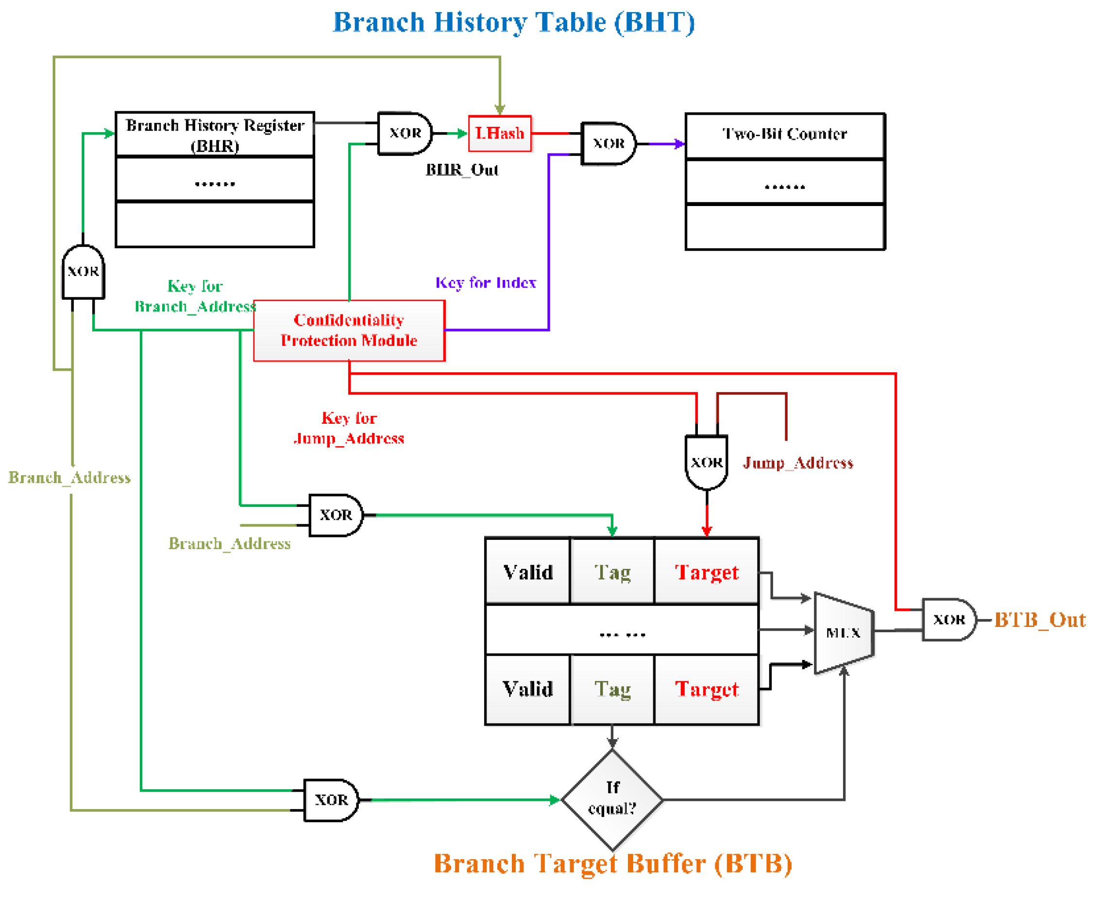
4.2.1. BTB and BHT Based on Dynamic Isolation
4.2.2. The Confidentiality Protection Module
4.3. The Control Flow Integrity Protection Mechanism Based on Branch Labels
4.3.1. Extract the Reference Information
4.3.2. Monitor the Control Flow Integrity
5. Experiments and Results
5.1. Security Analysis
5.1.1. Security of the Hardware Locking Protection Mechanism
5.1.2. Security of the Proposed Hybrid APUF
5.1.3. Security of the Control Flow Integrity Protection Mechanism
5.2. Resource Overhead Assessment
5.3. Performance Overhead Assessment
5.4. Comparison with Other Security Protection Methods
6. Conclusions
Author Contributions
Funding
Data Availability Statement
Acknowledgments
Conflicts of Interest
References
- Arıkan, K.; Palumbo, A.; Cassano, L.; Reviriego, P.; Pontarelli, S.; Bianchi, G.; Ergin, O.; Ottavi, M. Processor Security: Detecting Microarchitectural Attacks via Count-Min Sketches. IEEE Trans. Large Scale Integr. Syst. 2022, 30, 938–951. [Google Scholar] [CrossRef]
- Wang, G.; Chattopadhyay, S.; Gotovchits, I.; Mitra, T.; Roychoudhury, A. oo7: Low-Overhead Defense Against Spectre Attacks via Program Analysis. IEEE Trans. Software Engineering 2021, 47, 2504–2519. [Google Scholar] [CrossRef]
- Zheng, B.; Gu, J.; Wang, J.; Weng, C. CBA-Detector: A Self-Feedback Detector Against Cache-Based Attacks. IEEE Trans. Dependable and Secure Computing 2022, 19, 3231–3243. [Google Scholar] [CrossRef]
- Nasahl, P.; Schilling, R.; Mangard, S. Protecting Indirect Branches Against Fault Attacks Using ARM Pointer Authentication. In Proceedings of the 2021 IEEE International Symposium on Hardware Oriented Security and Trust (HOST), ysons Corner, VA, USA, 12-15 December 2021; pp. 68–79. [Google Scholar]
- Wang, Y.; Wang, Q.; Chen, X.; Chen, D.; Fang, X.; Yin, M.; Zhang, N. ContainerGuard: A Real-Time Attack Detection System in Container-Based Big Data Platform. IEEE Trans. Industrial Informatics 2022, 18, 3327–3336. [Google Scholar] [CrossRef]
- Bhattacharya, S.; Maurice, C.; Bhasin, S.; Mukhopadhyay, D. Branch Prediction Attack on Blinded Scalar Multiplication. IEEE Trans. on Computers 2020, 69, 633–648. [Google Scholar] [CrossRef]
- Islam Chowdhuryy, M. H.; Liu, H.; Yao, F. BranchSpec: Information Leakage Attacks Exploiting Speculative Branch Instruction Executions. In Proceedings of the 2020 IEEE 38th International Conference on Computer Design (ICCD), Hartford, CT, USA, 18-21 October 2020; pp. 529–536. [Google Scholar]
- Le Bon, C.; Rohou, E.; Tronel, F.; Hiet, G. DAMAS: Control-Data Isolation at Runtime through Dynamic Binary Modification. In Proceedings of the 2021 IEEE European Symposium on Security and Privacy Workshops (EuroS&PW), Vienna, Austria, 06-10 September 2021; pp. 86–95. [Google Scholar]
- Kim, S.; Mahmud, F.; Huang, J.; Majumder, P.; Tsai, C.; Muzahid, A.; Kim, E. J. WHISTLE: CPU Abstractions for Hardware and Software Memory Safety Invariants. IEEE Trans. Computers 2023, 72, 811–825. [Google Scholar] [CrossRef]
- Wang, X.; Zhao, Z.; Xu, D.; Zhang, Z.; Hao, Q.; Liu, M. An M-Cache based security monitoring and fault recovery architecture for embedded processor. IEEE Trans. Large Scale Integr. Syst. 2020, 28, 2314–2327. [Google Scholar] [CrossRef]
- Xu, D.; Wang, X.; Hao, Y.; Zhang, Z.; Hao, Q.; Zhou, Z. A More Accurate and Robust Binary Ring-LWE Decryption Scheme and Its Hardware Implementation for IoT Devices. IEEE Trans. Large Scale Integr. Syst. 2022, 30, 1007–1019. [Google Scholar] [CrossRef]
- Xu, D.; Wang, X.; Hao, Y.; Zhang, Z.; Hao, Q.; Jia, H.; Dong, H.; Zhang, L. Ring-ExpLWE: A High-Performance and Lightweight Post-Quantum Encryption Scheme for Resource-Constrained IoT Devices. IEEE Internet of Things J. 2022, 9, 24122–24134. [Google Scholar] [CrossRef]
- Hao, Q.; Zhang, Z.; Xu, D.; Wang, J.; Liu, J.; Zhang, J.; Ma, J.; Wang, X. A Hardware Security-Monitoring Architecture Based on Data Integrity and Control Flow Integrity for Embedded Systems. Appl. Sci. 2022, 12, 7750. [Google Scholar] [CrossRef]
- Wang, X.; Zhang, Z.; Hao, Q.; Xu, D.; Wang, J.; Jia, H.; Zhou, Z. Hardware-Assisted Security Monitoring Unit for Real-Time Ensuring Secure Instruction Execution and Data Processing in Embedded Systems. Micromachines 2021, 12, 1450. [Google Scholar] [CrossRef] [PubMed]
- Zhao, L.; Li, P.; Hou, R.; Huang, M. C.; Liu, P.; Zha, L.; Meng, D. Exploiting Security Dependence for Conditional Speculation Against Spectre Attacks. IEEE Trans. Computers 2021, 70, 963–978. [Google Scholar] [CrossRef]
- Zhao, L.; Li, P.; Hou, R.; Huang, M. C.; Li, J.; Zhang, L.; Qian, X.; Meng, D. A Lightweight Isolation Mechanism for Secure Branch Predictors. In Proceedings of the 2021 58th ACM/IEEE Design Automation Conference (DAC), San Francisco, CA, USA, 05-09 December 2021; pp. 1267–1272. [Google Scholar]
- Koruyeh, E. M.; Haji Amin Shirazi, S.; Khasawneh, K. N.; Song, C.; Abu-Ghazaleh, N. SpecCFI: Mitigating Spectre Attacks using CFI Informed Speculation. In Proceedings of the 2020 IEEE Symposium on Security and Privacy (SP), San Francisco, CA, USA, 18-21 May 2020; pp. 39–53. [Google Scholar]
- Zhang, J.; Qi, B.; Qin, Z.; Qu, G. HCIC: Hardware-assisted Control-flow Integrity Checking. IEEE Internet Things J. 2018, 6, 458–471. [Google Scholar] [CrossRef]
- Hao, Q.; Xu, D.; Zhang, Z.; Wang, J.; Le, T.; Wang, J.; Zhang, J.; Liu, J.; Ma, J.; Wang, X. A Hardware-Assisted Security Monitoring Method for Jump Instruction and Jump Address in Embedded Systems. In Proceedings of the 2022 8th Annual International Conference on Network and Information Systems for Computers (ICNISC), Hangzhou, China, 16-19 September 2022; pp. 197–202. [Google Scholar]
- Shi, J.; Lu, Y.; Zhang, J. Approximation Attacks on Strong PUFs. IEEE Trans. Computer-Aided Design of Integrated Circuits and Systems 2019, 39, 2138–2151. [Google Scholar] [CrossRef]
- Tan, Y.; Wei, J.; Guo, W. The Micro-architectural Support Countermeasures against the Branch Prediction Analysis Attack. In Proceedings of the 2014 IEEE 13th International Conference on Trust, Security and Privacy in Computing and Communications, Beijing, China, 24-26 September 2014; pp. 276–283. [Google Scholar]
- Evtyushkin, D.; Riley, R.; Abu-Ghazaleh, N.; Ponomarev, D. BranchScope: A New Side-Channel Attack on Directional Branch Predictor. ACM SIGPLAN Notices 2018, 53, 693–707. [Google Scholar] [CrossRef]
- Li, P.; Zhao, L.; Hou, R.; Zhang, L.; Meng, D. Conditional Speculation: An Effective Approach to Safeguard Out-of-Order Execution Against Spectre Attacks. In Proceedings of the 2019 IEEE International Symposium on High Performance Computer Architecture (HPCA), Washington, DC, USA, 16-20 February 2019; pp. 264–276. [Google Scholar]
- Vougioukas, I.; Nikoleris, N.; Sandberg, A.; Diestelhorst, S.; Al-Hashimi, B. M.; Merrett, G. V. BRB: Mitigating Branch Predictor Side-Channels. In Proceedings of the 2019 IEEE International Symposium on High Performance Computer Architecture (HPCA), Washington, DC, USA, 16-20 February 2019; pp. 466–477. [Google Scholar]
- Zhang, Z.; Wang, X.; Hao, Q.; Xu, D.; Zhang, J.; Liu, J.; Ma, J. High-Efficiency Parallel Cryptographic Accelerator for Real-Time Guaranteeing Dynamic Data Security in Embedded Systems. Micromachines 2021, 12, 560. [Google Scholar] [CrossRef] [PubMed]
- Bahar Talukder, B. M. S.; Ferdaus, F.; Rahman, M. T. Memory-Based PUFs are Vulnerable as Well: A Non-Invasive Attack Against SRAM PUFs. IEEE Trans. on Information Forensics and Security 2021, 16, 4035–4049. [Google Scholar] [CrossRef]
- Ge, L.; Parhi, K. K. Molecular MUX-Based Physical Unclonable Functions. In Proceedings of the 2020 IEEE Computer Society Annual Symposium on VLSI (ISVLSI), Limassol, Cyprus, 06-08 July 2020; pp. 482–487. [Google Scholar]
- Hamza, M. A.; Issa, H. H.; Eisa, S. FPGA-Based Modified Ring Oscillator Physical Unclonable Function for Internet of Vehicles. In Proceedings of the 2023 40th National Radio Science Conference (NRSC), Giza, Egypt, 30 May 2023 - 01 June 2023; pp. 208–216. [Google Scholar]
- Alkatheiri, M. S.; Zhuang, Y. Towards fast and accurate machine learning attacks of feed-forward arbiter PUFs. In Proceedings of the 2017 IEEE Conference on Dependable and Secure Computing, Taipei, Taiwan, 07-10 August 2017; pp. 181–187. [Google Scholar]
- Avvaru, S. V. S.; Zeng, Z.; Parhi, K. K. Homogeneous and Heterogeneous Feed-Forward XOR Physical Unclonable Functions. IEEE Trans. Information Forensics and Security 2020, 15, 2485–2498. [Google Scholar] [CrossRef]
- Maes, R.; Herrewege, A. V.; Verbauwhede, I. PUFKY: A Fully Functional PUF-Based Cryptographic Key Generator. In Proceedings of the Cryptographic Hardware and Embedded Systems -- CHES 2012, Leuven, Belgium, 9-12 September 2012; pp. 302–319. [Google Scholar]
- Wang, X.; Wang, W.; Xu, B.; Du, P. A fine-grained hardware security approach for runtime code integrity in embedded systems. J. Univers. Comput. Sci. 2018, 24, 515–536. [Google Scholar]
- Wu, W.; Wu, S.; Zhang, L.; Zou, J.; Dong, L. LHash: A lightweight hash function. In Proceedings of the Springer International Conference on Information Security and Cryptology, Guangzhou, China, 27–30 November 2013; pp. 291–308. [Google Scholar]
- T-head-Semi/opene906. Available online: https://github.com/T-head-Semi/opene906 (accessed on 18 October 2021).
- M, I.; Kaur, M.; Raj, M.; R, S.; Lee, H.-N. Cross Channel Scripting and Code Injection Attacks on Web and Cloud-Based Applications: A Comprehensive Review. Sensors 2022, 22, 1959. [Google Scholar] [CrossRef] [PubMed]
- Salehi, M.; Hughes, D.; Crispo, B. MicroGuard: Securing Bare-Metal Microcontrollers against Code-Reuse Attacks. In Proceedings of the 2019 IEEE Conference on Dependable and Secure Computing (DSC), Hangzhou, China, 18-20 November 2019; pp. 1–8. [Google Scholar]
- Xu, C.; Zhang, L.; Law, M. -K.; Zhao, X.; Mak, P. -I.; Martins, R. P. Modeling Attack Resistant Strong PUF Exploiting Stagewise Obfuscated Interconnections With Improved Reliability. IEEE Internet of Things J. 2023, 10, 16300–16315. [Google Scholar] [CrossRef]
- Alamro, M. A.; Zhuang, Y.; Aseeri, A. O.; Alkatheiri, M. S. Examination of Double Arbiter PUFs on Security against Machine Learning Attacks. In Proceedings of the 2019 IEEE International Conference on Big Data (Big Data), Los Angeles, CA, USA, 09-12 December 2019; pp. 3165–3171. [Google Scholar]

| Benchmarks | Proportion of Branches in All Instructions |
Occupancy Rate of BTB | Max Number of BTB_Update |
|---|---|---|---|
| hello_world | 12.54% | 37.5% | 6 |
| coremark | 15.41% | 100% | 8 |
| basicmath | 12.52% | 37.5% | 2 |
| SHA1 | 13.07% | 37.5% | 3 |
| FFT | 13.60% | 62.5% | 5 |
| bitcount | 13.15% | 50% | 3 |
| CRC16 | 13.23% | 37.5% | 3 |
| patricia | 13.04% | 87.5% | 7 |
| quicksort | 13.22% | 62.5% | 5 |
| blowfish | 13.21% | 25% | 3 |
| NumFF | Stability | Accuracy 1 | Resource 2 |
|---|---|---|---|
| 2 | 95.1% | 58.8% | 209 |
| 4 | 98.8% | 53.3% | 217 |
| 8 | 92.5% | 60.1% | 233 |
| 16 | 82.3% | 64.9% | 265 |
| Benchmarks | Attack Success Rate | |
|---|---|---|
| Without Protection | With Hardware Locking BTB | |
| hello_world | 98.1% | 58.3% |
| coremark | 97.4% | 59.6% |
| basicmath | 97.9% | 56.4% |
| SHA1 | 97.6% | 57.5% |
| FFT | 98.3% | 58.1% |
| bitcount | 97.3% | 59.4% |
| CRC16 | 97.5% | 58.7% |
| patricia | 98.8% | 57.9% |
| quicksort | 98.6% | 58.3% |
| blowfish | 98.5% | 55.9% |
| APUF Types | Stability | Randomness | Uniqueness | Accuracy | ||
|---|---|---|---|---|---|---|
| CMA-ES | LR | ANN | ||||
| Traditional APUF | 98.85% | 51.31% | 49.57% | 98.28% | 99.31% | 99.27% |
| 2XOR-APUF | 98.83% | 48.89% | 49.65% | 95.18% | 97.32% | 96.98% |
| DAPUF | 98.81% | 49.63% | 50.11% | 64.84% | 65.65% | 75.16% |
| FF-APUF | 97.84 | 50.58% | 48.91% | 86.13% | 87.65% | 88.01% |
| Hybrid APUF | 98.79% | 49.85% | 50.06% | 53.32% | 56.78% | 57.93% |
| Benchmarks | Attacks on Conditional Branches | Attacks on Unconditional Jumps | |||
|---|---|---|---|---|---|
| Instruction Codes | Jump Addresses |
Jump Directions |
Instruction Codes | Jump Addresses | |
| hello_world | 100% | 100% | 100% | 100% | 93.4% |
| coremark | 100% | 100% | 100% | 100% | 92.2% |
| basicmath | 100% | 100% | 100% | 100% | 95.7% |
| SHA1 | 100% | 100% | 100% | 100% | 96.3% |
| FFT | 100% | 100% | 100% | 100% | 96.4% |
| bitcount | 100% | 100% | 100% | 100% | 94.3% |
| CRC16 | 100% | 100% | 100% | 100% | 95.4% |
| patricia | 100% | 100% | 100% | 100% | 96.8% |
| quicksort | 100% | 100% | 100% | 100% | 96.1% |
| blowfish | 100% | 100% | 100% | 100% | 93.6% |
| Circuits | LUTs | Flip Flops | Slices |
|---|---|---|---|
| Traditional APUF | 409 | 156 | 133 |
| 2XOR-APUF | 672 | 165 | 223 |
| DAPUF | 687 | 165 | 228 |
| FF-APUF | 429 | 150 | 142 |
| Hybrid APUF | 712 | 168 | 231 |
| Benchmarks | With Proposed Method | Without Proposed Method | Performance Overhead |
|---|---|---|---|
| hello_world | 1.28 | 1.24 | 4.03% |
| coremark | 3.38 | 3.21 | 5.30% |
| basicmath | 2.37 | 2.28 | 3.95% |
| SHA1 | 2.07 | 1.98 | 4.55% |
| FFT | 2.51 | 2.39 | 5.02% |
| bitcount | 1.42 | 1.36 | 4.41% |
| CRC16 | 1.65 | 1.58 | 4.43% |
| patricia | 1.55 | 1.47 | 5.44% |
| quicksort | 1.83 | 1.76 | 3.98% |
| blowfish | 3.51 | 3.35 | 4.78% |
| Methods | Prevent Obtaining Execution Status of Branches | Encrypt Branch Information |
Monitoring the CFI | Resource Overhead |
Performance Overhead |
|---|---|---|---|---|---|
| Conditional Speculation [15] |
Yes | No | No | About 1.52 KB | The average is 2.8%, but in extreme cases it may approach 30%. |
| Secure Branch Predictor [16] |
Yes | Yes | No | BTB_Area increased by 0.24%, PHT_Area increased by 0.11%. | The average is a few percent, but sometimes it may be more than 20%. |
| Countermeasure against BPA [21] | Yes | No | No | Area increased by 8KB | 0.12% |
| HCIC [18] | No | Yes | Yes | Binary_Size increasd by 0.78%. | 0.95% |
| M-Cache based Security Monitor [10] |
No | No | Yes | Area increased by 20.99%. | 9.33% |
| Hardware Monitoring Module [13] | No | No | Yes | Consumed 486 Slices and 1374 LUTs. | Less than 9.52% |
| The Propose Method | Yes | Yes | Yes | Consumed 613 Slices and 1851 LUTs. | Less than 5.5% |
Disclaimer/Publisher’s Note: The statements, opinions and data contained in all publications are solely those of the individual author(s) and contributor(s) and not of MDPI and/or the editor(s). MDPI and/or the editor(s) disclaim responsibility for any injury to people or property resulting from any ideas, methods, instructions or products referred to in the content. |
© 2024 by the authors. Licensee MDPI, Basel, Switzerland. This article is an open access article distributed under the terms and conditions of the Creative Commons Attribution (CC BY) license (http://creativecommons.org/licenses/by/4.0/).


