Preprint
Article

A Novel Five-Surface Phosphor-in-Ceramic for High Illumination and Excellent Color Uniformity in Larger Scale LEDs

Altmetrics

Downloads

79

Views

52

Comments

0

Submitted:

25 April 2024

Posted:

28 April 2024

You are already at the latest version

Alerts
Abstract
A novel five-surface phosphor-in-ceramic (FS-PiC) for high illumination and excellent color uniformity in larger-scale LEDs for sensor light source application is demonstrated. YAG phosphor (Y3Al5O12:Ce3+) was uniformly mixed with ceramic and sintered at 680°C to form a phosphor wafer. A sophisticated laser engraving was employed on the phosphor wafer to form a saddle-shaped large-scale FS-PiC LEDs. The performance of the FS-PiC LEDs exhibited the illumination of 401lm, average color temperature (CCT) of 5488K±110K, and color coordinates (CIE) of (0.3179±0.003, 0.3352±0.003). In contrast to convention single-surface phosphor-in-ceramic (SS-PiC) LEDs, the performance exhibited the illumination of 380lm, average CCT of 5830K±758K, and CIE of (0.3083±0.07, 0.3172±0.07). These indicated that the performance of the FS-PiC LEDs was higher than the SS-PiC LEDs for illumination, CCT, and CIE of 1.1, 7, and 23 times, respectively. Furthermore, the FS-PiC LEDs demonstrate lower lumen loss of 2% and less chromaticity shift of 5.4x10⁻³ under accelerated aging at 350°C for 1008 hours, owing to the high ceramic melting temperature of up to 510°C. In this study, the proposed FS-PiC larger-scale LEDs having excellent optical performance and high reliability may be the promising candidates to replace the convention phosphor-in-organic silicone material used in high-power LEDs for the next generation of sensor light sources, display, and headlight applications.
Keywords: 
Subject: Engineering  -   Electrical and Electronic Engineering

1. Introduction

White light-emitting diodes (LEDs) are essential because they can replace traditional light sources, such as incandescent and fluorescent lamps, due to their high luminous efficiency, long lifetime, and environmental friendliness [1,2]. One major challenge in white LED technology is achieving high color uniformity and better reliability, which is critical for high-power lighting applications. There are some essential approaches to attain high color uniformity in white LEDs. One uses the scattering effect to deflect the light direction to balance blue and yellow light distributions by introducing micro- and nano-particles/structures and optimizing the phosphor particle size [3,4,5,6]. The other uses the Beer-Lambert law to adjust the amount of blue light at specific angles by optimizing the thickness distribution, location, and material of phosphor-converted layers [7,8,9,10]. However, there are still limited technologies for achieving high color uniformity (CCT and CIE) and good reliability in large-scale white LEDs. Therefore, it is essential to develop a suitable large-scale white LED package to achieve high color uniformity with excellent reliability.
Furthermore, low light extraction efficiency (LEE) of the LED modules has been an important issue. This is due to the total internal reflection (TIR) effect [11] on the top encapsulation surface of traditional modules, which reduces light emission and leads to the conversion of captured light rays into heat. Researchers have recently developed various methods to reduce TIR and enhance LEE. These include nano/micro-scale surface structures [12], microlens arrays [13], and precision mechanical engraving structures [14]. However, the nano/micro-scale approaches may be costly. The microlens arrays may also suffer from optical dispersion and material issues affecting uniformity and damage, while precision mechanical engraving is limited to millimeter-scale sizes due to equipment constraints. Laser engraving approach is a promising technology for creating microstructures on ceramic phosphor plates without contact or chemical agents to achieve high accuracy, small dimensions, and the ability to shape and pattern as desired geometry. In laser engraving, the pulsed picosecond lasers enable to adjust processing depth through power modulation and processing area through beam diameter adjustment to create intricate patterns.
The primary preparation for process chip-scaled package white light-emitting diode (CSP-LED) is as follow. The CSP-LED processes involve two parts: pressing chip arrays with yellow phosphor-in-organic silicone material (PiOS) and cutting them into a single LED. The substrate prepares LED chips and then applies colloids before placing the yellow PiOS material sheet on the chip. Simultaneous hot pressing combines the phosphors on the chips. The resulting wafer is cut into single LEDs. There are many defects in the pressing process with the PiOS, such as poor uniformity of luminous intensity, uneven heat transfer, poor color temperature consistency. The poor thermal stability of the PiOS may be due to the lower silicon transition temperature of 150°C. These defects can lead to a lower product rate, short life, etiolation, and apertures with noticeable brightness differences in the lighting range.
Regarding packaging structure, there is directly attached to the chip surface and has the advantage of achieving high color uniformity through its sufficient scattering ability and uniform thickness distribution. The manufacturing methods were pulse jetting [15], dispensing [16], or compression molding [8] to control the top thickness of the encapsulant, forming chip-scale packaging (CSP) structures. These CSP structures have the potential to achieve both a small size and a high luminous density.
In this study, we propose a novel FS-PiC for high illumination and excellent color uniformity in larger-scale LEDs for sensor light source application. The FS-PiC structure is the CSP-LEDs. The structure utilizes a pentahedron to cover the LED light source, enhancing the contact between the light source and the effective phosphor area compared to a flat surface. Moreover, it allows for controlling the light emission angle to concentrate the light more effectively. YAG phosphor (Y3Al5O12:Ce3+) was uniformly mixed with glass matrix powder and sintered at 680°C to form a PiC wafer. The laser engraving was employed to manufacture a saddle-shaped FS-PiC structure on the surface of LED wafer. Then, we packaged the saddle-shaped FS-PiC with the LED flip chip—the experiment aimed to create a micro-square via structure on the ceramic phosphor plates by laser ablation. We expect the micro-square via structure to enhance the ceramic phosphor plates' light extraction and scattering properties, thereby improving their luminous performance.
The FS-PiC-based white LEDs demonstrate a lumen loss of only 2% and less chromaticity shift of 5.4x10⁻³ under accelerated aging at 350°C for 1008 hours, owing to the high ceramic melting temperature of up to 510°C. Unlike convention conformal package structures, the top and side thickness of FS-PiC are controllable and show only a 0.01% CCT shift at 6000 K, which has excellent potential to achieve high color uniformity. The proposed FS-PiC larger-scale LEDs with excellent optical performance and high reliability may be promising candidates to replace the convention phosphor-in-organic silicone material used in high-power LEDs for the next generation of sensor light sources, display, and headlight applications.

2. Fabrication

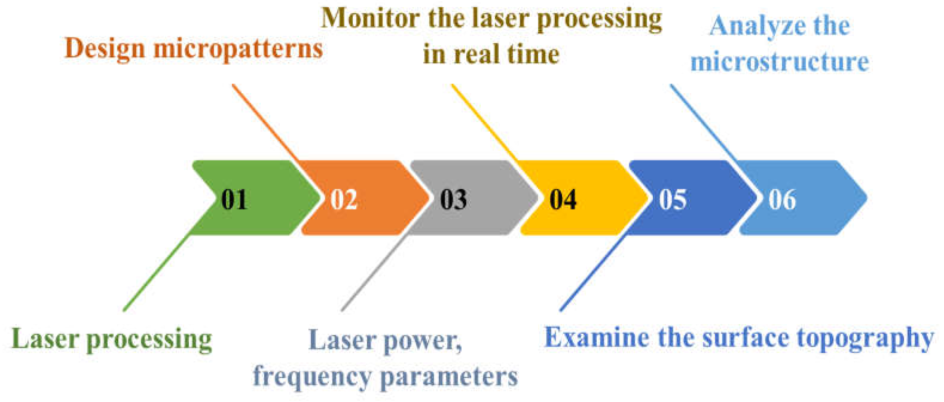
The fabrication process of the FS-PiC structure for the CSP-LED involves several critical steps. First, achieving uniform mixing of the phosphors with the ceramic powder by optimizing the mixing time, temperature, and pressure is crucial. Second, the sintering temperature and time are essential for forming the PiC wafer, as they affect the densification and homogeneity of the phosphor-ceramic composite. Third, the laser processing parameters, such as laser power, scanning speed, and pulse frequency, need to be carefully controlled to ensure the formation of a uniform and precise saddle-shaped FS-PiC structure. Finally, optimize the packaging process for an excellent thermal and mechanical connection between the FS-PiC and the LED flip chip.
The compositions of the glass matrix were B2O3, Sb2O3, SiO2, and Ta2O5. The mixed raw materials were melted at 557°C. After cooling, we ground the glass matrix of the B2O3-Sb2O3-SiO2-Ta2O5 (D263, Schott AG, Jena, Germany) into ceramic powders with a size of about 10-μm. Next, we uniformly spread the yellow phosphors (Y3Al5O12:Ce3+, NYAG4454, Intematrix Corp., Fremont, California, U.S.A) with a size of about 15 μm into the glass matrix powder with a weight ratio of 84wt%. Table 1 lists fabrication parameters. The average powder size distribution was 0.34 um, as shown in Figure 1, which the material was mixed with a tubular vibration mixer for 4 hours at 450 rpm. We then pressed the mixture powder to form a PiC precursor. Then, a 4-inch PiC powder block was produced and sintered at 680°C for 30 minutes and annealed at 350°C for 120 minutes below the glass transition temperature in a ceramic die-casting furnace. In the cutting and grinding process depicted in Fugure 2, we controlled the thickness and diameter of the PiC wafer to be 0.3 mm and 90 mm, respectively.
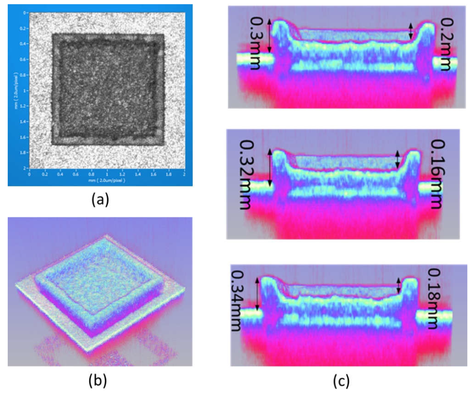
Laser engraving was employed to create precise micro-patterns on phosphor films within PiC wafers. A UV picosecond laser screw-feed processing was used to modify the PiC wafer surface. Then, we manufactured a saddle-shaped FS-PiC structure through high-temperature annealing and acid-etching processes. We adjusted parameters such as laser power, frequency, and focus throughout fabrication to achieve the desired FS-PiC structure on the PiC wafer. These experimental parameters significantly affected the material removal rate, surface quality, and morphology of the FS-PiC structures. Laser power was crucial in controlling the material removal rate and depth. While higher power facilitated more significant material removal, it also posed the risk of thermal damage and micro-cracks. Therefore, optimizing the laser power was necessary to ensure the quality of the FS-PiC structure. Laser frequency, however, influenced the size and shape of the FS-PiC structures. Determining the optimal frequency was vital to achieving the desired microporous structure. During the laser engraving process, we needed to consider bottom flatness, opening chipping, and processing slope, as shown in Fugure 3. The laser engraving processing parameters are 44W laser energy, 1.3m/s scanning speed, and 33s processing time, more detail parameters, as listed in Table 2. Figure 4 shows each fabricated saddle-shaped FS-PiC structure with an inside/outside width of 1.25/1.5 mm and a depth of 0.2 mm, respectively, which would fit the LED chip size of 45-mil. We used an optical coherence tomography device (IVS-2000-HR, Santec, Japan) to measure the information about the surface roughness, uniformity, and topographical characteristics of the PiC layer, as shown in Fugure 4(c). These images can reveal grain size, particle distribution, and surface texture, visually representing the phosphor layer's morphology. Because of the rough surface of the saddle-shaped FS-PiC structure, it was difficult to bond with the LED chip. The secondary annealing improved the surface roughness of this microstructure, as reported [22]. In this study, the saddle-shaped FS-PiC structure was annealed in air for 12 hours at temperatures of 300°C to smooth the inside of the structure surface.
Figure 3. Schematic diagram of laser screw-feed processing.
Preprints 104826 g003
Epoxy curing was used to create the white CSP-LEDs for the package between the prepared saddle-shaped FS-PiGs and the blue LEDs. The CSP-LED is necessary to ensure alignment, adhesive dispensing parameters, and uniform coating during packaging. The FS-PiC chip was bonded by a controlled pressure using an X-Y axis platform, adjusting pressure and temperature settings. The following steps are outline the detailed implementation process:
Step 1:
Positioning each FS-PiC structure and the blue LED array with the substrate ensures the surface is clean and dust-free to prepare the CSP.
Step 2:
Utilize a dispenser to apply translucent epoxy glue on each blue LED to ensure precise control of the glue's amount and placement.
Step 3:
The FS-PiC structure can be picked up using the vacuum nozzle and then transferred to the appropriate position before being placed onto the blue LED. Then, the pressing machine forms a sealed cavity between itself and the platform of the operating table, and it pumps the cavity into a vacuum, with a vacuum degree ranging from -95 to 100 kPa.
Step 4:
We controlled a fixed pressure of 20-30 kgf/cm2 and pressed for 5-10 mins with the pressing platform.
Step 5:
We put the blue LED-covered FS-PiC chip into the oven for sintering and curing to enable the adhesive to solidify. We maintain the sintering temperature at 150°C, usually taking about 2 hours. To achieve complete curing of the epoxy resin, we control the curing temperature at 120°C for 4 hours, as shown in Fugure 5.
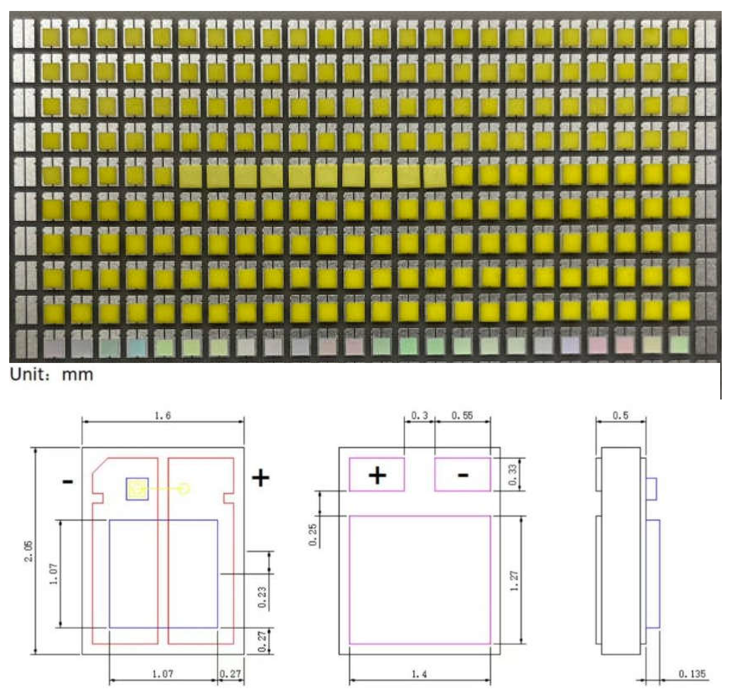
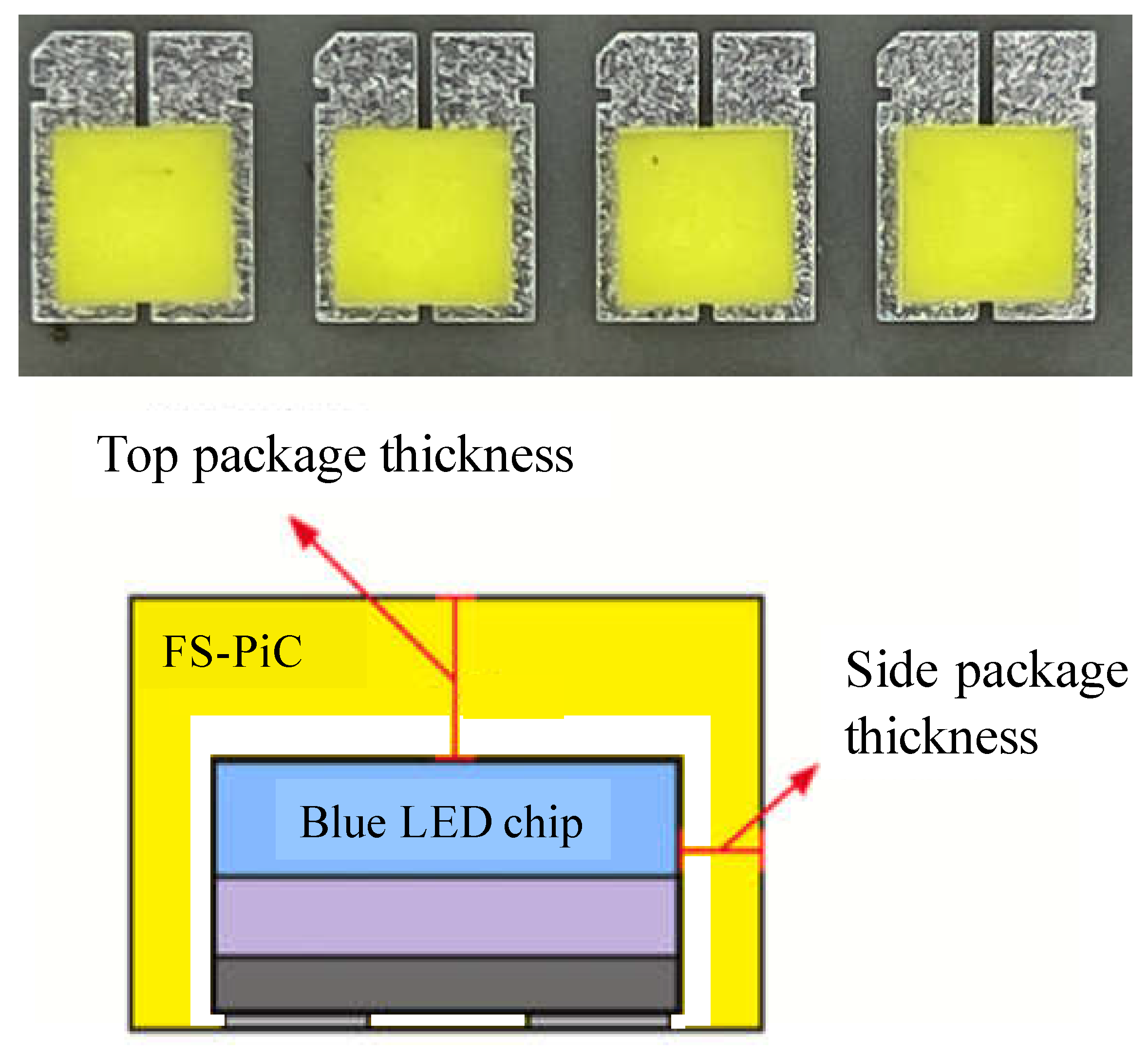
The abovementioned methods could be used to package the chip, emitting light through five chip surfaces. The top and side surface thickness are 100 μm and 125 μm, respectively. The saddle-shaped FS-PiG thickness of the four sides of one chip are the same. Figure 6 shows the CSP-LED with FS-PiG on the substrate, which is just for testing some light performance more conveniently.

3. Results and Discussion

3.1. Analysis of the Laser Processing

In this study, ceramic phosphors based on Y3Al5O12:Ce3+ were prepared by heated press sintering method [17]. We investigated their photoluminescence properties and performance as converters for high color rendering index warm white LEDs. To evaluate the optical and thermal properties of the FS-PiC-based white LEDs, we measured their luminous flux, color temperature, and chromaticity coordinates at different operating currents. In addition, we performed accelerated aging tests on the LEDs to investigate their reliability under high-temperature conditions. The experimental results have shown that these parameters produce a high-quality structure with precise and uniform features, which can provide excellent thermal conductivity and package properties for CSP packaging.
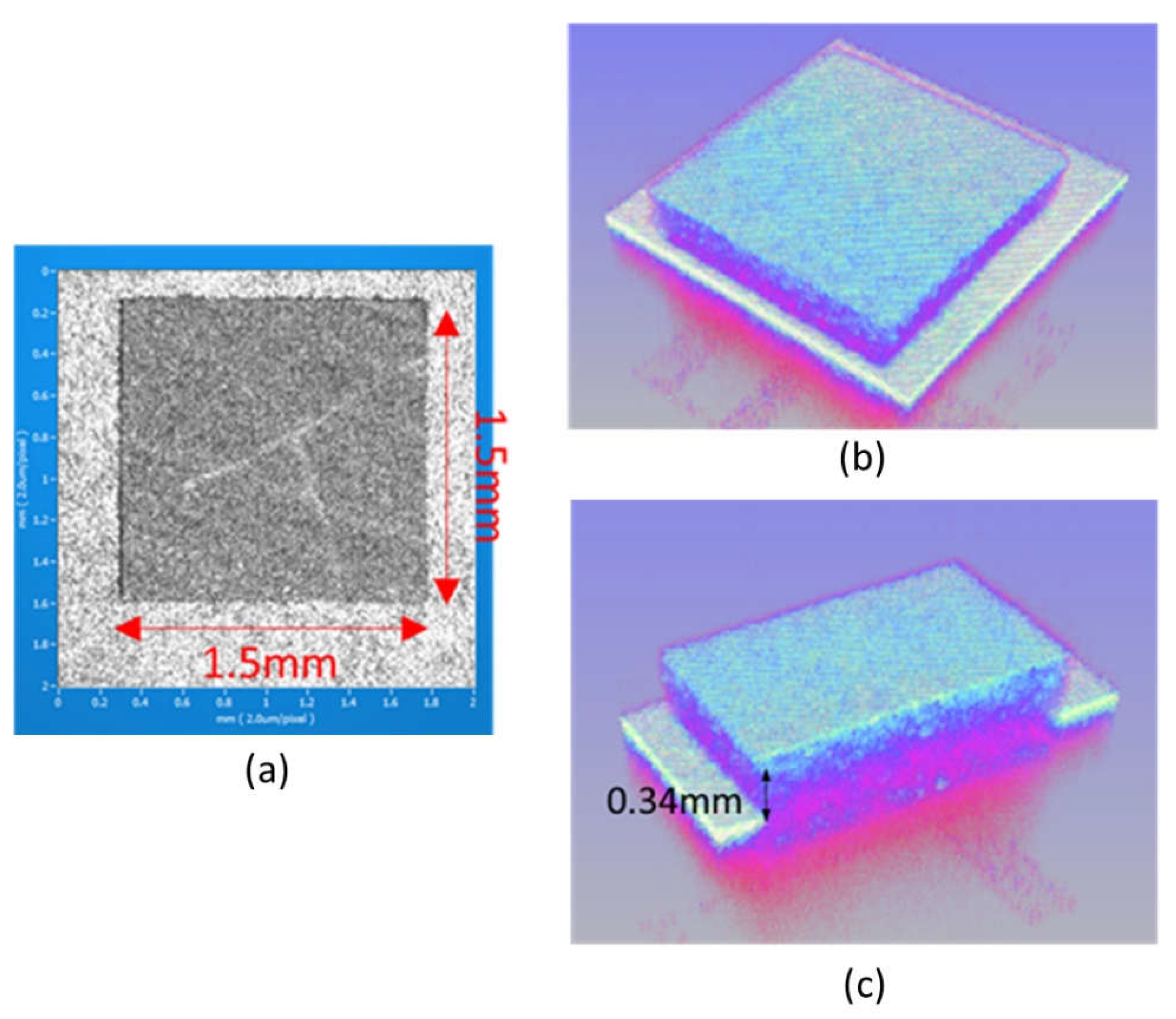
These techniques provide valuable information about the surface roughness, uniformity, and topographical characteristics of the phosphor layer, as shown in Figure 7 and Figure 8. The images can reveal grain size, particle distribution, and surface texture, visually representing the phosphor layer's morphology. We performed the laser engraving process on the surface of a five-layer phosphor layer. We achieved a depth of 13.2 mm with the laser, creating a precise laser micro via structure with a diameter of 1.8 mm, as shown in Figure 8 (c). The laser engraving resulted in a well-defined and controlled surface morphology on the phosphor layer. The deep laser engraving reached a depth of 13.2 mm, allowing for the creation of intricate patterns and structures within the phosphor layer. This deep laser machining capability opens up possibilities for various applications that require precise and profound modifications within the phosphor layer.
Additionally, the laser engraving created during the process had a diameter of 1.8 mm. These laser micro via structure serve as channels or pathways for light propagation within the phosphor layer. The precise and controlled formation of these micro via structure ensures efficient light transmission and distribution, contributing to the overall performance of the phosphor layer.

3.2. Optical Characterization

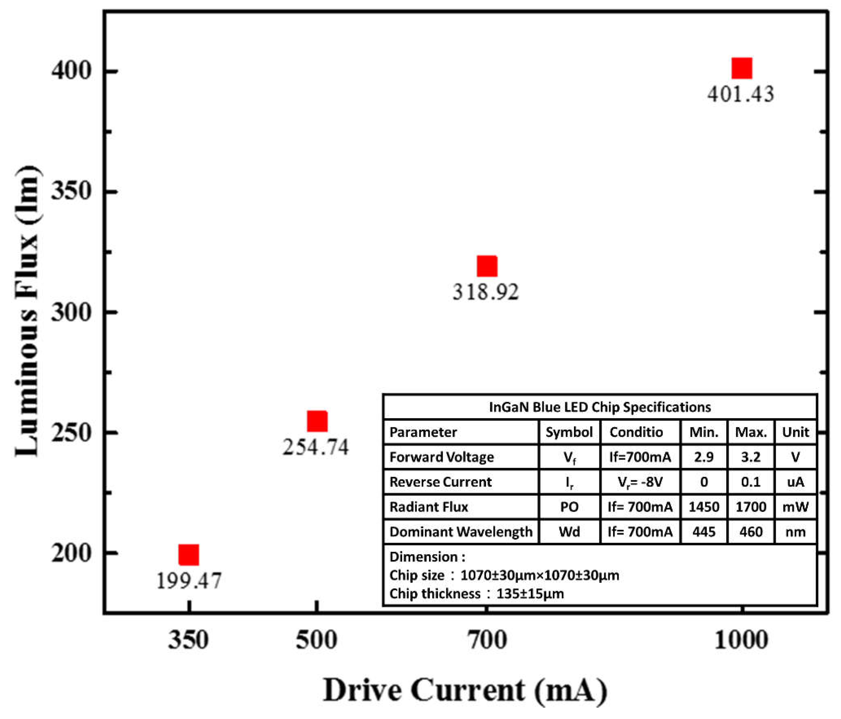
The luminous flux of the FS-PiC-based white CSP-LEDs was measured by using an integrating sphere system (LMS-8000, Radiant) at different driving currents ranging from 350 mA to 1000 mA, as shown in Fugure 9. The luminous flux of the LEDs increases with increasing driving current. At a driving current of 1000 mA, the device achieves a maximum luminous flux of 401 lm. The maximum luminous flux of FS-PiG was 1.05 times larger than SS-PiG when the maximum luminous flux of SS-PiG was 380lm.
The color temperature and chromaticity coordinates of the FS-PiC-based white CSP-LEDs were measured using a spectroradiometer (CAS 140CT, Instrument Systems) equipped with an integrating sphere (IS-1.5-SA, Instrument Systems) at different driving currents. The color temperature of the LEDs increases from 5638 K to 5935 K as the driving current increases from 350 mA to 1000 mA. The chromaticity coordinates of the LEDs at different driving currents are shown in Fugure 9. Observers can note that the chromaticity coordinates remain almost constant at (0.35, 0.39) within the entire current range, indicating the excellent color stability of the FS-PiC-based white CSP-LEDs. We calculated the conversion efficiency of the phosphor in the CSP-LED, as it is necessary to determine the input power of the LED. The constant forward voltage was 3.2V for the CSP-LED, and the conversion efficiency can be measured using luminous efficiency. This estimation assumes that the light source's internal quantum efficiency (IQE) is close to 100% and that the phosphor maintains a constant spectral power distribution (SPD) at all current levels. In this study, we approximate the conversion efficiency as the ratio of the luminous flux emitted by the LED with the micro-square via structure to the luminous flux emitted by the LED without the micro-square via structure, both operating at the same current level. Assuming that the LED without the micro-square via structure has a luminous efficacy of 200 lm/W, the conversion efficiency can be calculated at different current levels as follows:
At 350 mA: Efficiency = (199.40 lm / 0.1778 W) / (350 mA x 3.2 V / 0.2) = 87.4%
At 500 mA: Efficiency = (254.74 lm / 0.1592 W) / (500 mA x 3.2 V / 0.2) = 84.5%
At 700 mA: Efficiency = (318.92 lm / 0.1422 W) / (700 mA x 3.2 V / 0.2) = 83.6%
At 1000 mA: Efficiency = (401.43 lm / 0.1255 W) / (1000 mA x 3.2 V / 0.2) = 82.9%
Thus, we calculated the conversion efficiency of these FS-PiC-based white CSP-LEDs to be about 83-87%.
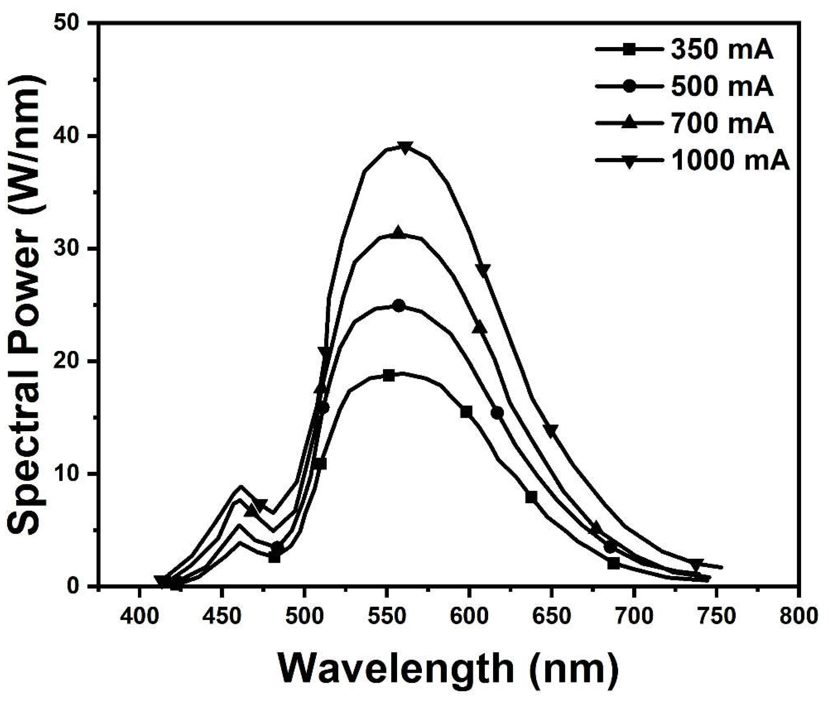
For the electroluminescence spectra experiment, we used a spectroradiometer to measure the radiation intensity of CSP-LEDs with different wavelengths and currents. To investigate the electroluminescence (EL) spectra of the fabricated FS-PiC-based white CSP-LEDs, we used a spectrometer (QE65000, Ocean Optics, USA) to measure the EL spectra. We measured the EL spectra at different driving currents, ranging from 50 mA to 1 A. Figure 10 presents the EL spectra of the FS-PiC-based white and conventional LEDs at a driving current of 1 A. The EL spectra of the FS-PiC-based white LEDs are broader than those of the traditional LEDs, indicating that the FS-PiC layer can effectively broaden the EL spectrum. Using a micro-square, the EL spectrum can be measured using a spectrometer to analyze the emitted light from an LED. We can adjust the current to drive the WLED lamp from 350 mA to 1000 mA. By examining the EL spectrum, you can identify the peak emission wavelength (PWL) of the phosphor used in the LED with micro-square via.
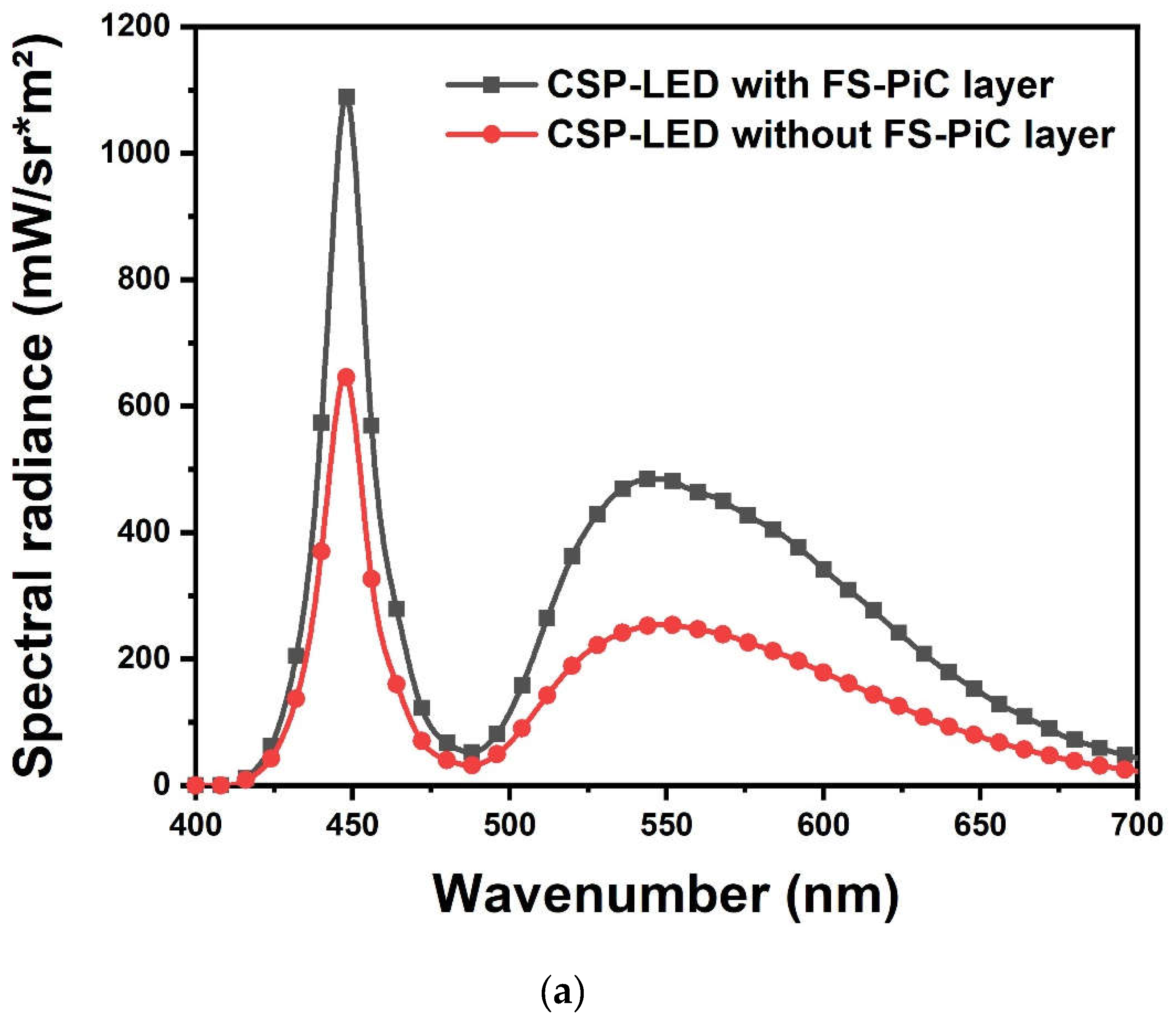
The radiation intensity of the CSP-LED is wavelength-dependent, as evidenced by the varying emission spectra. The measurement repeatability of the radiation intensity was evaluated by performing multiple measurements under the same conditions. The repeatability was calculated using the standard deviation and expressed as the mean value. The performance of CSP-LEDs depends on several factors, such as the thickness and concentration of the phosphor film on the top and side surfaces of the chip and the current density of the CSP-LEDs in Figure 11a,b. The measurement results of the micro-square via structure phosphor with blue LED showed a luminance intensity of 485 mW/srm².
In comparison, the blue LED without the structure had a measured luminance intensity of 160 mW/srm². The light intensity of the five-surface structure was higher than 2.03 times. These results indicate that the photoluminescent properties of the phosphors are significantly improved when combined with the micro-square via structure. The micro-square via structure enhances the light extraction efficiency and directs the emitted light in the desired direction. This structure allows more light from the phosphor to escape from the LED chip, increasing the luminous intensity.
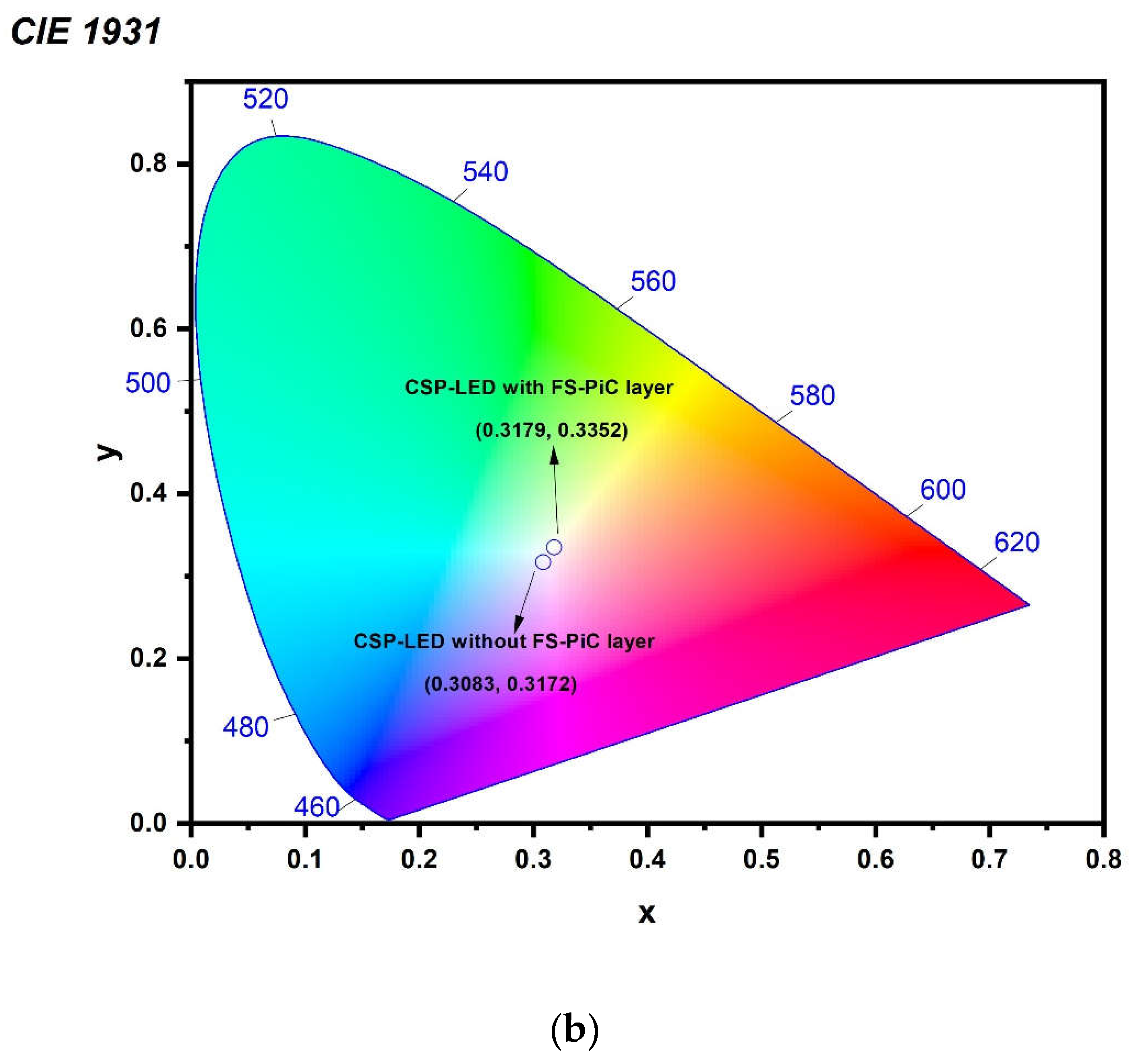
The luminous flux measures the perceived power of light emitted by a source. With the increase in thickness and concentration of the phosphor film, the luminous flux of CSP-LEDs decreases because the phosphor layer absorbs more blue light, resulting in the emission of less white light. The top surface film thickness ratio to the side surface film thickness affects the light distribution curve. However, decreasing the film thickness too much can also reduce the luminous flux due to incomplete conversion of blue light into white light. The YAG: Ce3+ phosphor with microstructure exhibited higher photoluminescence intensity under blue light excitation than the phosphor without microstructure. The main factor for this is that the microstructure enhances the light scattering and absorption of the phosphor, thereby enabling a more efficient transfer of energy from blue light to Ce3+ ions. But, the effect makes the performance of the FS-PiC LED on the color coordinate close to the white light standard in the (0.33, 0.33) when the color coordinates in five-surface structure and traditional type was of (0.3179±0.003, 0.3352±0.003), and (0.3083±0.07, 0.3172±0.07). The offset in the SS-PiC was higher than 2.6 times with the FS-PIC and was close in the blue light area.
Figure 11. The spectral luminous efficiency and CIE chromaticity coordinates of the CSP-LED without/with FS-PiC layer.
Preprints 104826 g011aPreprints 104826 g011b
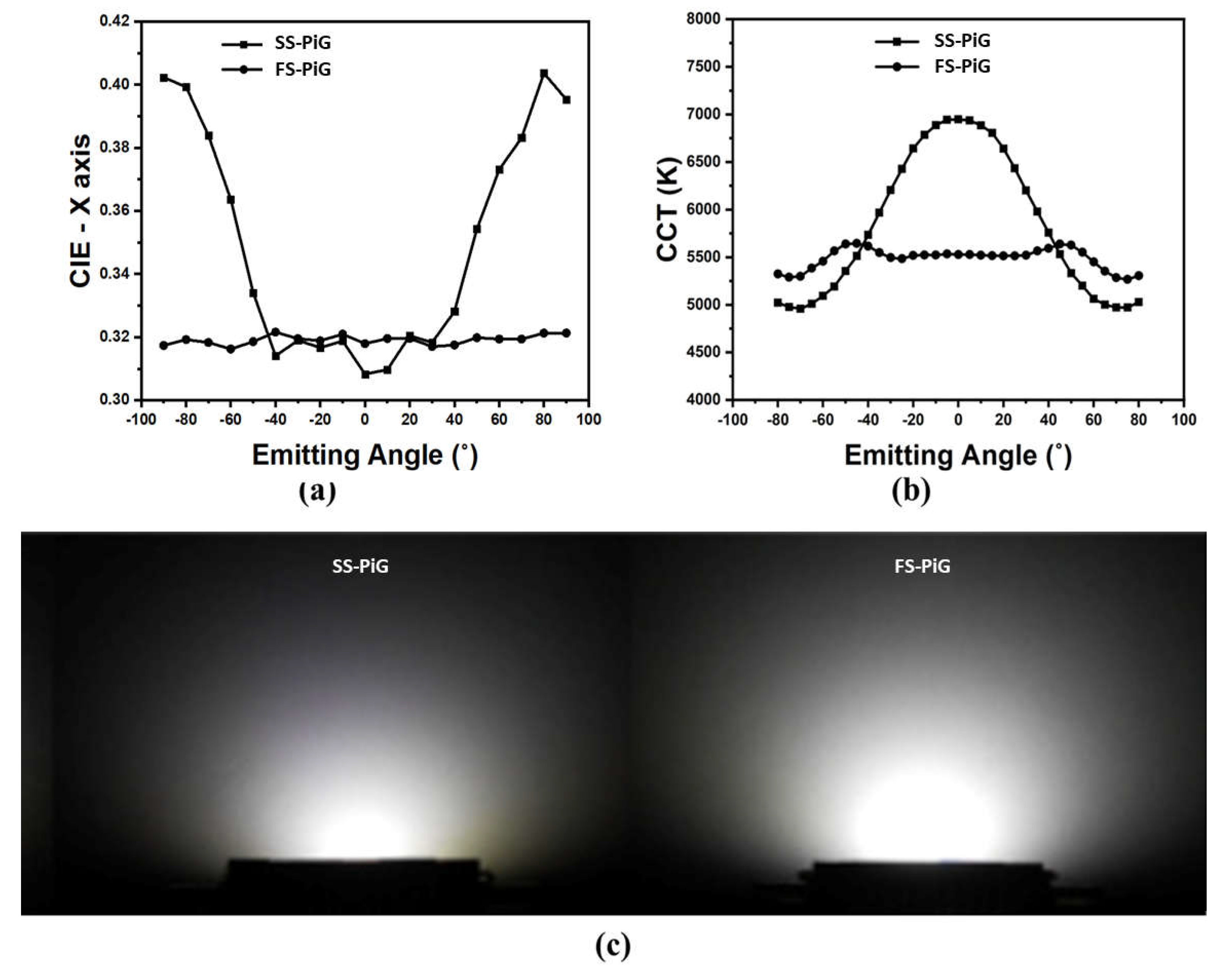
Figure 12 shows the advantages of emitting light type in the different emitting angles, which compares color coordinate distribution, CCT, and luminous performance. Figure 12(a) shows the X-axis profile analysis of IEC in the SS-PiC and FS-PiC. The center points of SS-PiC and FS-PiC were similar and close at 0.31 and 0.32, but the standard deviation gap was 23 times when the values were 0.07 and 0.003, respectively.
At the same time, the above trends are also reflected in color temperature at various emitting angles. Under color temperature measurement in Figure 12(b), SS-PiC LEDs have a color temperature range from 5000~7000 K due to their structure, with an average color temperature of 5800K. Still, the overall color temperature ranges from neutral color light (3300~5300K) to cold color light (above 5300K). The neutral color temperature area accounts for 36%, and the cold light area accounts for 64%, which is biased toward the cold light area in Figure 11(b). The average of the FS-PiG is 5500K, and the whole is at the junction of neutral and cold colors. The deviation value of FS-PiG in 110K is more uniform than the SS-PiG in 758K. Finally, the light-emitting area of FS-PiG was 3 times larger than the SS-PiG when PiG used a laser engraving process to engrave the five-surface structure and induce more light-emitting area.
The advantages of five-surface emitting white light LEDs in terms of light uniformity, softer illumination, and broader lighting effects in optical measurement and sensor applications are as follows:
  • Improved precision: Uniform light distribution can enhance measurement accuracy in optical measurements. The uniform light generated by FS-PiG LEDs helps reduce measurement deviations caused by uneven light spots or shadows.
  • Reduction of deviations: Softer light can reduce light reflection and refraction, thereby minimizing optical deviations that may occur in sensors, enhancing measurement accuracy and reliability.
  • Increased coverage: Due to the broader illumination range, FS-PiG LEDs can cover larger sensing areas, expanding the application range of sensors to accommodate a wider variety of objects of different sizes and shapes.
  • Reduced calibration requirements: Uniform and soft lighting helps reduce the calibration needs of sensors. Sensor calibration becomes more accessible and accurate with a more stable and consistent light environment for measurements.
Based on these advantages, the benefits of five-surface emitting white light LEDs in optical and sensor applications can enhance measurement accuracy, reliability, and stability, thereby enhancing sensor systems' performance and application value. Based on the literature [18], using LED instead of incandescent lights as the calibration source to calibrate the photometer for measuring LED illumination can significantly reduce the uncertainty associated with spectral mismatch correction. Switching from incandescent lamps to LED calibration sources reduces the average maximum spectral mismatch error of LED measurements by a factor of three.
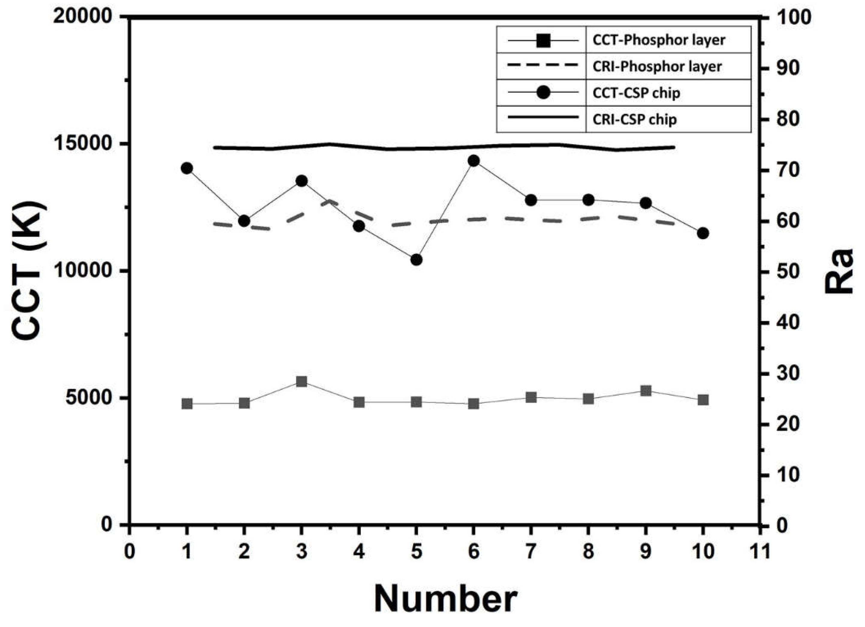
To evaluate the color performance of the fabricated FS-PiC-based white LEDs with CSP, we measured the color coordinates using a chromaticity meter (CS-200, Konica Minolta, Japan). Measured the color coordinates at different driving currents, ranging from 50 mA to 1 A. Figure 13 shows the FS-PiC-based white and conventional LEDs' chromaticity coordinates at different driving currents. The chromaticity coordinates of the FS-PiC-based white LEDs are stable at different driving currents, indicating that the FS-PiC layer has excellent color stability. Moreover, the chromaticity coordinates of the FS-PiC-based white LEDs are closer to the standard illuminant D65 than those of the conventional LEDs, indicating that the FS-PiC-based white LEDs have better color rendering.

3.3. Thermal Stability

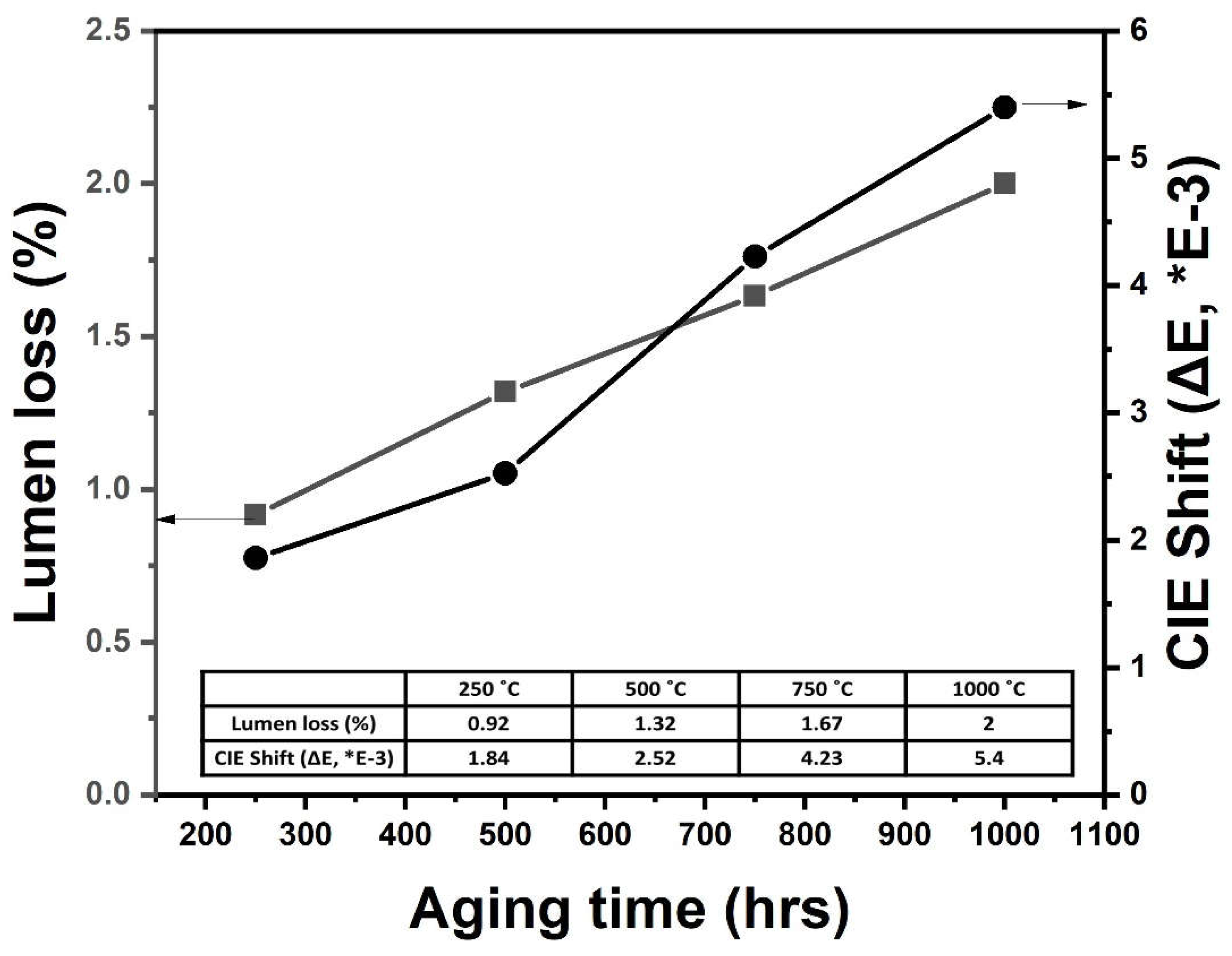
To evaluate the thermal stability of the fabricated FS-PiC-based white CSP-LEDs, we conducted accelerated aging tests at a temperature of 350°C for 1008 hours. We evaluated the thermal stability by measuring the optical output power and color coordinates before and after the accelerated aging tests. We observed that the measured optical output power and color coordinates of the FS-PiC-based white LEDs and conventional LEDs before and after accelerated aging tests did not change the content. The FS-PiC-based white LEDs exhibited lumen loss of only 2% and less chromaticity shift of 5.4x10⁻³, which were much lower than those of conventional LEDs. The high ceramic melting temperature of up to 510°C contributes to the good thermal stability of the FS-PiC. To evaluate the thermal performance of the FS-PiC-based white LEDs, we performed accelerated aging tests on the LEDs by placing them in an oven at 350°C for 1008 hours. We monitored the LEDs' lumen maintenance and chromaticity shift during the aging process. After 1008 hours of aging at 350°C, the lumen maintenance of FS-PiC-based white LEDs exceeds 98%, demonstrating remarkable thermal stability. The chromaticity shift during the aging process is minimal, with the LEDs' coordinates shifting slightly from (0.32, 0.33) to (0.33, 0.34), corresponding to a chromaticity shift of 5.4x10⁻³. The high ceramic melting temperature of up to 510°C contributes to the good thermal stability and low chromaticity shift of FS-PiC-based white LEDs, preventing the phosphor from decomposing and diffusing into the epoxy resin under high-temperature conditions. The aging test process is shown in the Fugure 14.

4. Discussion and Conclusions

In summary, we have demonstrated a novel FS-PiC structure for chip scale package white LEDs, which exhibits excellent optical performance and high reliability. We performed the laser engraving process on the surface of an FS-PiC layer. The laser engraving resulted in a well-defined and controlled surface morphology on the phosphor layer, creating intricate patterns and structures within the phosphor layer. This deep laser engraving capability opens up possibilities for various applications that require precise and profound modifications within the PiC layer. The saddle-shaped FS-PiC structure can achieve high color uniformity with controllable top and side thicknesses, and the yellow phosphor in ceramic composite has a high ceramic melting temperature of up to 510°C, which provides excellent thermal stability for the LEDs.
The performance of the FS-PiC LED exhibited the illumination of 401lm, average color temperature (CCT) of 5488K±110K, and color coordinates (CIE) of (0.3179±0.003, 0.3352±0.003). In contrast to the single-surface phosphor-in-ceramic (SS-PiC), it exhibited the illumination of 380lm, average CCT of 5830K±758K, and CIE of (0.3083±0.07, 0.3172±0.07). These indicated that the performance of the FS-PiC was higher than the illumination, CCT, and CIE of 1.1, 7, and 23 times, respectively, for the SS-PiC. The FS-PiC-based white LEDs exhibit lumen loss of only 2% and less chromaticity shift of 5.4x10⁻³ chromaticity shift after 1008 hours of aging at 350°C, indicating excellent thermal stability and reliability. The proposed FS-PiC-based white LEDs with CSP benefit as promising candidates to replace the current phosphor-in-organic silicone in high-power LEDs for the next generation of illumination, display, and headlight applications.

5. Funding and Disclosures

5.1. Funding

Ministry of Science and Technology, Taiwan (MOST) National Science and Technology Council (111-2221-E-005-023-MY3, 111-2221-E-005-024-MY2, 111RB02); Ministry of Education (110RA077A, 111RA077A).

5.2. Disclosures

The authors declare no conflicts of interest.

References

  1. Pust, P.; Schmidt, P. J. and Schnick, W. A revolution in lighting. Nat. Mater. 2015, 14, 454–458. [Google Scholar] [PubMed]
  2. McKittrick, J.; Shea-Rohwer, L. E. Review: Down conversion materials for solid-state lighting. J. Amer. Ceram. Soc. 2014, 97, 1327–1352. [Google Scholar] [CrossRef]
  3. Chen, K. J.; Han, H. V.; Chen, H. C.; Lin, C. C.; Chien, S. H.; Huang, C. C.; Chen, T. M.; Shih, M. H.; Kuo, H. C. White light-emitting diodes with enhanced CCT uniformity and luminous flux using ZrO2 nanoparticles. Nanoscale 2014, 6, 5378–5383. [Google Scholar] [CrossRef] [PubMed]
  4. Ding, X.; Li, J.; Chen, Q.; Tang, Y.; Li, Z.; Yu, B. Improving LED CCT uniformity using micropatterned films optimized by combining ray tracing and FDTD methods. Opt. Exp. 2015, 23, A180–A191. [Google Scholar] [CrossRef] [PubMed]
  5. Liu, Z. Y.; Li, C.; Yu, B. H.; Wang, Y. H.; Niu, H. B. Effects of YAG: Ce phosphor particle size on luminous flux and angular color uniformity of phosphor-converted white LEDs. J. Display Technol. 2012, 8, 329–335. [Google Scholar] [CrossRef]
  6. Sommer, C.; Krenn, J. R.; Hartmann, P.; Pachler, P.; Schweighart, M.; Tasch, S.; Wenzl, F. P. The effect of the phosphor particle sizes on the angular homogeneity of phosphor-converted high-power white LED light sources,” IEEE J. Sel. Top. Quant. 2009, 15, 1181–1188. [Google Scholar] [CrossRef]
  7. Li, J. S.; Chen, Y. H.; Li, Z. T.; Yu, S. D.; Tang, Y.; Ding, X. R.; Yuan, W. ACU optimization of pcLEDs by combining the pulsed spray and feedback method. J. Display Technol. 2016, 12, 1229–1234. [Google Scholar] [CrossRef]
  8. Li, J.; Li, Z.; Liang, G.; Yu, S.; Tang, Y.; Ding, X. Color uniformity enhancement for COBWLEDs using a remote phosphor film with two freeform surfaces. Opt. Exp. 2016, 24, 23685–23696. [Google Scholar] [CrossRef] [PubMed]
  9. Liu, Z.; Liu, S.; Wang, K.; Luo, X. Optical analysis of color distribution in white LEDs with various packaging methods. IEEE Photon. Technol. Lett. 2008, 20, 2027–2029. [Google Scholar]
  10. Kuo, H. C.; Hung, C. W.; Chen, H. C.; Chen, K. j.; Wang, C. H.; Sher, C. W.; Yeh, C. C.; Lin, C. C.; Cheng, Y. J. Patterned structure of remote phosphor for phosphor- converted white LEDs. Opt. Exp. 2011, 19, A930–A936. [Google Scholar] [CrossRef] [PubMed]
  11. Zheng, H.; Zhao, Z.; Wang, Y.; Li, L.; Liu, S. Effect of patterned substrate on light extraction efficiency of chip-on-board packaging LEDs, in IEEE 64th Electron. Compon. Technol. Conf. (ECTC) 2014, 1876–1879. [Google Scholar]
  12. Mao, P.; Mahapatra, A. K.; Chen, J.; Chen, M.; Wanf, G.; Han, M. Fabrication of Polystyrene/ZnO Micronano Hierarchical Structure Applied for Light Extraction of Light-Emitting Devices. ACS Appl. Mater. Interfaces 2015, 7, 19179–19188. [Google Scholar] [CrossRef] [PubMed]
  13. Sun, B.; Zhao, L.; Wei, T.; Yi, X.; Liu, Z.; Wang, G.; Li, J.; Yi, F. Light extraction enhancement of bulk GaN light-emitting diode with hemisphere-cones-hybrid surface. J. Display Technol. 2013, 9, 317–323. [Google Scholar] [CrossRef] [PubMed]
  14. Li, Z.; Tang, Y.; Li, J.; Wu, C.; Ding, X.; Yu, B. High Color Uniformity of White Light-Emitting Diodes Using Chip-Scaled Package. IEEE Photonic. Tech. L. 2018, 30, 989–992. [Google Scholar] [CrossRef]
  15. Li, Z. T.; Tang, Y.; Liu, Z. Y.; Tan, Y. E.; Zhu, B. M. Detailed study on pulse-sprayed conformal phosphor configurations for LEDs. J. Display Technol. 2013, 9, 433–440. [Google Scholar] [CrossRef]
  16. Zheng, H.; Ma, J.; Luo, X. Conformal phosphor distribution for white lighting emitting diode packaging by conventional dispensing coating method with structure control. IEEE Trans. Compon. Packag. Manuf. Technol. 2013, 3, 417–421. [Google Scholar] [CrossRef]
  17. Kwon, S. B.; Yoo, J. H.; Choi, S. H.; Na, M.; Kim, B. Y.; Lee, S. Y.; Jeong, H. J.; Kim, W. H.; Park, S. H.; Yoon, H. S.; Kang, B. K.; Song, Y. H.; Yoon, D. H. Preparation of high-quality YAG:Ce3+ ceramic phosphor by high-frequency induction heated press sintering methods. Sci. Rep. 2022, 12, 20477. [Google Scholar] [CrossRef]
  18. Pulli, T.; Dönsberg, T.; Poikonen, T.; Manoocheri, F.; Kärhä, P.; Ikonen, E. Advantages of white LED lamps and new detector technology in photometry. Light Sci. Appl. 2015, 4, e332. [Google Scholar] [CrossRef]
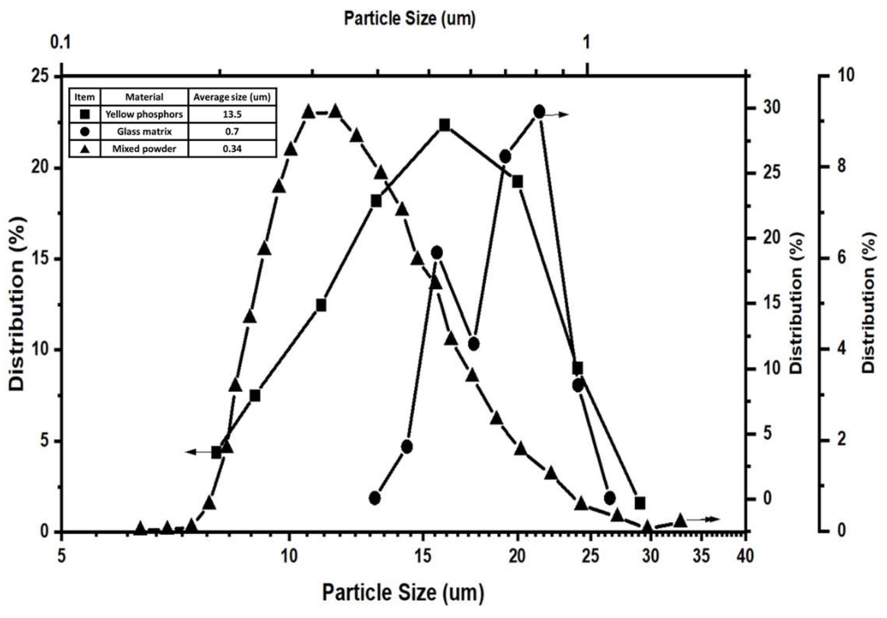
Figure 1. The measurement of single/mixed powder distribution. ■ is the yellow phosphors powder, and the average size is 13.5um; ● is the glass matrix powder, and the average size is 0.7um; ▲ is the mixed powder mixer for 4 hours at 450 rpm, and the average size is 0.34um.
Preprints 104826 g001
Figure 2. Schematic diagram of PiC wafer cutting and grinding process.
Preprints 104826 g002
Figure 4. (a) PiC wafer, (b) FS-PiC wafer, (c) FS-PiC structure.
Preprints 104826 g004
Figure 5. FS-PiC of CSP-LED array board and LED chip size.
Preprints 104826 g005
Figure 6. A test sample of CSP-LED.
Preprints 104826 g006
Figure 7. Optical image analysis of PiC: (a) top view in the 2D image, (b) tilt angle in the 3D image, and (c) sectional view in the 3D image.
Preprints 104826 g007
Figure 8. Optical image analysis of FS-PiC: (a) top view in the 2D image, (b) tilt angle in the 3D image, and (c) sectional view in the 3D image.
Preprints 104826 g008
Figure 9. Luminous flux power of the CSP-LED.
Preprints 104826 g009
Figure 10. Spectral luminous efficiency of the CSP-LED.
Preprints 104826 g010
Figure 12. The optical measurement in the (a) X-axis profile distribution in the CIE, (b)CCT, and (c) emitting area of the FS-PiG and the SS-PiG.
Preprints 104826 g012
Figure 13. The spectral power distribution.
Preprints 104826 g013
Figure 14. The test result of lumen loss and CIE shift when FS-PiC is 350 ˚C and passes to 10008 hrs.
Preprints 104826 g014
Table 1. The fabrication parameter for the PiC wafer.
Glass matrix (wt%) YAG: Ce3+ (wt%) Sintering temperature (˚C) Diameter (in)
PiC 84 16 700 4
Table 2. Picosecond laser parameters.
Parameter
Wavelength 1064 nm
Laser power 44 W
Pulse repetition rate 350 kHz
Focal spot diameter 13μm to 15 μm
Pulse width 15 ps
Cutting speed 1300 mm/s
Disclaimer/Publisher’s Note: The statements, opinions and data contained in all publications are solely those of the individual author(s) and contributor(s) and not of MDPI and/or the editor(s). MDPI and/or the editor(s) disclaim responsibility for any injury to people or property resulting from any ideas, methods, instructions or products referred to in the content.
Copyright: This open access article is published under a Creative Commons CC BY 4.0 license, which permit the free download, distribution, and reuse, provided that the author and preprint are cited in any reuse.
Prerpints.org logo

Preprints.org is a free preprint server supported by MDPI in Basel, Switzerland.

Subscribe

© 2024 MDPI (Basel, Switzerland) unless otherwise stated