1. Introduction
Edge computing is the provision of services for end applications that would require a server on the Internet but should reach it with low latency. The closer the edge computer gets to the user (so-called far edge computing), the more specific the requirements for the edge service become. A very specific application here is, for example, Deep Learning (DL) [
2]. DL is a promising area for the use of computing services in the cloud and at the edge. But DL also requires pre- and post-processing of data. To first test the special properties of our co-processors using a simpler example, we decided to develop an FFT accelerator. The relevance of this can be seen in E. L. Chuma and Y. Iano. Their research focuses on human motion detection. To do this, they use the FFT as a preprocessing stage for a neural network in a corresponding IoT application [
3] (IoT: Internet of Things).
So, if an IoT end device needs more computing power than it can provide itself, but cannot tolerate the usual delays to the server, edge computing is an option. The edge computer then makes its computing capacity available to IoT-devices like mobile systems. Signal processing applications would benefit from the presence of a dedicated digital signal processor (DSP) or field programmable gate array (FPGA) on board a mobile device. However, this is not possible for small or low-energy IoT devices and so they could alternatively use the services of an edge computer. Instead, we would like to see the special computing units listed above on the edge computer side. Consequently, an edge computer should contain DSPs or FPGAs as computing accelerators. Here we suggest relying entirely on FPGAs, as DSPs are far too specialized. FPGAs, on the other hand, contain large numbers of DSP-typical computing units and can replace DSPs and surpass them in terms of computing power. In addition, FPGAs can be used more universally and are not limited to accelerating signal processing algorithms.
The "FPGA on the Edge" project was a publicly funded feasibility study in which we developed a co-processor to accelerate the FFT algorithm [
4]
1. We initially targeted mobile systems in various areas of application, such as drones for logistics or surveillance tasks. For example, autonomous flight control requires the processing of sensor data in hard real time. Excessive dead times could lead to an unstable controller. The design of an on-board computer for small drones must meet very strict requirements in terms of volume, weight, and energy requirements, because as many of the available resources as possible should be reserved primarily to the operational components (e.g. sensors). Using the computing capacity of an edge computer therefore makes sense and increases flight safety if low latency can be guaranteed.
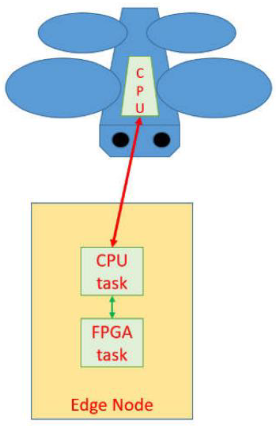
Figure 1 shows a drone that we assume has very limited CPU capacity. The communication link to an edge node is shown. The compute node in
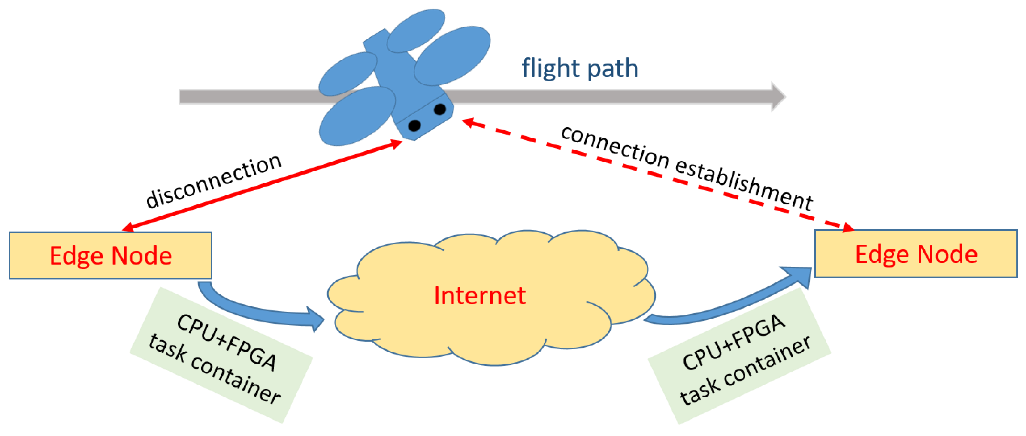
Figure 1 provides a powerful CPU equipped with an FPGA-based co-processing environment that supports the drone. Another point in our feasibility study was to consider mobile scenarios in which the end device moves between different access points of an edge computing provider. This happens with drones that, for example, accompany ships in coastal pilotage and fly through several cell phone cells. Similar applications would be monitoring traffic routes or inspecting pipelines or electrical supply lines. To do this, there would then have to be similar edge nodes in every radio cell flown through. This type of mobility (see
Figure 2) is then supported by a so-called handover mechanism between edge nodes. In our case, the handover not only includes setting up the software but also requires reconfiguration of the co-processor.
Basically, when handing over between two edge nodes, the current state of the co-processor must be packed into a so-called container. This container is then transported to the target node via the Internet (or an intranet). In the target node, the original situation of the source node is then reconstructed. This also includes the corresponding HW accelerator including its last calculation state. (Note: The project was worked on during the pandemic situation and was subject to certain restrictions. Therefore, only a subset of the planned work could be realized. The handover mechanism therefore remained open.)
To be able to implement this type of handover mechanism, reasonable handling of the container concept must be considered when developing co-processors. A complete transmission of the FPGA configuration, the so-called bit stream, does not make sense. Instead, the target node, as every node in the system, holds a library of compatible co-processors in its main memory for reconfiguration. It must therefore be ensured that the state of the co-processor can be read and reconstructed. Then it only becomes necessary to load the transmitted status into the compatible co-processor.
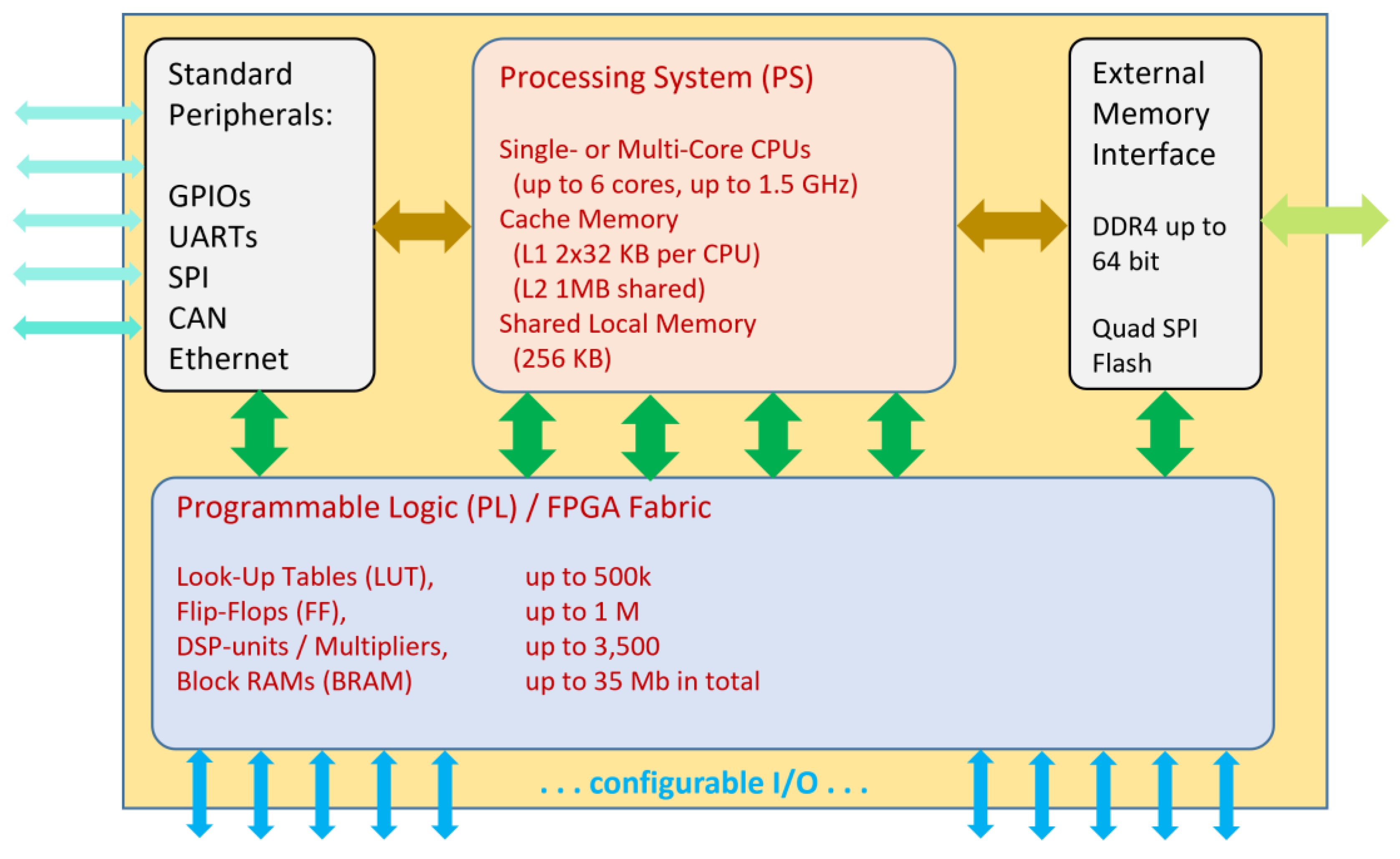
The FPGA technology that we propose to edge nodes is based on a so-called System on Programmable Chip (SoPC). These are platforms that combine a processor system (PS) and programmable logic (PL) on a microchip. The combination of PS and PL in one chip results in a tight coupling between these two areas, providing high data bandwidth and low latency. These properties make the PL part ideal for implementing HW accelerators in real-time applications. Since the PL part is ultimately an FPGA, you get a domain of configurable co-processors, so to speak. A suitable FPGA design flow is required for developments in the PL part of the SoPC.
Figure 3 shows a typical SoPC. The numbers do not correspond to any specific device but rather, the numbers provide an idea of the possibilities. At the center is the PS, which can represent a complete computer with the help of external RAM and external peripheral interfaces. Of the standard peripherals, the edge node essentially still requires the Ethernet connection. The interesting aspect of a SoPC is the PL part, sometimes called the “FPGA” fabric. The configurable hardware mainly provides the following resources:
Look-Up Tables (LUT),
Flip-Flops (FF),
DSP units and
Block RAMs (BRAM).
LUTs and FFs are the physically smaller and more numerous components. Typically, a multitude of LUTs and FFs are contained within larger resources called Configurable Logic Blocks (CLBs), which often also host other small circuits such as multiplexers. LUTs implement the combinational part of a logic circuit and FFs represent the memorizing elements for sequential circuits. DSP units contain at least hardware multipliers. Sometimes they are also complete Multiply-Accumulate units (MAC). For BRAMs, only the total amount of memory is shown in
Figure 3. The number given for BRAM here represents the total sum of memory bits. Many smaller memory blocks contribute to this number. All BRAMs can be used independently of one another, which is particularly important for parallel signal processing. The configurable I/Os shown in the Figure play either no role or only a minor one for HW accelerators. The SoPC, equipped with external memory and standard peripherals, can directly implement an edge node. It is also conceivable to use it as a plug-in card for a standard server.
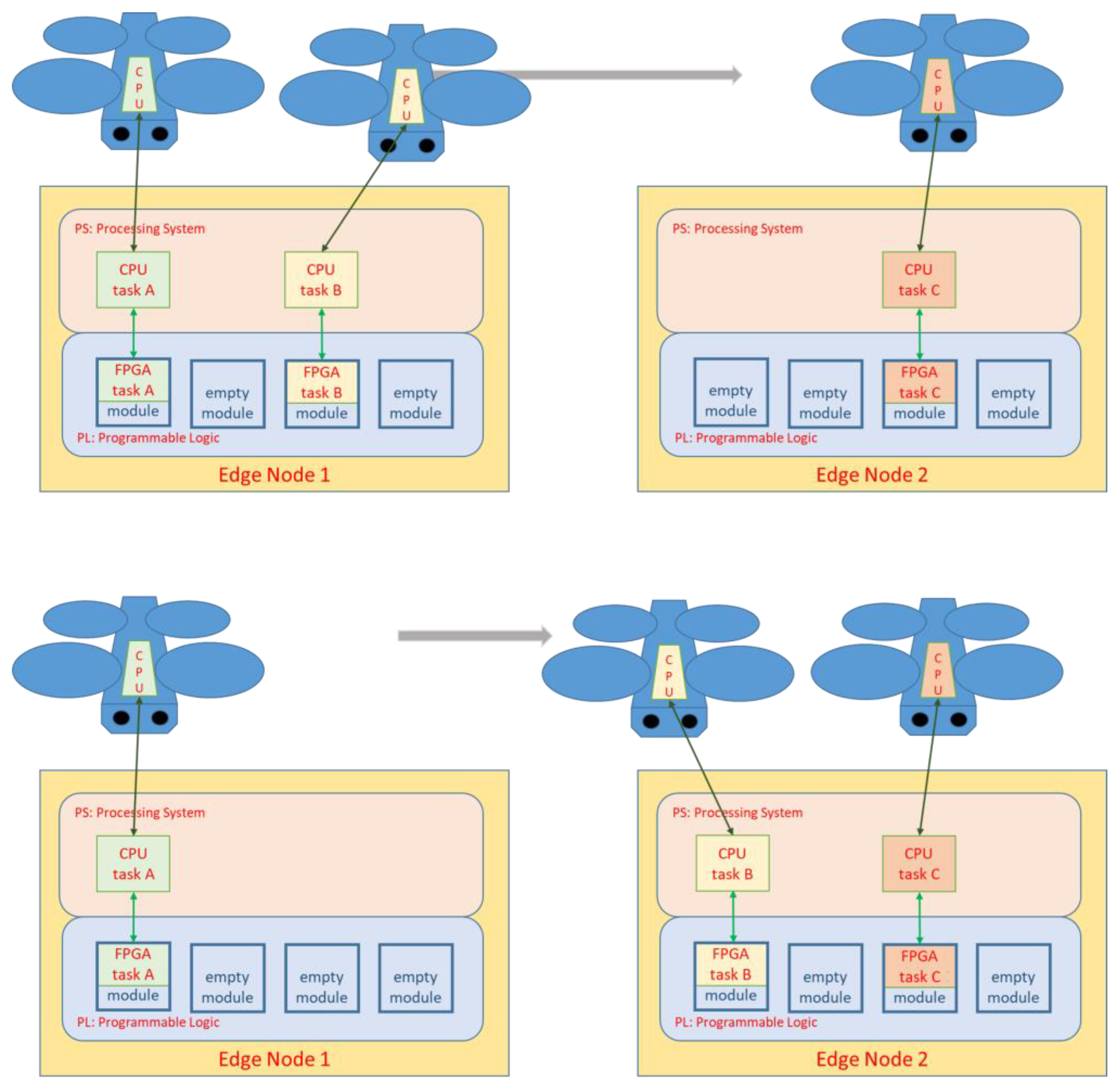
As part of the feasibility study, we initially limit ourselves to the implementation of an FFT accelerator unit. This is part of a co-processor that resides in the PL part of the edge node as a replaceable configuration. Multiple mobile devices (e.g. drones) should be able to use PL-implemented services of an edge computing node at the same time. How many co-processors of which complexity can be used is a question of the amount of available PL resources and therefore also a question of costs. Thus, an SoPC-based edge computer can provide a limited number of co-processors operating concurrently. Different mobile clients with possibly different computing needs may require different co-processors, which should be able to be configured independently of one another. These configuration scenarios are subject to constant changes due to the dynamics of multiple mobile clients. However, in order to be able to operate different co-processors independently at the same time in dynamic configuration scenarios, the use of the “partial reconfiguration” method is absolutely necessary.
Figure 4 is intended to explain these circumstances. There we have three drones and two edge computing nodes in two different radio cells (radio cells not shown). The three drones are currently having different tasks processed: tasks A, B and C. Each task consists of a software component that is processed in the PS on different CPU cores or in multitasking, and a HW accelerator, called an FPGA task. The execution of an FPGA task takes place in a module which occupies one slot. The module slots are prepared and are either empty or contain the requested co-processor. As a first approach the PL layout with the module slots is identical on all edge nodes. However, as you can see in the picture, when changing the node, the FPGA task B cannot be executed on the same module space because this is already occupied by FPGA task C. So, we have a requirement here that a specific co-processor must be executable on different module slots.
The FPGA-based edge computing approach we describe with special consideration of mobile systems is new and combines concepts from different domains, which are discussed in the following subsections.
1.1. Edge Computing for Mobile Systems
Research work has already been carried out to support mobile systems using edge computing. Y. Cao and Y. Chen conducted research in the field of “Internet for Vehicles”. For example, they developed a Quality of Experience (QoE) node selection (QNS) strategy to reduce the network bandwidth bottleneck [
5]. For the uninterrupted operation of mobile clients, L. Ma et. Al. worked on a service handoff system. A key aspect was the low end-to-end latency [
6].
1.2. FPGA-based Co-Processing
The purpose of early FPGAs in computer systems was primarily to replace so-called "glue logic", but this has since expanded to include use in co-processing. Tom Hill describes in particular the advantages of FPGA co-processing for digital signal processing in his Xilinx white paper [
7]. Partial reconfiguration is also a topic that the FPGA manufacturer Xilinx highlights in its documentation. C. Kohn has written an application note [
8], which is particularly concerned with hardware accelerators based on the so-called Zynq components. Especially for hardware tasks in edge computing, Z. Zhu et. Al. propose their “Dynamic Partial Reconfiguration” (DPR) approach [
9]. The method includes a task scheduling framework for these hardware tasks. The authors describe the basic principles of the partial reconfiguration procedure and supplement this with some case studies.
There are two interesting recent publications. The first comes from the research group behind the acronym VEDLIoT. VEDLIoT is, among other things, concerned with FPGA-based hardware acceleration of certain DL algorithms [
2]. The partial and dynamic reconfiguration should make it possible to choose between different DL accelerators at runtime. Another article by M. Monopoli et al. describes a so-called “soft” graphics processing unit (GPU) that can be used on a SoPC platform [
10]. Dynamic partial reconfiguration is part of the concept.
1.3. FPGA-based FFT-Acceleration
The FFT is one of the most fundamental algorithms in the field of digital signal processing. As a numerically complex core algorithm, diverse and highly efficient variants of the FFT have been developed in the past. The implementations were initially carried out for signal processors and general-purpose architectures. Almost as long as FPGAs have existed, they have been included in considerations of efficient FFT execution, as we can see in [
11,
12,
13,
18,
19,
20,
21]. The so-called “butterfly” architecture forms the basis for both the software implementation and the hardware acceleration. There are, among others, the Radix-2 or Radix-4 based FFT algorithms [
12]. A butterfly as a computing core is executed or used several times depending on the size of the time series to be transformed. Apart from [
13], most of the FPGA-based FFT implementations considered here are based on the use of memory blocks. Therefore, it is obvious to use internal RAM blocks (BRAMs) for FPGA implementations [
14].
2. Materials and Methods
This chapter is divided into three sections of different sizes. After a very short section about prototype hardware, the main part follows with the description of the actual co-processor development. The final section then describes the reconfiguration properties of our approach.
2.1. Edge Node Prototype Hardware
The core component is a so-called Zynq Ultrascale+ MPSoC (multi-processor system-on-chip) from the manufacturer Xilinx (now AMD). Ultrascale+ MPSoC is a manufacturer-specific term [
14] for the corresponding microchip. It is a component from the SoPC category described above.
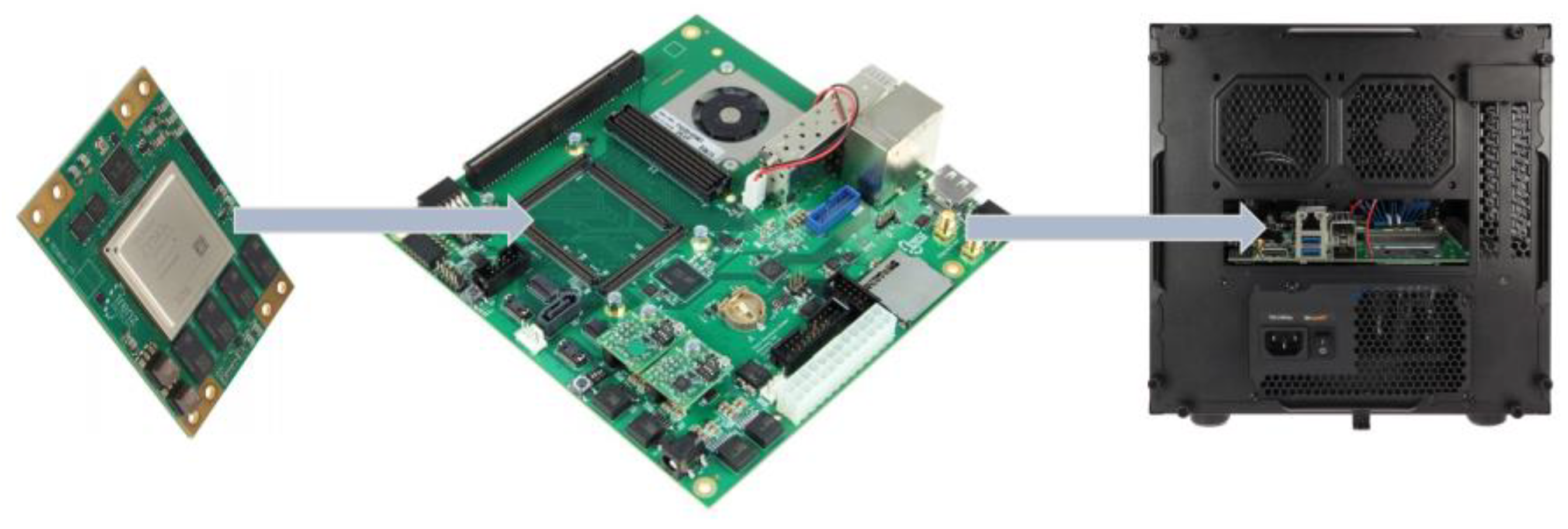
The project was developed using a so-called “starter kit” from Trenz [
15]. It consists of an UltraScale+ MPSoC module which is located on a suitable base board in ITX format. All components find their place in an ITX housing as shown in
Figure 5. From the outside, the node appears like a standard mini-PC.
2.2. FFT Co-Processor Development
With a focus on partial reconfiguration and the support of a handover mechanism, we have developed an example FFT co-processor. Since these two principles represented the more important object of investigation, absolute computing power was only a secondary criterion. The hardware description language VHDL was used to develop the co-processor. The co-processor was then implemented and tested on the MPSoC module mentioned above [
16].
This chapter on the development of the FFT co-processor is divided into two subsections. The first subsection represents the main part in which we go into detail about the actual FFT accelerator unit. The second subsection then describes how the FFT accelerator unit is “packaged” into a co-processor framework.
2.2.1. FFT Accelerator Unit
We follow the approach of a "memory-based" FFT implementation. As mentioned above, it is a widely used approach for FFT-FPGA implementations. Since one has to manage with the existing BRAM blocks, there is a limit to the number of simultaneous memory reads and writes. A BRAM can be configured with two separate connection groups, allowing use as a dual-port RAM. So, you have two storage processes available in one machine cycle. Of course, the greatest possible parallelism should be sought for a hardware accelerator. To do this, we combine the memory-based FFT implementation approach with the multi-port memory design described in [
17]. Assuming a similar clock frequency in the implementation of such a design and a typical pure BRAM design, the former would involve a performance boost proportional to the gain in number of simultaneous memory read/write operations.
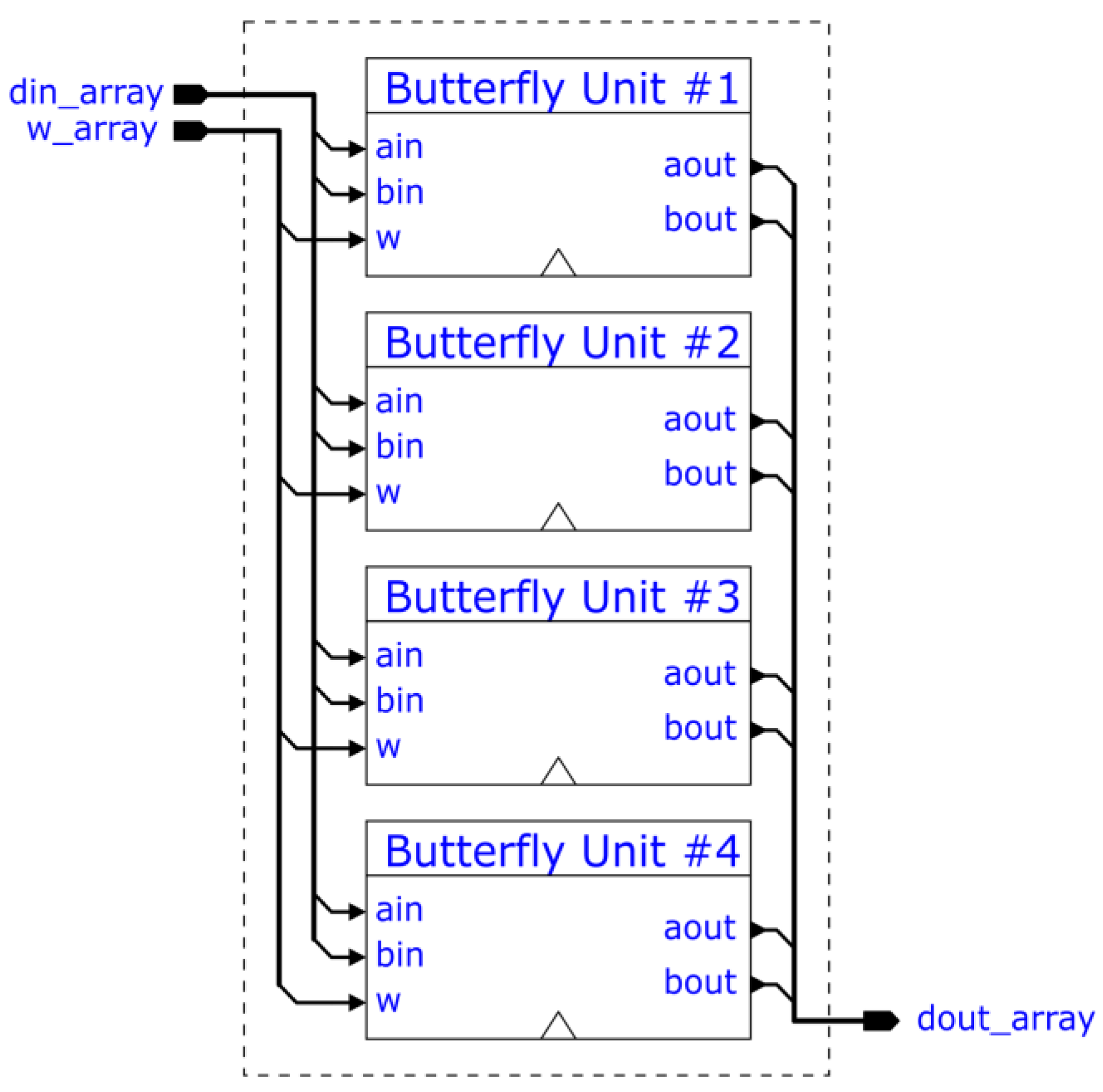
The designed FFT module supports 1024 complex data points with 32-bit real and imaginary parts in 1.31 signed fixed-point format. To make optimal use of the PL's DSP slices, the internal accuracy is however limited to 1.25 signed fixed-point format and the twiddle factors are stored in 1.16 signed fixed-point format. The core numerical operation of the FFT algorithm is the so-called “butterfly unit”, in our case more specifically the radix-2 variant. It was decided that 4 such butterfly units should work in parallel.
The implemented FFT unit is shown in
Figure 6. The input data is loaded onto the FFT RAM using the data array signal
din_array, the address array signal
addr_array, and the write enable array signal
wen_array. The
wen_array elements determine whether the respective
din_array element should be written onto the FFT RAM at the respective
addr_array address. In order to arrange the input data so that the butterfly units can perform their calculations “in place” with respect to memory, i.e. the resulting outputs overwrite the inputs in RAM, the incoming write addresses are bit-reversed. An assertion of the start signal begins the FFT calculation, in the meantime blocking external access to the RAM. The ready output signal is driven low to indicate the unit is busy. The Address Generator proceeds to calculate the addresses of data points and twiddle factors, passing them on to the Multi-ported RAM and Twiddle Factor ROM respectively. The butterfly units contained by the Butterfly Unit Bank (a diagram of which is shown in
Figure 7) perform butterfly operations with the RAM and ROM data, and pass the results back to RAM, which writes in accordance with the write enable signals received from the Address Generator. The Address Generator's
write enable and
write addresses are delayed in order to reach the RAM only when the butterfly operations pipeline is finished processing the data read from the same addresses.
The way the Address Generator calculates the two butterfly wing addresses, and the address/power of the relevant twiddle factor is well-described in [
11]. To summarize, for
N representing the number of FFT data points (in our case 1024), let:
“Butterflies/level” stands for the total amount of butterfly operations required to complete a level, hence equal to
N/2 = 1024/2 = 512. With
l and
i being counted and “//” denoting integer division, then:
Both the address generation as well as butterfly operations are fully pipelined. The address generation pipeline is 3 stages long, whilst the butterfly pipeline is 8 stages long. When all calculations are finished, the done signal is pulsed, and the ready signal is asserted. The RAM is once again made accessible externally and now contains the FFT computation results. The FFT is accessed by reading the RAM contents using the addr_array address input signal and dout_array data output signal.
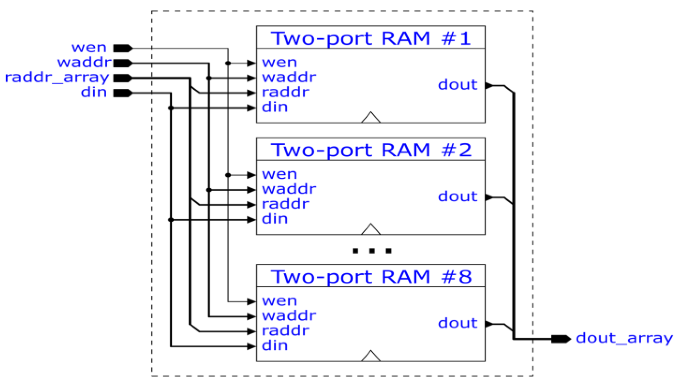
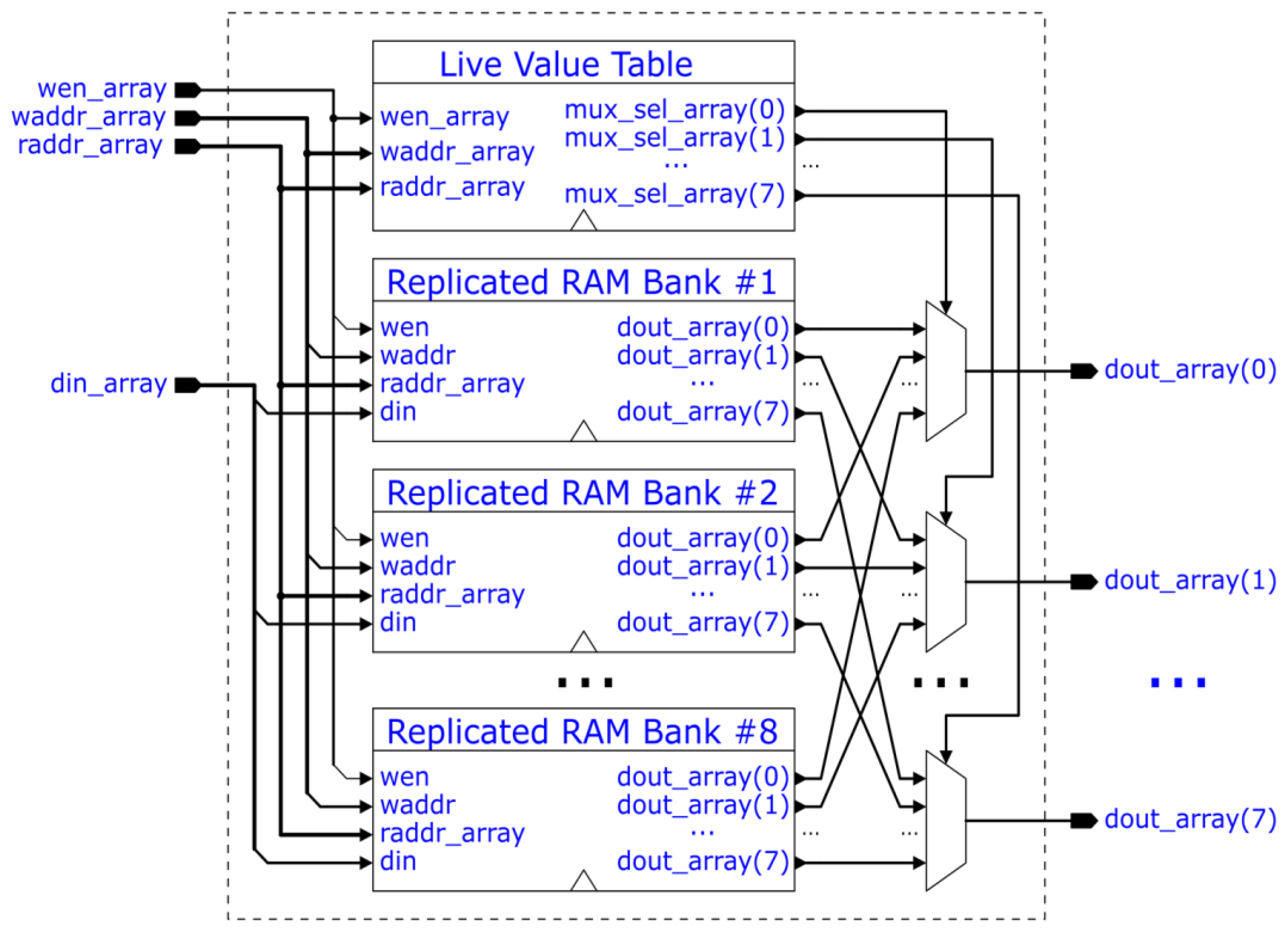
To perform four parallel butterfly operations, the RAM unit must support eight reads and eight writes per clock cycle. Such a multi-ported RAM was implemented as described in [
17] and is made up of a so-called "live-value-table" (LVT) and a series of replicated RAM banks, as shown in
Figure 8. The LVT stores an ID of a replicated RAM bank for each possible RAM address. These IDs tell which replicated RAM bank hosts the valid (most recently written) data for the respective RAM address and are used as multiplexer selectors. The LVT is essentially a multi-ported RAM itself but built out of FPGA CLBs. The structure of the replicated RAM banks is shown in
Figure 9. The design concept involves replicating two-ported (dual-ported) RAMs to gain extra read ports. In our case, 8 two-ported RAMs result in 8 read ports. Only one write port is present, which writes to all the replicated two-ported RAMs, and therefore all two-ported RAMs are up-to-date and can be safely read from.
For an edge computing node to perform a handover of its state to another node, the FFT unit must itself be able to manage state saving and loading. The ssave signal triggers the saving of the state, to which then the sresp signal informs if state saving was successful and how the saved state sout and RAM data should be interpreted. To load a state, the input state must be written to the sin input and the sload signal must be pulsed instead of start. In the case that a save request is made in the middle of an FFT calculation, the RAM contents then represent intermediary results. By the same token, the saved state sout represents the progress of the current calculation so as to allow the state-receiving edge node to properly resume the calculation.
The state of the FFT unit is two-fold: the state of the Address Generator, and the RAM contents. To fully describe the state of the Address Generator, it is sufficient to know two values: the butterfly level, and the number of the butterfly operation in the level performed by the first unit in the butterfly bank (denoted in (1) as l and i, where only the i of the first unit in the butterfly stack is relevant). The two values can fit in a total of 13 bits – 4 for the level, 9 for the butterfly operation number. These two values, concatenated, are what make up the sin and sout signals. Depending on the timing of the state save request, the sout signal as well as the RAM contents might or might not be relevant. To discern between different scenarios, the sresp signal comes in handy, able to take a different value (arbitrarily chosen) for each scenario:
“00” – default, a state save was not requested.
“01” – valid sout, unmodified FFT RAM data (due to a premature state save, i.e. no address generation had yet taken place; sout is all zeroes)
“10” – invalid sout, final FFT RAM data (due to overdue state save, i.e. address generation had finished)
“11” – valid sout, modified FFT RAM data (state save happened during FFT address generation)
A state graph of the Address Generator FSM is shown in
Figure 10, where some save request timings and related state changes are also visible. After all the addresses are generated, the wait state ensures the pipeline of butterfly operations and RAM writes is finished before pulsing the done output and entering an idle state where external RAM access is granted.
2.2.2. FFT Co-Processor
The designed FFT unit does not constitute a complete co-processor in of itself. As the FFT unit is implemented on the PL, a connection to the MPSoC's processing system (PS) must be established to facilitate communication with the software. For this purpose, we make use of the on-chip AXI bus connectors [
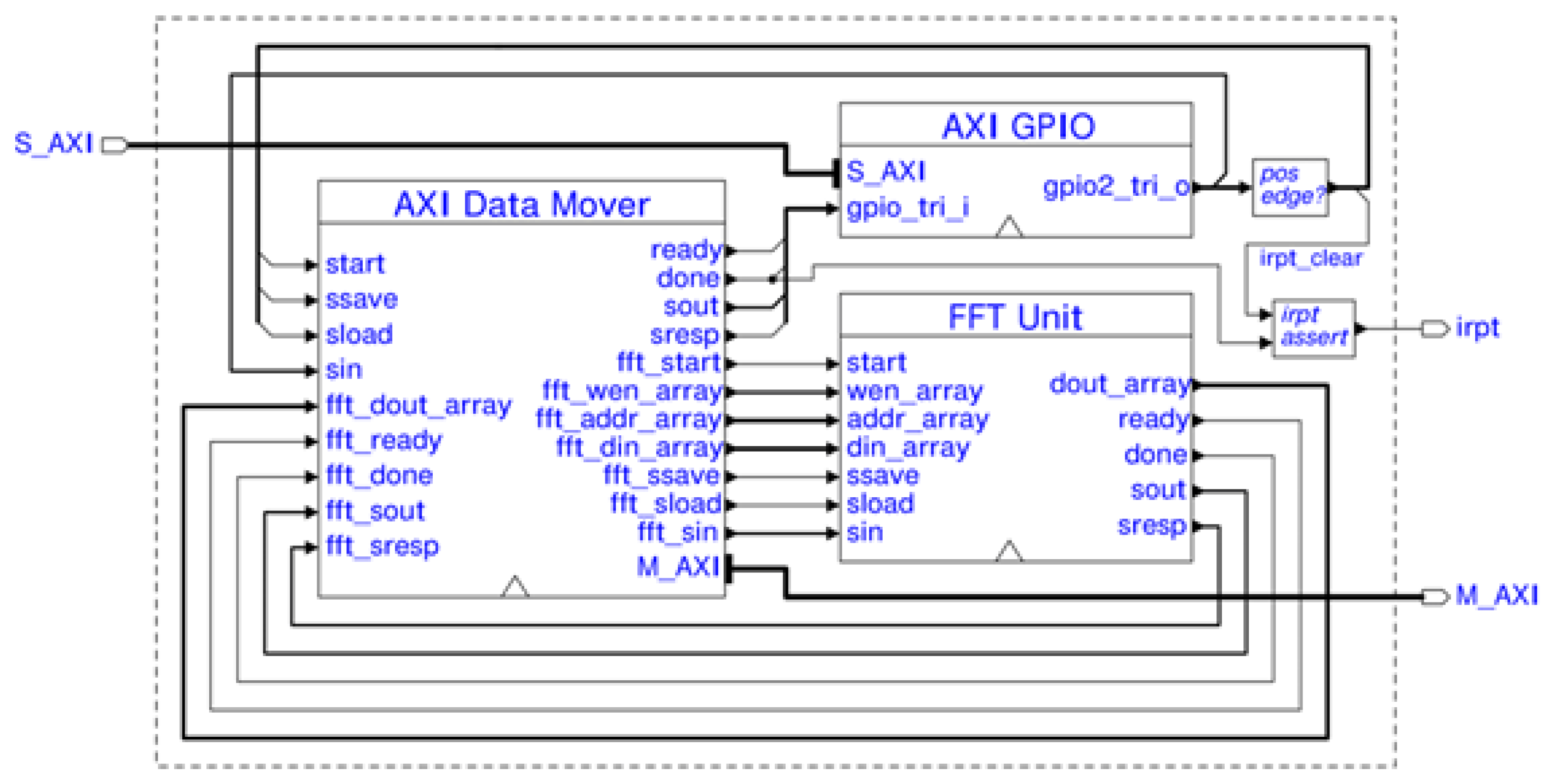
14]. AXI is a hardware communication protocol which in our case allows high speed data transfers between the PS and PL, as well as FFT control access from the PS by means of the AXI general purpose input/output (GPIO). The GPIO IP shown in
Figure 11 is provided by the FPGA vendor. The GPIO signals notify the PS to start the FFT calculation, manage FFT unit state saving and loading, and clear the co-processor interrupt.
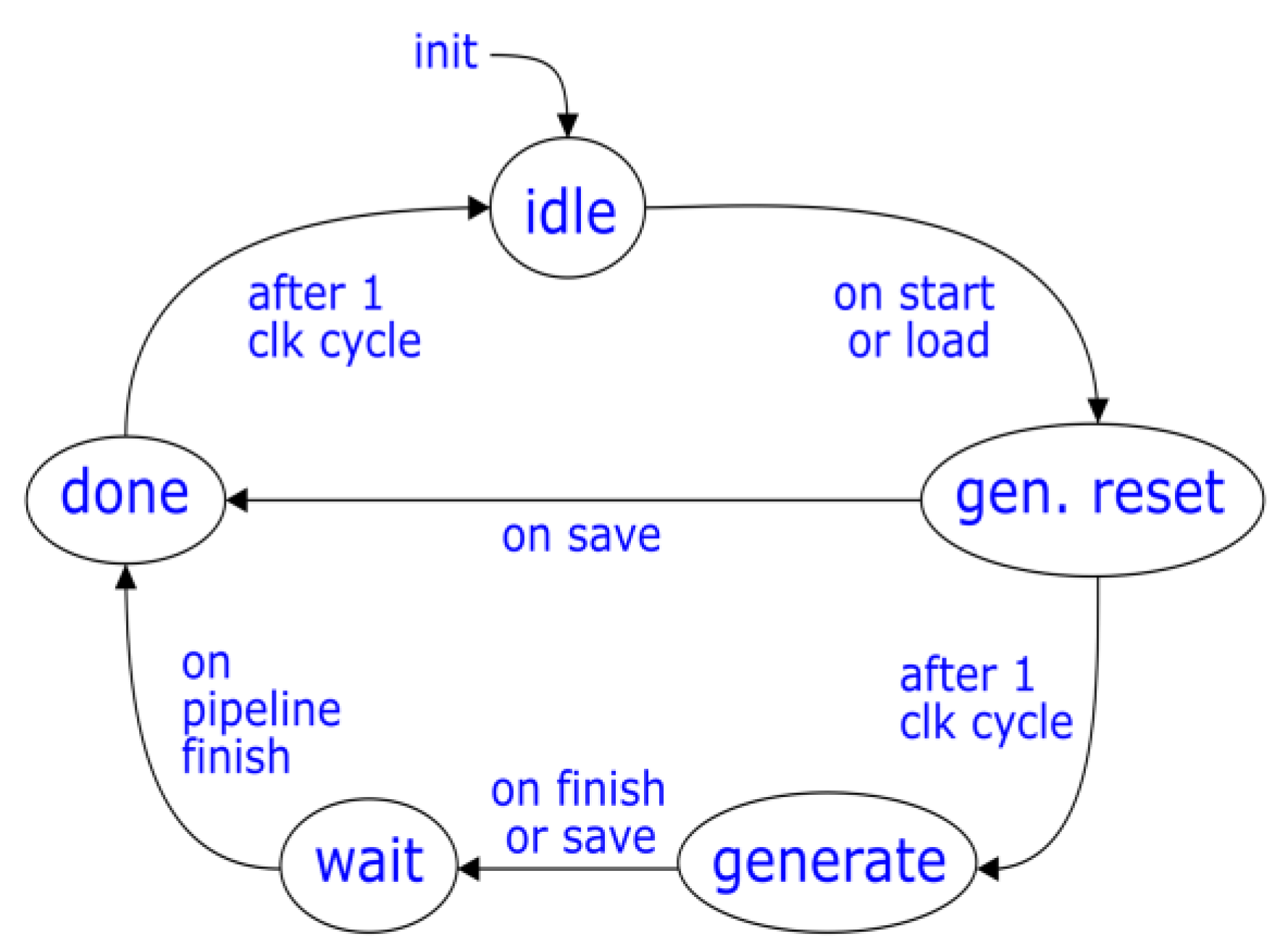
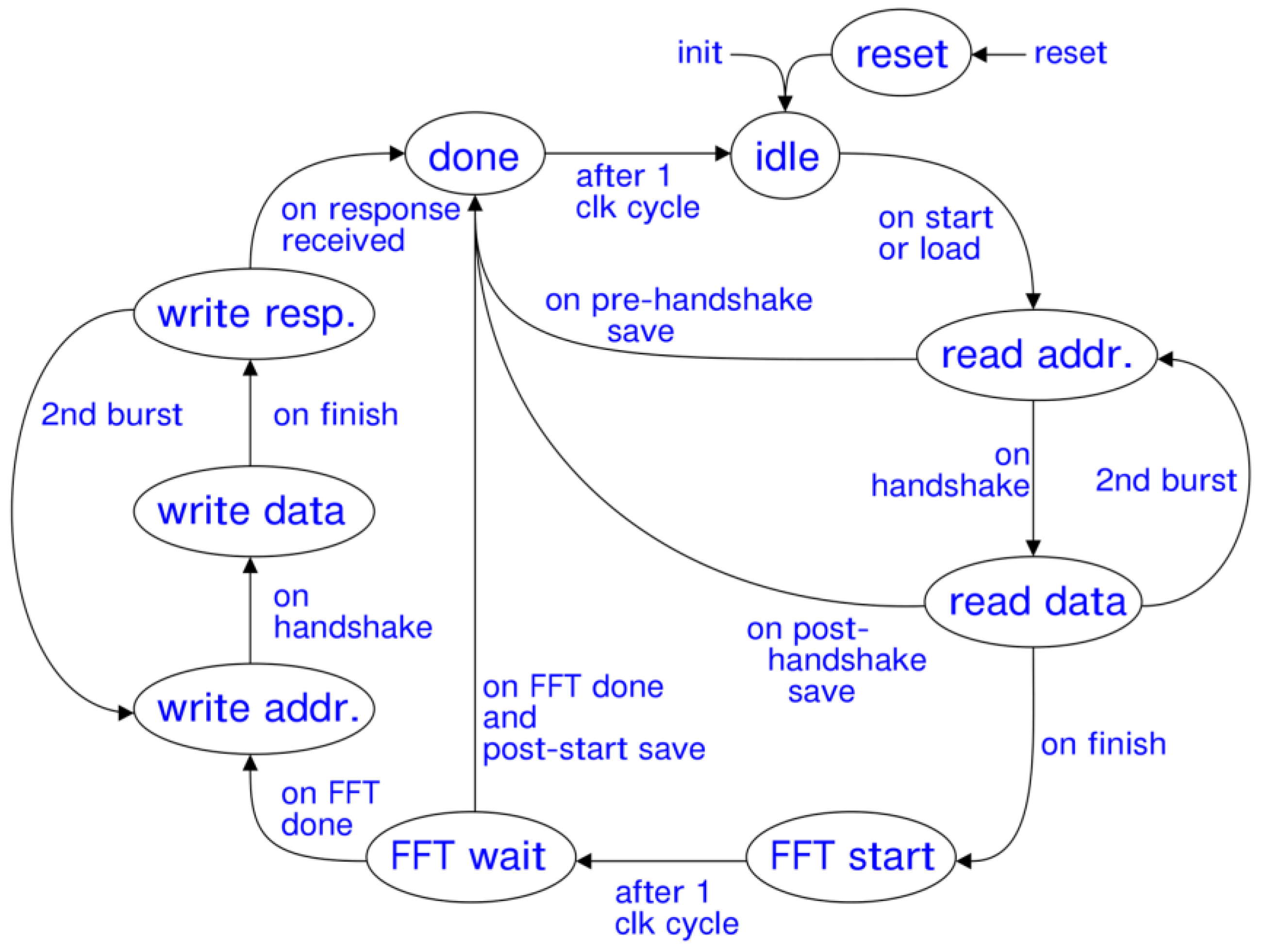
The AXI Data Mover makes use of an AXI master interface to move data between the FFT unit's RAM and an AXI slave. The FSM state graph of the Data Mover is shown in
Figure 12. When
start is pulsed, the AXI Data Mover reads data from the AXI slave and writes it to the FFT RAM, after which the FFT unit is started. Once the FFT unit signals
done, its RAM data is transferred to the AXI slave, finishing with the AXI Data Mover pulsing its own
done which raises the interrupt signal. The module is designed specifically for a 1024-point FFT with 32-bit data width (64-bit complex). Data reading and writing transfers are performed in two separate bursts due to the AXI protocol disallowing crossing of 4KB address boundaries (the mentioned FFT parameters imply 8KB data transfers).
The AXI Data Mover serves as a proxy for saving and loading FFT unit states, making use of practically the same signals ssave, sload, sin, sresp, and sout, the exception being sresp which is now one bit wide as opposed to two ('1' for valid, '0' for invalid i.e. FFT data is final). Upon saving, the AXI Data Mover takes care of interpreting the FFT unit's sresp and moving the FFT RAM data accordingly. Upon state loading, the AXI slave data is moved onto the FFT RAM and an FFT unit state load is performed. Accounted for is the fact that AXI transfers cannot be interrupted, and once an address handshake has been performed, the data transfer must be serviced to completion. Therefore, if a state save attempt occurs during a read address handshake or during a read data transfer, the state save will be taken care of after the data transfer has finished.
2.3. Reconfigurability
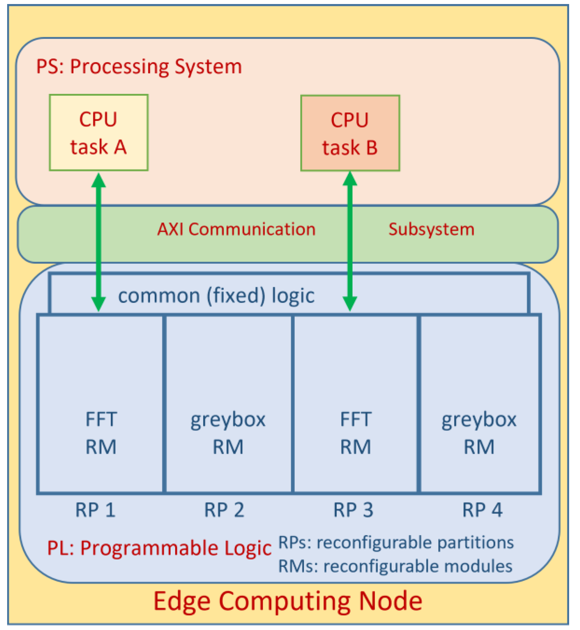
In the context of edge computing, the designed FFT co-processor and other potential co-processors must be hot-swappable with each other and with so-called “greyboxes” which are essentially blank modules. This is facilitated by a feature of the Zynq Ultrascale+ MPSoC PL called partial reconfiguration [
8] which, as the name states, allows for predetermined areas of the FPGA to be re-programmed whilst the rest remains unaffected. More details regarding this method are provided by [
9,
10]. The process involves the setup of “reconfigurable partitions” (RPs) which can be dynamically reconfigured to contain different so-called “reconfigurable modules” (RMs).
Figure 13 shows a setup with four such RPs.
For the FFT RM and other potential RMs to be configured onto the same RP, they must all share an interface so as to allow the RP instance to wrap around the RM. Our RP/RM interface was selected to contain the following elements:
a clock input signal
a reset input signal
an interrupt output signal
an AXI4 slave interface with 32-bit data width, 32-bit address width, and no user signals
an AXI4 master interface with 512-bit data width, 32-bit address width, and no user signals
The clock, reset, and interrupt signals speak for themselves when it comes to potential usage. The AXI slave is a narrow bus intended as a control path, used in our case to access the FFT Co-Processor's GPIO. The AXI master is a very wide bus intended as the data path. Four RP instances with the described interfaces make up the PL design seen in Fig 13. The PS of the Zynq UltraSCALE+ MPSoC in shown in more detail in
Figure 14. The clock and reset signals are shared among all RPs, whereas each RP has its own designated interrupt signal and AXI master and slave interfaces.
Partial bitstreams were generated for both the FFT Co-Processor and the greybox RM. A partial bitstream allows only one RP to be reconfigured as opposed to the entire PL. This means a total of 8 partial bitstreams were generated: 1 FFT Co-Processor partial bitstream and 1 greybox partial bitstream for each of the 4 available RPs. Along with the full bitstream which initial configured the PL, the partial bitstreams were written onto an SD card which made it possible for the PL to be partially configured by software.
3. Technical Results
In this chapter we look at some technical results. With an FPGA-based co-processor, what is of course important is the computing power achieved and the amount of resources that had to be used for it.
3.1. Achieved computing power
Two points of view need to be noted here. We have not optimized for the highest possible clock frequency. This would also depend on the FPGA technology. Therefore, for orientation purposes, we only indicate the number of clock periods that occur in the various processing steps. But when designing the clock-controlled processes, we did not pay attention to minimizing the number of cycles. What we were interested in was the principle of a co-processor that can be stopped to read its internal status or restarted with a specific status.
However, concentrating on pure computing power would not be correct with a co-processor, as there are latency times for data transfer. This results in the following data for normal accelerator operation:
Transferring the input data (operands) to the co-processor requires 135 clock cycles. This consists of a first so-called burst with 2 address and 65 data cycles followed by a second burst of the same duration. There is also an extra clock cycle to start the FFT calculation.
The computing time for a 1024-point FFT is 1295 clock cycles. This is because the 1024-point FFT is calculated in 10 stages and we carry out 512 butterfly operations per stage, for which in our case 4 butterfly units are available in parallel: i.e. (512/4)*10=1280 Clock cycles. In addition, there are 2 extra cycles for resetting the address generator and 11 extra cycles due to the processing pipeline.
It then takes 136 clock cycles to retrieve the results after the FFT calculation has been completed. Basically, the conditions here are the same as when transferring input data. However, we need 2 extra cycles for receiving the AXI write response.
In total, we use 1566 clock cycles for a complete co-processor run. If we use a conservative estimate of 100 MHz system clock, we end up with a processing time of around 16 µs. But we're not just interested in the pure processing time. After all, the reading of the co-processor status and the status reconstruction also have a time aspect.
149 clock cycles are used to stop the co-processor and then read the status. This is made up of the 136 clock cycles that we already know from normal readout and a delay of 13 additional clock cycles until the processing pipeline has been run through once. If the calculations have not yet started, we have a special case of 1 clock cycle.
However, loading the co-processor with a specific state requires 135 clock cycles, just like loading data in normal accelerator operation.
Overall, the question is justified as to whether, given such short calculation times, the effort involved in backing up and reconstructing a co-processor status is worth it and not simply setting up the calculation in the target edge node from scratch. But our aim here is to fundamentally research the feasibility of the method. In future work we will look for break-even points in this regard.
3.2. FPGA Implementation Details
Table 1 shows the PL resource requirements of a single FFT co-processor. It must be accounted for that up to four such units should fit on the PL at any one time, and that few additional resources are required for the static non-reconfigurable logic that surrounds the RPs. The resource utilization percentages are satisfactory in this regard, as they are quite distant from the <25% theoretical limit and therefore make floorplanning of the four RPs easier.
The design of the FFT co-processor reaches significant utilization percentages in distributed memory block (BRAM) and look-up-table (LUT) resources, with BRAM being decisively the highest. As the BRAM count would scale almost linearly with the FFT data point count, this means that the 1024-point FFT is the highest power-of-two data point count that our device could support for a four RP design. The high usage in both BRAMs and LUTs can mostly be attributed to the special multi-ported RAM unit [
17]. By contrast, very few of the available DSP units and flip-flops are used.
4. Discussion on Resource Consumption Versus Other Solutions
Table 2 showcases various FPGA-based FFT implementations and their resource requirements. Although data point counts and accuracy as well as the butterfly variant often differ from our proposed approach, some comparisons can still be made based on sensible assumptions. Our MPSoC's PL resources are used as reference for the percentage utilization values.
All approaches [
1,
13,
18,
19,
20] are unbalanced and show clear preferences for certain resource types. Our approach [
1] by comparison looks somewhat unfavorable, however we have taken no special measures to optimize the circuit synthesis. Our design also includes some slight overhead in the form of state management functionality.
In [
18], optimizations are performed in order to minimize the use of dedicated PL resources to the outcome that no DSPs are used, resulting on the other hand in high LUT and flip-flop requirements.
To more accurately judge our approach's BRAM utilization, we consider an alternative implementation with a similar data point count, i.e. 1024. For [
19], only 6 BRAM units are used to store the 16-bit data. Even considering our 32-bit data width, our BRAM requirements are still more than ten times greater.
The approach in [
20] declares minimizing distributed logic as a goal. It implements a radix-4 memory-based FFT and splits the 4096 data points at the input into 4 separate memories, and DSP unit usage is maximized. This results in 31 BRAMs and 98 DSPs total, which is a far more balanced result than ours.
Pipelined implementations are preferred for when throughput is of most importance. A 64 points FFT with 8 parallel radix-2 butterflies is designed in [
13]. A total of 48 DSP units are used, which considering double our number of butterflies still implies more optimizations with regards to DSP usage. BRAM requirements are not mentioned here.
Another approach described in [
21] does not document resource utilization, however, proves the advantages of using dedicated PL resources for speeding up 3D-FFT calculations.
RMs can only make use of the resources available inside the RP. Any RP resources that the configured RM does not use cannot be used for any other purposes. Therefore, when designing for partial reconfiguration, during floorplanning it must be ensured that an RP takes up at least as many resources required by its most demanding RM. By the same token, RMs must use the same reference as a resource utilization constraint. For optimal use of the RM's potential, idle resources should be avoided.
5. Conclusions and Future Work
Although our FFT unit provides a great deal of parallelism compared to more common single-pipeline implementations by performing four butterfly operations simultaneously, it does not make balanced use of the available PL resources. Following an approach such as in [
20] would greatly reduce resource requirements and improve balance and would potentially allow for faster clocking due to high DSP usage.
On a different note, our main goal was to design an example of a potential RM in the context of partial reconfiguration in edge computing applications. Our FFT co-processor can successfully interface with the software for purposes of control and data input/output through generic on-chip bus connectors and can save and restore calculation progress for use in state handover between edge nodes. To this extent, we have succeeded in developing an FFT RM which meets all the requirements for a potential partially reconfigurable edge node co-processor.
Regarding the FFT co-processor, in the next step we will adjust the algorithmic structure to achieve a better-balanced use of the PL resources. We will also expand the co-processor concept to other applications such as image processing or neural networks. On the software side, we will still be working on the handover mechanism.
Author Contributions
Peter Schulz: Conceptualization, Funding Acquisition, Investigation, Project administration, Supervision, Visualization, Writing – original draft, Writing – review and editing. Grigore Sleahtitchi: Investigation, Methodology, Software, Validation, Visualization, Writing – original draft, Writing – review and editing.
Funding
For performing the project described here, HAW Hamburg received funding from the Hamburg Innovation society, grant number C4T412.
Conflicts of Interest
The authors declare no conflict of interest and the funders had no role in the design of the study; in the collection, analyses, or interpretation of data; in the writing of the manuscript; or in the decision to publish the results.
References
- P. Schulz and G. Sleahtitchi, "FPGA-based Accelerator for FFT-Processing in Edge Computing," 2023 IEEE 12th International Conference on Intelligent Data Acquisition and Advanced Computing Systems: Technology and Applications (IDAACS), Dortmund, Germany, 2023, pp. 590-595. [CrossRef]
- R. Griessl et al., "Evaluation of heterogeneous AIoT Accelerators within VEDLIoT," 2023 Design, Automation & Test in Europe Conference & Exhibition (DATE), Antwerp, Belgium, 2023, pp. 1-6. [CrossRef]
- E. L. Chuma and Y. Iano, "Human Movement Recognition System Using CW Doppler Radar Sensor with FFT and Convolutional Neural Network," 2020 IEEE MTT-S Latin America Microwave Conference (LAMC 2020), Cali, Colombia, 2021, pp. 1-4. [CrossRef]
- P. Schulz: "Antrag auf Gewährung einer Zuwendung im Rahmen der Fördermaßnahme Call for Transfer", internal document, unpublished, 20, (in German).
- Y. Cao and Y. Chen, "QoE-based node selection strategy for edge computing enabled Internet-of-Vehicles (EC-IoV)," 2017 IEEE Visual Communications and Image Processing (VCIP), St. Petersburg, FL, USA, 2017, pp. 1-4. [CrossRef]
- L. Ma et al., “Efficient Service Handoff Across Edge Servers via Docker Container Migration,” Proceedings of Symposium on Edge Computing, San Jose, CA, Oct. 2017.
- T. Hill: "Advancing the Use of FPGA Co-Processors through Platforms and High-Level Design Flow", White Paper, Xilinx WP394, 2011.
- C. Kohn: "Partial Reconfiguration of a Hardware Accelerator with Vivado Design Suite for Zynq-7000 AP SoC Processor", Application Note, XAPP1231, 2015.
- Z. Zhu et al., "A Hardware and Software Task-Scheduling Framework Based on CPU+FPGA Heterogeneous Architecture in Edge Computing," in IEEE Access, vol. 7, pp. 148975-148988, 2019. [CrossRef]
- M. Monopoli, L. Zulberti, G. Todaro, P. Nannipieri and L. Fanucci, "Exploiting FPGA Dynamic Partial Reconfiguration for a Soft GPU-based System-on-Chip," 2023 18th Conference on Ph.D Research in Microelectronics and Electronics (PRIME), Valencia, Spain, 2023, pp. 181-184. [CrossRef]
- G. Slade: “The Fast Fourier Transform in Hardware: A Tutorial Based on an FPGA Implementation”, published on ResearchGate https://www.researchgate.net/publication/235995761, March 2013, retrieved in May 2023.
- Z. A. Abbas, N. B. Sulaiman, N. A. M. Yunus, W. Z. Wan Hasan and M. K. Ahmed, "An FPGA implementation and performance analysis between Radix-2 and Radix-4 of 4096 point FFT," 2018 IEEE 5th International Conference on Smart Instrumentation, Measurement and Application (ICSIMA), Songkhla, Thailand, 2018, pp. 1-4. [CrossRef]
- S. Mookherjee, L. DeBrunner and V. DeBrunner, "A low power radix-2 FFT accelerator for FPGA," 2015 49th Asilomar Conference on Signals, Systems and Computers, Pacific Grove, CA, USA, 2015, pp. 447-451. [CrossRef]
- “UltraScale Architecture and Product Data Sheet: Overview”, AMD/Xilinx product specification document, Ref. No. DS890 (v4.4), June 22, 2023.
- Trenz, “TE0818starter kit”. https://wiki.trenz-electronic.de/display/PD/TE0818+Resources, retrieved December 2023.
- G. Sleahtitchi: "FPGA on the Edge” internal project reports, unpublished, Dezember 2021.
- C. E. LaForest and J. G. Steffan: “Efficient multi-ported memories for FPGAs”, Proceedings of the 18th annual ACM/SIGDA international symposium on Field programmable gate arrays (FPGA '10), p. 41–50, Association for Computing Machinery, New York, NY, USA, 2010.
- T. Belabed, S. Jemmali and C. Souani, "FFT implementation and optimization on FPGA," 2018 4th International Conference on Advanced Technologies for Signal and Image Processing (ATSIP), Sousse, Tunisia, 2018, pp. 1-6. [CrossRef]
- S. Ranganathan, R. Krishnan and H. S. Sriharsha, "Efficient hardware implementation of scalable FFT using configurable Radix-4/2," 2014 2nd International Conference on Devices, Circuits and Systems (ICDCS), Coimbatore, India, 2014, pp. 1-5. [CrossRef]
- M. Garrido, M. Á. Sánchez, M. L. López-Vallejo and J. Grajal, "A 4096-Point Radix-4 Memory-Based FFT Using DSP Slices," in IEEE Transactions on Very Large Scale Integration (VLSI) Systems, vol. 25, no. 1, pp. 375-379, Jan. 2017. [CrossRef]
- B. S. C. Varma, K. Paul and M. Balakrishnan, "Accelerating 3D-FFT Using Hard Embedded Blocks in FPGAs," 2013 26th International Conference on VLSI Design and 2013 12th International Conference on Embedded Systems, Pune, India, 2013, pp. 92-97. [CrossRef]
| 1 |
The project was funded by Hamburg Innovation. Funding code: C4T412 [1] |
|
Disclaimer/Publisher’s Note: The statements, opinions and data contained in all publications are solely those of the individual author(s) and contributor(s) and not of MDPI and/or the editor(s). MDPI and/or the editor(s) disclaim responsibility for any injury to people or property resulting from any ideas, methods, instructions or products referred to in the content. |
© 2024 by the authors. Licensee MDPI, Basel, Switzerland. This article is an open access article distributed under the terms and conditions of the Creative Commons Attribution (CC BY) license (http://creativecommons.org/licenses/by/4.0/).
