1. Introduction
RFID (Radio Frequency Identification) systems are used in a variety of fields, including logistics, item level inventory tracking, access control, race timing, tool tracing, materials management [
1,
2] with new applications currently appearing, e.g. health related ones [
3]. RFID tags may be classified into active, semi-passive, and passive ones. Active RFID tag uses a power supply and a transmitter for communication; a semi-passive RFID tag has a power source but no transmitter. Passive RFID tag functions using the electromagnetic field power delivered by the reader, so it is the cheapest option. Typical frequency bands for RFID applications include 125/135 KHz (LF), 13.56 MHz (HF), 433 MHz and 840 - 960 MHz (UHF) and 2.45 and 5.8 GHz in the microwave region [
4].
Numerous studies [
5,
6] have explored Si based designs for OCA (On Chip Antennas) with a view to improving gain and efficiency and reducing parasitic interconnections. Such antennas generally tend to have narrow bandwidth (less than 10%) and a limited radiation efficiency and range, but what distinguishes them is their small size, allowing integration into a variety of electronic devices [
7]. Recent developments in implementation of high-performance on-chip antennas for millimeter wave and terahertz integrated circuit applications are discussed in [
8,
9]. On-chip antennas show significant potential to accommodate applications in fields such as 5G, Internet of Things (IoT), autonomous vehicles, high data rate point-to-point communications, GPS, WiFi, WLAN, Bluetooth and wireless sensors. Recent studies [
9] show a promising new approach using novel substrate layers such as silicon, graphene, polyimide and GaAs to facilitate IC integration, as well as a new excitation mechanism that appears to suppress the propagation of surface waves and reduce substrate loss.
In this work, a RFID design on a Si based structure is studied, with a view to improvements in impedance matching, bandwidth and gain performance. The main motivation is to achieve a configurable design of an RFID tag antenna on Si. With the parameterized option, one can easily change the total area of the design and consequently the frequency region, by changing only one dimension, and subsequently modify it as specific needs arise. The coupling between the design lines can be controlled by varying the distance between the lines. In this work, the focus is on the design of an RFID antenna at 2.4GHz and 5.8GHz. These frequencies have been chosen because of substantial current demand for multi-frequency components in a variety of applications (WiFi, Bluetooth, IoT, etc) that may be expected to further increase in the near future.
2. Antenna Design
The RFID antenna design under consideration, as presented in more detail in [
10], will be briefly outlined here.
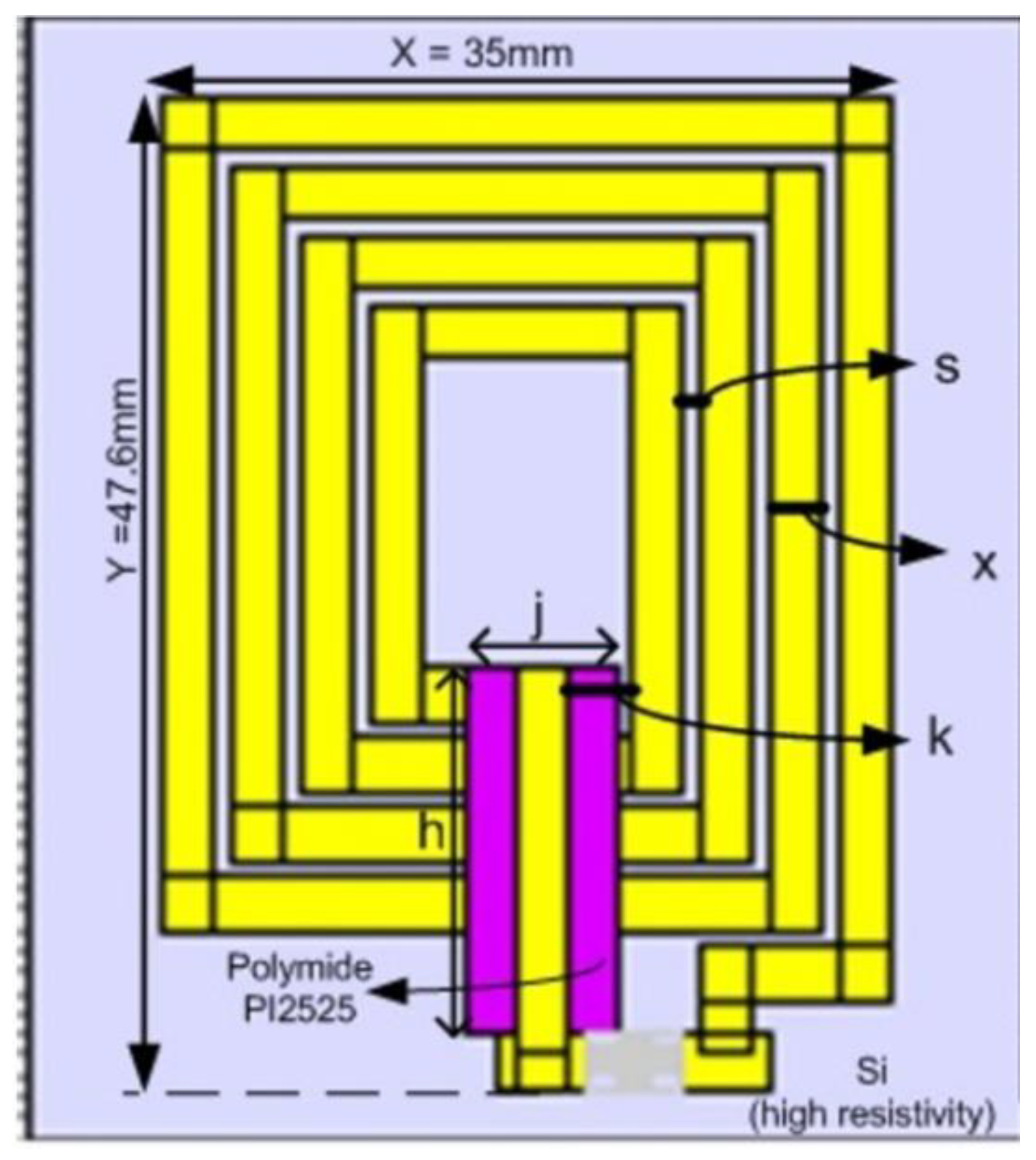
Figure 1 and
Figure 2 depict the substrate structure (cross section) and the corresponding antenna layout (top view). Following an iterative design process, a set of values for the design dimensions has been selected [
10] and used for simulation and fabrication of the antenna as follows.
The substrate material for the design is Si (high resistivity) and Polyimide PI2525 for the bridge dielectric. The dielectric constant εr for high resistivity Si is 11.68 and for PI2525 is 2.68. In
Figure 1, b
sub is 0.320 mm, b
cop (thickness of copper plates) is 3 μm, bsp is 0.018 mm and b
dielectric is 3 μm. The total area of the antenna component (a) is 35 x 47.6 mm
2. The spacing (s) and width (x) of the spiral lines, as shown in
Figure 2, are 0.85 mm and 2.5 mm, respectively, and h and j are 17.6 mm and 7.5 mm, respectively.
The antenna operation is based on electromagnetic coupling since the presence of an incident electromagnetic field on the antenna will create a magnetic field due to the coupling between the lines ([
11] pp 1-2). Decrease of the gap between the lines corresponds to stronger electromagnetic coupling between them.
For the parameterized design the following formulas have been used:
where N is the number of turns and
, where i = 0:3 with step 1,
, where i = 1:3 with step 1,
, where j = 0:3 with step 1,
, where j = 1:3 with step 1,
for , i = 0:3 with step 1 and for , j = 0:3 with step 1
Equations (1) and (2) are the basic conditions for creating the spiral antenna shown in
Figure 2. N corresponds to the number of turns and M corresponds to the number of spaces between the metal paths (In
Figure 2, M=3). We note that equation (1) refers to x dimension and (2) to the y dimension, with
,
, respectively, where X and Y are the maximum dimensions. We use (1) and (2) for each metal path. For the first inner metal path we apply a correction parameter
when
.
The substrate thickness is also taken into account in (1), (2) through the CST calculations, for the z axis. Equations (1), (2), (3) determine the design and lead to the final design of a parameterized antenna through a series of CST simulations. To optimize the value, repeated parametric simulations were performed.
The inductance is calculated by the following equations (see e.g. [
12] pp. 95-96):
We use these equations, especially (5a) and (5b), for each one of 19 metal paths in total. As already has been mentioned, the values of x (width) and s (space) for the lines, as shown in
Figure 2, have been specifically selected for optimization of the S
11 parameter at the frequencies of interest.
3. Simulation Results
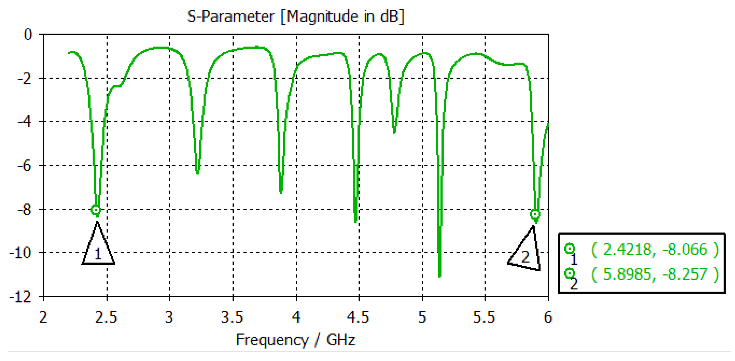
Figure 3 shows results of numerical simulation for the reflection coefficient
at the antenna driving point, plotted versus frequency. Some dips (quasi-resonant frequencies) with
about – 7 dB or better are observed in the region between 2.2 and 6 GHz. The dip frequencies, besides 2.4 and 5.9 GHz, are approximately 3.2 GHz, 3.9 GHz, 4.4 GHz, 4.7 GHz and 5.2 GHz. The dips’ position and depth depend upon several design parameters, including s (spacing), x (width) and bcop (thickness of copper). Some simulation results for the frequencies of 2.4 GHz and 5.8 GHz are summarized in
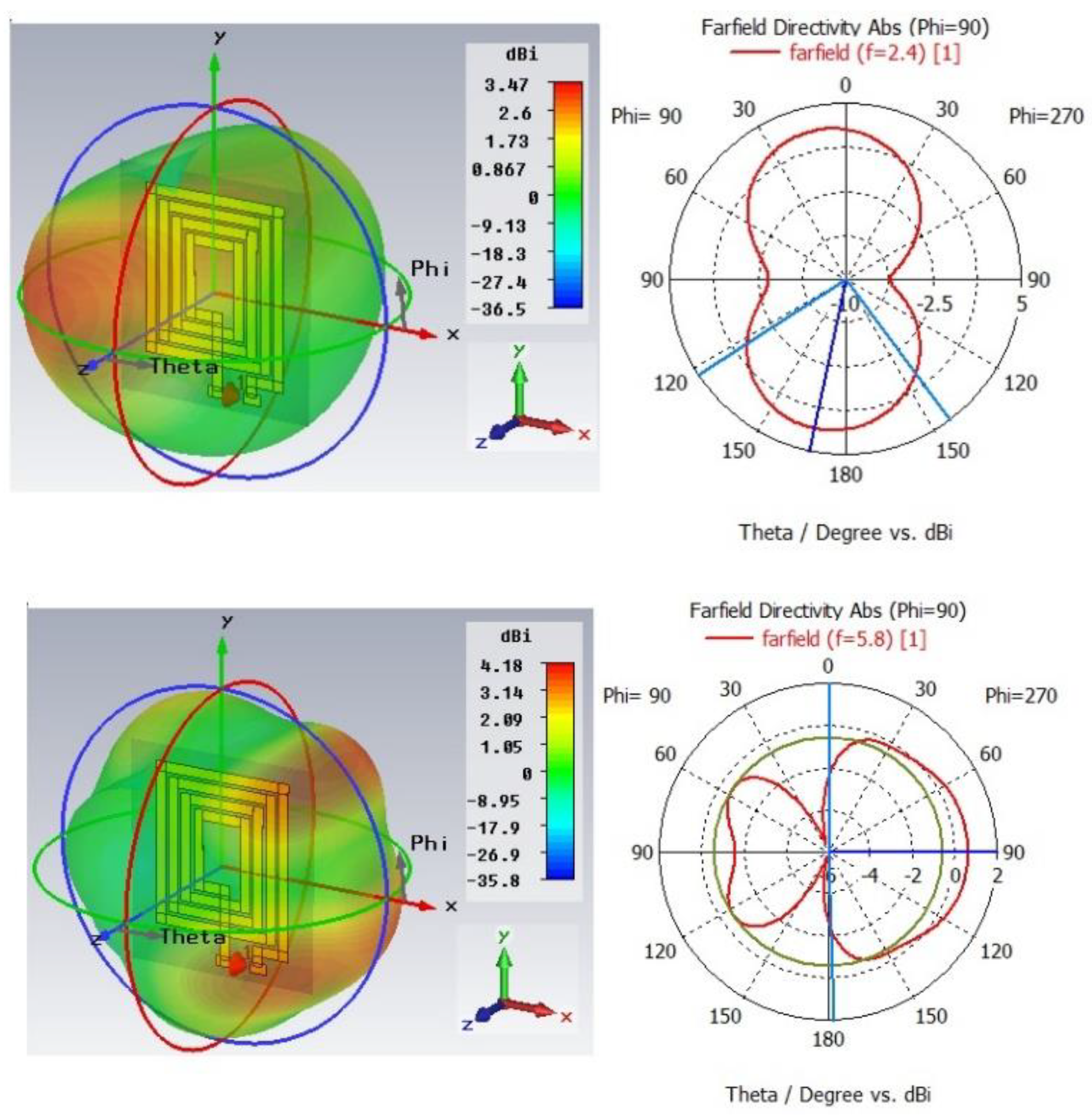
Table 1, including the antenna maximum directivity (3.47 dBi and 4.18 dBi, respectively). Detailed far field results and polar patterns are shown in
Figure 4a,b. In both frequencies of interest, the antenna radiation pattern is quite broad. At 2.4 GHz (
Figure 4a), it comprises two almost symmetric wide lobes around the z-axis in the φ = 90
o, 270
o plane. At 5.8 GHz (
Figure 4b), a frontal lobe and a somewhat smaller backward lobe are observed around the x-axis.
4. Fabrication and Testing
4.1. Fabrication
An RFID tag antenna specimen was fabricated at the microelectronics laboratory of Foundation for Research and Technology - Hellas and tested at the telecommunications laboratory of Hellenic Naval Academy. The microfabrication process involves steps of metallic structure pattern transfer techniques including optical UV lithography procedures (for the pattern transfer of CAD layout designed patterns), metal depositions using electroplating and spin-coated stay-on dielectrics.
The procedure begins with the standard degreasing of a Silicon substrate (76 mm / 3 inches in diameter), which is a Float-Zone (FZ) Silicon, with a wafer thickness of 380 μm, crystallographic orientation of (100) and, most importantly, high resistivity of 10000-1000000 Ohm cm (like a pure dielectric substrate). The degreasing step is a standard organic solvent cleaning procedure with ultrasonic-agitated dipping of the Si substrate in the following order: Acetone, Isopropanol, and finally deionized H2O. The substrate is dried using nitrogen. Following this step, the AZ 9260 resist is spin coated with a thickness of 0.006 mm onto the substrate and thermally stabilized using a hot plate at 110oC for 2 min. The transfer pattern is done by exposing the layout mask of the bottom inductor spiral using i-line UV lithography with the mask aligner Suss MA6 and developing the exposed photoresist with the use of AZ826MIF developer.
The bottom inductor spiral electrode of the RFID is metalized with 3 μm thick copper (Cu) electroplating using the previous lithography. As a dielectric “bridge” support for the bridge interconnect that is intended to connect the center of the spiral coil to the outside electrode, the spin-on polyimide dielectric PI2525 is used. Directly above the polyimide layer, another photoresist layer is spin coated. The previous optical lithographic technique is once more used to define and transfer the pattern of the dielectric bridge support with the co-development of both the photoresist and the underlying polyimide layer. After the selective resist stripping of the photoresist mask, the polyimide is stabilized by a thermal treatment curing procedure on a programmable hot plate with a ramping heating from room temperature up to 350oC in ambient nitrogen atmosphere.
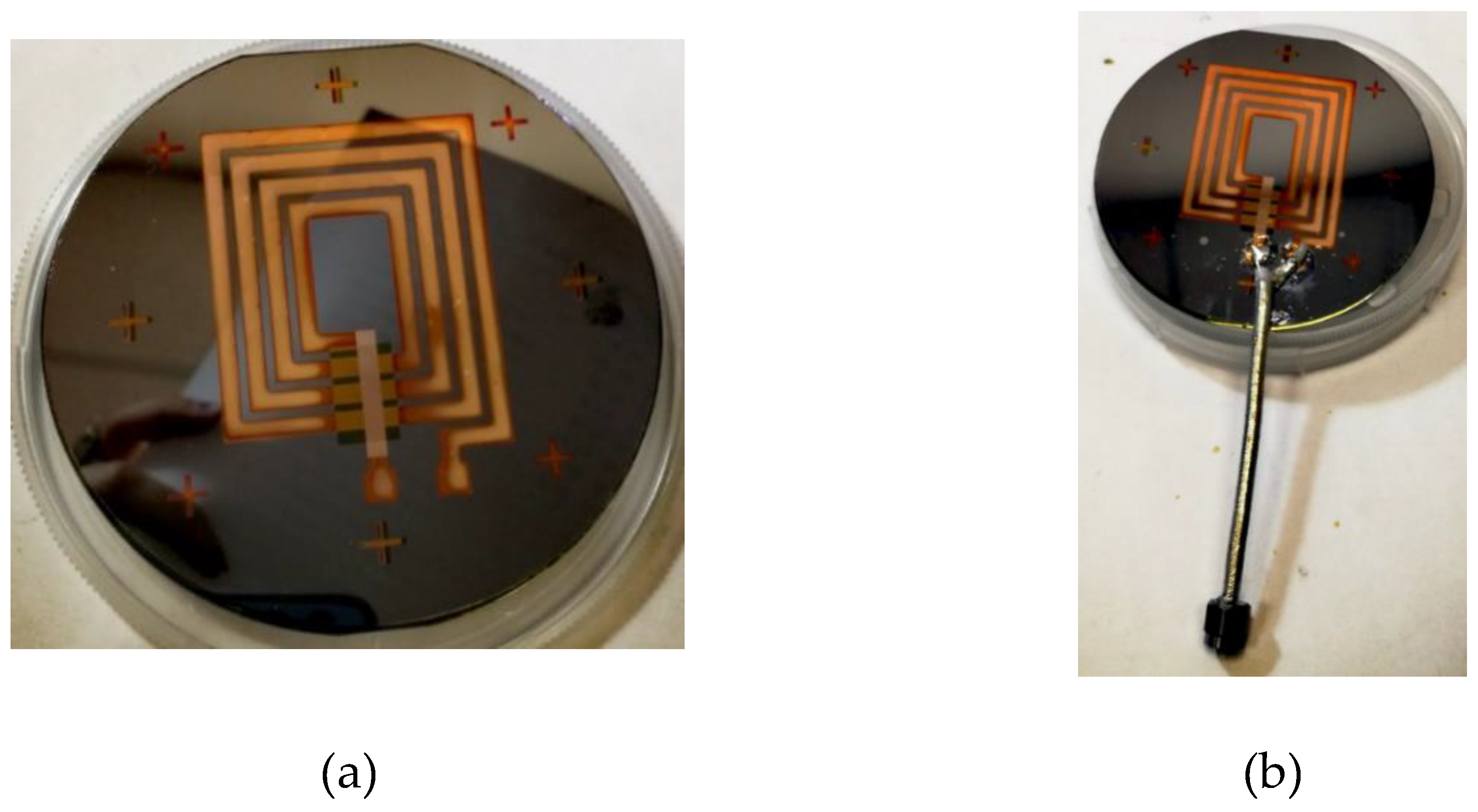
Finally, similar to the first lithographic patterning and Cu electrodeposition process, the bridge Cu interconnect, with a thickness of 5 μm, is realized in order to electrically connect the inner core part of the bottom spiral inductor with the outer electrode. The fabricated RFID is presented in
Figure 5 &
Figure 6.
4.2. Test Setup
The reflection coefficient and gain of the fabricated RFID antenna was measured with a PicoVNA 106 Vector Network Analyzer (VNA) over the instrument’s frequency range of up to 6 GHz. To this end, an SMA connector was attached (as shown in
Figure 5) to the input pads of the RFID antenna via a small piece (10 cm approx.) of 50-ohm coaxial cable of RG400 type. The SMA input port thus obtained was connected to the VNA port 1 test lead to measure the reflection coefficient
. The transmission coefficient
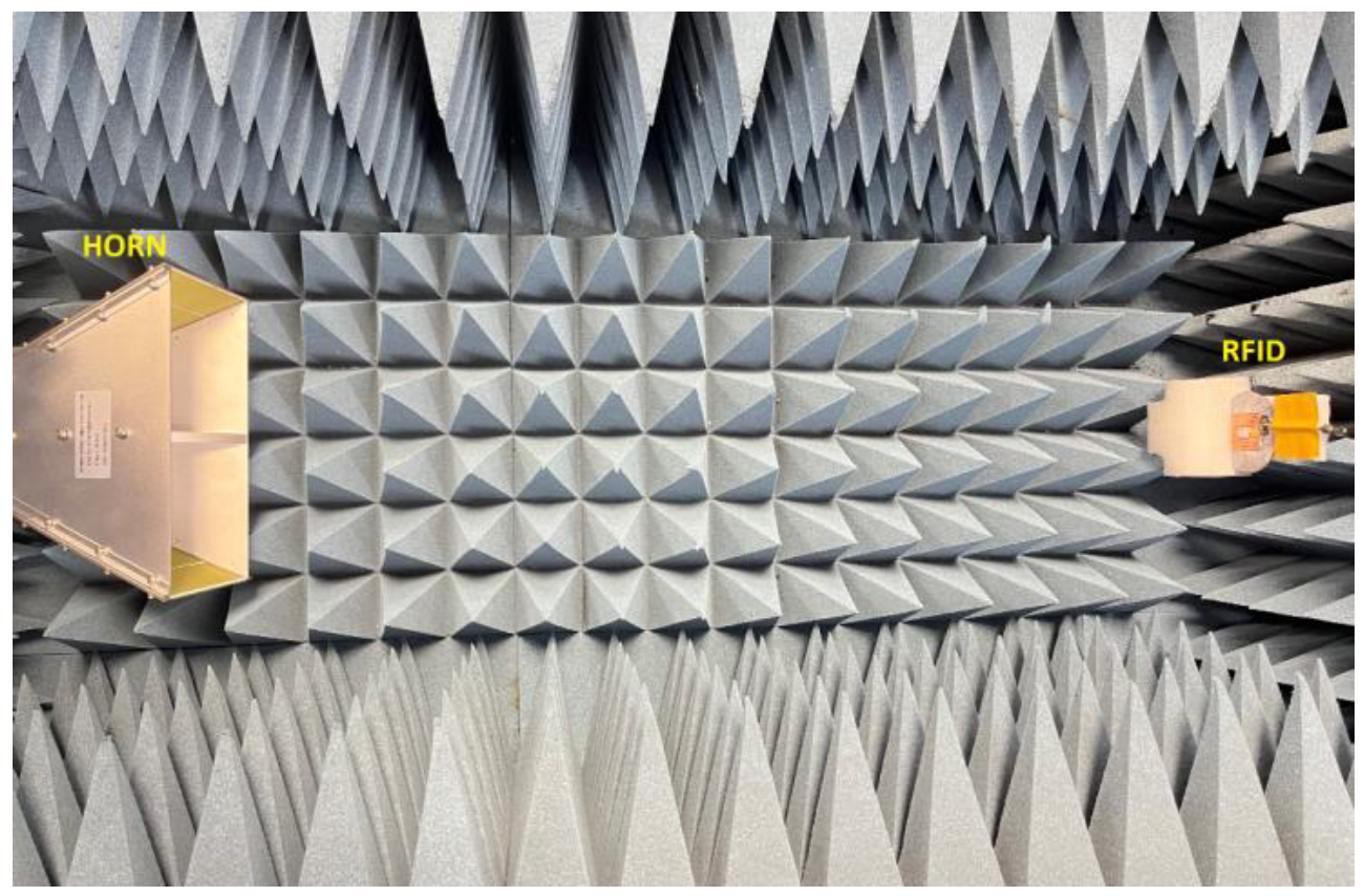
was subsequently measured connecting a wideband dual-ridged TEM horn antenna (Vector Telecom Part No VT10180DRHA10SK) to the second VNA port test lead (
Figure 6a). The horn antenna is rated, according to specifications, at a maximum VSWR of 2.5 and an average gain of 10 dB over the 1 – 18 GHz frequency range. Calibration of the VNA was carried out by the standard SOLT method at the test leads, using its accompanying mechanical calibration kit (furnished by the manufacturer). Measurement of
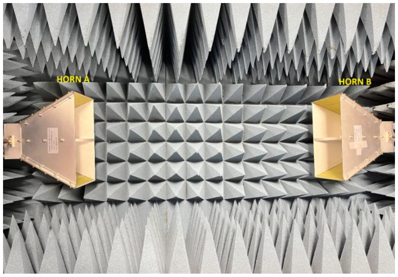
was repeated for two identical horn antennas of the same type, connected to the same VNA test leads (
Figure 6b). In all cases, the antennas were placed inside an anechoic enclosure of dimensions about 150 × 90 × 60 cm. For mechanical support, expanded polystyrene was used to minimize multiple scattering effects inside the enclosure.
Using the well-known Friis transmission equation (see e.g. [
11] pp. 86-88), and taking into account the antenna input mismatch losses, we obtain the following for the gain
of the horn antennas and subsequently for the gain
of the RFID antenna
where
and
and
are the S-matrix transmission coefficient values measured for the two configurations of
Figure 6a,b.
Obviously, (7–8) represent a simplified version of the well-known three-antenna method, considering two identical horns. The validity of the simplification was verified by interchanging the two horns transmitting towards the RFID tag antenna and observing very close results for the transmission coefficient. Both and incorporate, via (9), the mismatch losses at the test lead ports connecting the horns and the RFID antenna (hence the primed notation). The effect of insertion and mismatch losses along the test leads is compensated by calibration of the VNA at the test lead ports. Thus, the value of the gain of the RFID antenna is obtained via (9). To compensate for the insertion loss of the small coaxial cable stub attached to the input pads of the RFID antenna, the insertion loss was measured for a cable of the same type and length with SMA connectors at both ends. A value of approximately 0.2 dB was found and added to the results of (9).
To calculate directivity from measured gain values for comparison with the simulated ones, the radiation efficiency of the RFID tag specimen was measured at frequencies of 2.4 and 5.8 GHz, using the classic Wheeler Cap method [
13,
14,
15]. The antenna under test was placed in a cylindrical box (tin can) of approximately 9.7 cm diameter and 6 cm height, covered with a circular aluminum lid with a small opening for the antenna feed coaxial cable. According to the findings of [
14], care was taken to ensure good electrical contact between the box and the lid, and to place the specimen as near the center of symmetry of the box as possible. Using the same VNA (PicoVNA 106) with test leads and calibration data as above, the complex reflection coefficient
was measured. The measured value was subsequently transformed by rotation along a lossless transmission line, as suggested in [
15], to achieve a good approximation of the antenna input impedance via a series equivalent circuit. Taking the real part of the input impedance, calculated from
, as the loss resistance, the radiation efficiency of the tag specimen is given by the standard Wheeler Cap formula [
14]
where
and
are the input impedances without and with the cap, respectively. It was verified that
at both frequencies of interest, i.e. the measured values are consistent with the underlying assumption of a series equivalent circuit for the antenna under test.
4.3. Testing Results
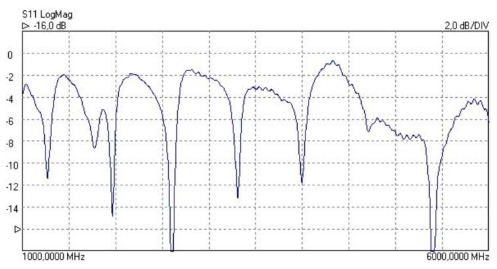
Measured
values for the RFID tag are shown in
Figure 7, bearing a close similarity with the simulated values of
Figure 3.
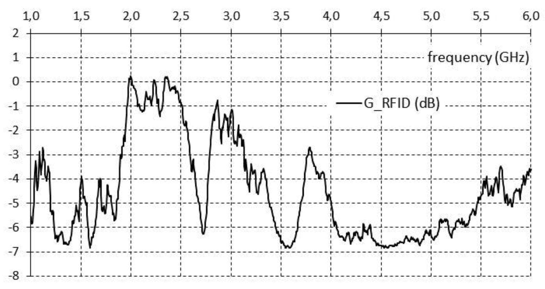
Measured results for the gain
of the RFID antenna are shown in
Figure 8. In all, they are several dB lower than the simulated directivity values, especially in the region of 5.8 GHz. The difference is probably due to significant resistive losses over the RFID antenna structure; such losses are to be expected in printed antennas to a greater extent than wire antennas, while larger losses at higher frequencies are usually due to skin effect. As a check, the radiation efficiency measurements (described above) at 2.4 and 5.8 GHz give efficiency values of
= 0.85 and 0.6 respectively, corresponding to differences of 0.7 and 2.2 dB between the directivity and gain values at these frequencies.
5. Discussion and Conclusions
Upon comparison of the simulated and measured results for the
as shown in
Figure 3 and
Figure 7, it may be seen that the measured dip frequencies are close to the simulated ones, with the exception of the vicinity of 5.8 GHz where no dip is found but the measured
value remains below – 4 dB. On the other hand, the dip near 2.4 GHz is displaced to the right, as compared with the simulated results, but the measured
value at 2.4 GHz is about – 3.6 dB. In future practical applications, a transmission line segment could be fabricated on the same substrate between the antenna pads and the input terminal, adjusting the parameters s and x (
Figure 2) and possibly including matching components as appropriate to further improve reflection losses. The measured gain (
Figure 8) exhibits peaks near the frequencies of interest (mainly 2.4 and 5.8 GHz), while maintaining considerable stability around both frequencies of interest, along with a large beamwidth around broadside direction (Table 2). As already noted, the measured gain values indicate significant losses on the antenna, which appears to be confirmed by efficiency measurement using the Wheeler cap technique. In all, simulated and measured values in good agreement demonstrate promising characteristics of the proposed RFID design for a variety of applications.
Author Contributions
Conceptualization, T.K. and A.A.; Data curation, T.K., C.V. and C.B.; Formal analysis, T.K. and C.V.; Funding acquisition, C.V.; Investigation, T.K., C.V. and C.B.; Methodology, T.K., C.V. and A.A.; Resources, C.V., A.S. and G.S.; Supervision, C.V.; Validation, C.V.; Visualization, T.K.; Writing – original draft, T.K.; Writing – review & editing, C.V. All authors have read and agreed to the published version of the manuscript.
Funding
This research was funded by Microelectronics Research Group, Institute of Electronic Structure and Laser, Foundation for Research and Technology, Univercity of Crete 70013, Vassilika Vouton, Herakleion, Crete, Greece.
Acknowledgments
We acknowledge support of this work by the project “National Research Infrastructure on nanotechnology, advanced materials and micro/nanoelectronics “(MIS 5002772) which is implemented under the “Action for the Strategic Development on the Research and Technological Sector” and the project T1EDK-00329 under the call RESEARCH – CREATE – INNOVATE funded by the Operational Programme "Competitiveness, Entrepreneurship and Innovation" (NSRF 2014-2020) and co-financed by Greece and the European Union (European Regional Development Fund).

References
- Khalifeh A., Khalid A. “Wireless Sensor Networks for Smart Cities: Network Design, Implementation and Performance Evaluation”, MDPI, January 2021, volume 10. [CrossRef]
- Zayoud R., Besbe M., “Agricultural and Environmental Applications of RFID Technology”, International Journal of Agricultural and Environmental Information Systems, April 2014, volume 5. [CrossRef]
- Elsheakh D., Ahmed M., “Rapid Detection of Coronavirus (COVID-19) Using Microwave Immunosensor Cavity Resonator”, MDPI, October 2021, volume 21. [CrossRef]
- Prakash P.,Durga P.,“Design of a Chipless RFID Tag for 2.4 GHz and 5.8 GHz ISM Band Applications”, IEEE International Students' Conference on Electrical, Electronics and Computer Science, February 2020.
- Lin J., Wu H., “Communication Using Antennas Fabricated in Silicon Integrated Circuits”, IEEE, August 2007, Volume 42, pp.1678 - 1687. [CrossRef]
- Dhillon A., “An Analysis of RF On-Chip Antennas in Si-Based Integrated Microwave ,Photonics”, IEEE, April 2021, volume 13. [CrossRef]
- Kantareddy S.N., Mathews I., "Perovskite PV-Powered RFID: Enabling Low-Cost Self-Powered IoT Sensors.", IEEE Sensors Journal, January 2020, Volume 20, pp. 471 – 478. [CrossRef]
- Althuwayb AA, Al-Hasan M., “Design of half-mode substrate integrated cavity inspired dual-band antenna”, International Journal of RF and Microwave Computer-Aided Engineering, December 2020, volume 31. [CrossRef]
- Alibakhshikenari M., Ali E.M., “A Comprehensive Survey on Antennas On-Chip Based on Metamaterial, Metasurface, and Substrate Integrated Waveguide Principles for Millimeter-Waves and Terahertz Integrated Circuits and Systems”, IEEE Access, January 2022, volume 10, pp.3668 – 3692.
- Korfiati T., Karagianni E., “Configurable Multi-Frequencies Microstrip Square Spiral Antenna RFID Tag at S abd C – Band with different substrates”, Proc. 9 IC – EPSMO, Athens, July 2021, pp. 108-113.
- Balanis C.A., “Antenna Theory, Analysis and Design”, 2nd edition, John Wiley & Sons: Ney York, USA, 1997.
- Jia-Sheng Hong, M.J.Lancaster, “Microstrip Filters for RF Microwave Aplications”, John Wiley and Sons, 2001.
- Wheeler, H.A., “The radiansphere around a small antenna”, Proc. IRE, August 1959, pp. 1325 –1331.
- Pozar, D.M., Kaufman, B., “Comparison of three methods for the measurement of printed antenna efficiency”, IEEE Trans. Antennas Propagat., no. 1, January 1988, volume 36, pp. 136 –139. [CrossRef]
- McKinzie III, W.E., “A modified Wheeler cap method for measuring antenna efficiency”, Proc. IEEE Int. Antennas and Propagat. Symposium, 1997, volume 1, pp. 542 –545. [CrossRef]
|
Disclaimer/Publisher’s Note: The statements, opinions and data contained in all publications are solely those of the individual author(s) and contributor(s) and not of MDPI and/or the editor(s). MDPI and/or the editor(s) disclaim responsibility for any injury to people or property resulting from any ideas, methods, instructions or products referred to in the content. |
© 2024 by the authors. Licensee MDPI, Basel, Switzerland. This article is an open access article distributed under the terms and conditions of the Creative Commons Attribution (CC BY) license (http://creativecommons.org/licenses/by/4.0/).


