1. Introduction
The quality of the surface of silicon carbide (SiC) wafers significantly impacts the performance of electronic devices. Therefore, a smooth and defect-free surface is essential for SiC wafers [
1]. When SiC ingot are sliced into substrate, surface cracks and damage become pronounced [
2]. Traditional methods involve lapping and polishing to eliminate surface defects, with a final requirement of achieving a surface roughness of 0.5 nm. However, due to the high hardness, brittleness, and chemical stability of SiC, traditional processes exhibit low efficiency and high costs [
3]. Consequently, there is a need to develop new surface processing technologies for the rapid treatment of sliced SiC surfaces. Femtosecond laser surface polishing technology offers advantages such as non-contact operation, low thermal damage, and high efficiency. It serves as a novel polishing tool and has found applications in the treatment of surfaces of hard and brittle materials [
4,
5,
6]. Scholars have utilized numerical simulation and experimental methods to polish the surface of germanium single crystals [
7].
Tsibidis et al. utilized an optimized two-temperature model to investigate the dynamics of excited carriers during femtosecond laser ablation of silicon carbide single crystals and theoretically calculated the surface damage threshold of silicon carbide materials [
8]. Rehman et al. discovered that femtosecond laser ablation of 4H-SiC resulted in the formation of a rough layer of amorphous carbon and amorphous silicon with thickness of 50nm in the ablated region, accompanied by dislocations and deformations in the crystal structure, indicating a certain degree of thermal stress on the silicon carbide single crystal material under laser ablation [
9]. Feng et al. analyzed the influence of femtosecond laser parameters on the formation of surface recast layers on silicon carbide single crystals through experimental and numerical simulation methods, and proposed recommendations for process optimization [
10]. Wang investigated the characteristics of melting point, structural transformation, and residual stress variation on the surface of silicon carbide single crystals irradiated by single femtosecond laser pulses with different pulse energies [
11]. Zhang Ru et al. analyzed the effects of laser parameters such as laser power, scanning speed, pulse repetition frequency, and number of scans on the ablation characteristics, size of the thermal affected zone, and surface roughness during femtosecond laser ablation of silicon carbide [
12].
In previous work, we performed single-pass ablation on the surface of sliced SiC substrate using a femtosecond laser source and analyzed the influence of laser parameters on the morphology of the ablated surface. However, the processing quality of femtosecond laser ablation has not been investigated. In this paper, based on the two-temperature model, the interaction process between femtosecond laser and silicon carbide is elucidated by simulating the variations of electron and lattice temperatures during femtosecond laser processing. Furthermore, the influence of the process parameters on the morphology and roughness of the multi-pass laser ablation is analyzed to provide technical guidance for the subsequent surface polishing. Finally, a preliminary polishing treatment is performed on the ablated silicon carbide surface. The aforementioned work provides a theoretical foundation and experimental basis for the development of the femtosecond laser as a pretreatment technique for silicon carbide wafer surfaces.
2. Materials and Methods
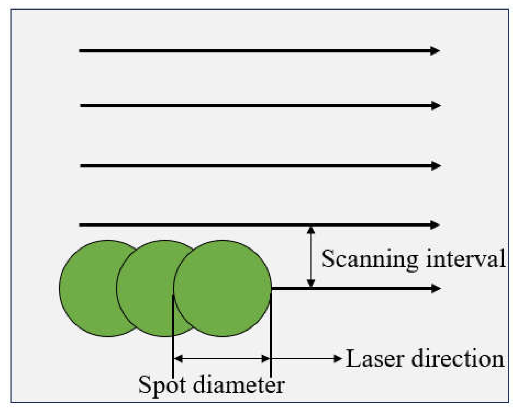
The wavelength of the femtosecond laser used in this study is 515 nm, with a pulse width of 800 fs and a pulse frequency ranging from 1 kHz to 600 kHz. After being emitted from the laser source, the femtosecond laser pulses are focused on the material surface by high-speed scanning mirrors. The diameter of the focused spot is 50μm and its energy distribution approximates a Gaussian distribution. The scanning method for femtosecond laser processing can be referenced from previous work [
13],and a schematic diagram of the laser scanning path is shown in
Figure 1. The samples used in the experiments are sliced N-type 4H-SiC wafers, which are cleaned with ultrasonic waves before being subjected to laser ablation tests. The size of the laser ablation area is 20 mm × 20 mm. After laser processing, the surfaces are chemically-mechanically polished for 30 minutes using nanoparticles of alumina polishing liquid. The surface roughness and morphology of the experimental specimens are measured using a laser confocal microscope.
3. Modeling
When the femtosecond laser interacts with semiconductor materials, the excitation of electrons from the valence band to the conduction band is triggered by a nonlinear absorption process. Since the laser wavelength used in this paper is 515 nm and the energy band width of 4H-SiC is about 3.4 eV, the electrons in the 4H-SiC substrate surface under the action of the femtosecond laser absorb the energy of the two photons for the leptonic transition, and the relaxation time approximation of the Boltzmann equation under the coupled transport equation is used to represent the change in carrier concentration under the action of the femtosecond laser [
14,
15], as shown below:
The first two terms on the right-hand side describe the processes of single-photon absorption and two-photon absorption, respectively. The third term represents the collision ionization process, while the fourth term denotes the Auger recombination process.
Here, is the density of free electrons, is the single-photon absorption coefficient, is the two-photon absorption coefficient, is the collision ionization coefficient, is the Auger recombination coefficient, and is the photon energy. Based on the relationship between the density of free electrons and the material's dielectric constant, transient optical properties such as reflectance and extinction coefficient can be obtained [
16].
Due to the laser incidence on the material surface, when the electron density reaches a certain level, the laser-irradiated region exhibits metallic properties, thereby altering the material's transient optical characteristics. The threshold for the density of free electrons can be calculated as:
where
is the vacuum permittivity,
is the density of transient carriers,
is the electron mass,
is the elementary charge, c is the speed of light in vacuum, and λ is the wavelength of the incident laser. After calculation, under the experimental conditions, the threshold for the density of free electrons is
Based on the one-dimensional two-temperature equation, the temperature changes of electrons and lattice under the action of pulse energies can be analyzed as blow:
where
and
represent the specific heat capacities of electrons and lattice,
and
represent the temperatures of electrons and lattice, and
and
represent the thermal conductivities of electrons and lattice, respectively. In this study, we assume that the initial temperatures of the lattice and electrons are 300 K, corresponding to room temperature air environment, and the initial electron density is 1.0×10
12cm
-3. The standard temperature threshold for ablation is set at the melting point of silicon carbide, i.e., 3003 K. The main parameters of other materials are as follows:
Table 1.
Physical parameters of SiC used in model.
Table 1.
Physical parameters of SiC used in model.
| Parameter |
Symbol |
Unit |
Value [8,17,18,19] |
| Electron-phonon coupling coefficient |
g |
W/(m3•K) |
Ce /τe
|
| Specific heat capacity of electrons |
|
J/(m3•K) |
3 |
| Specific heat capacity of lattice |
|
J/(m3•K) |
1.978×10⁶+3.54×10²-3.68×10⁶ |
| Thermal conductivity of lattice |
|
J/(m•K•s) |
611×102/(-115) |
| energy band width |
Eg
|
eV |
(3.01-6.4×10⁻⁶)/( +1200) |
| single-photon absorption coefficient |
|
1/cm |
50 |
| single-photon absorption coefficient @530nm |
|
m/W |
0.5×10⁻¹¹
|
| Boltzmann constant |
|
J/K |
1.3806505×10⁻²³
|
4. Results and Discussion
4.1. The Numerical Simulation Results
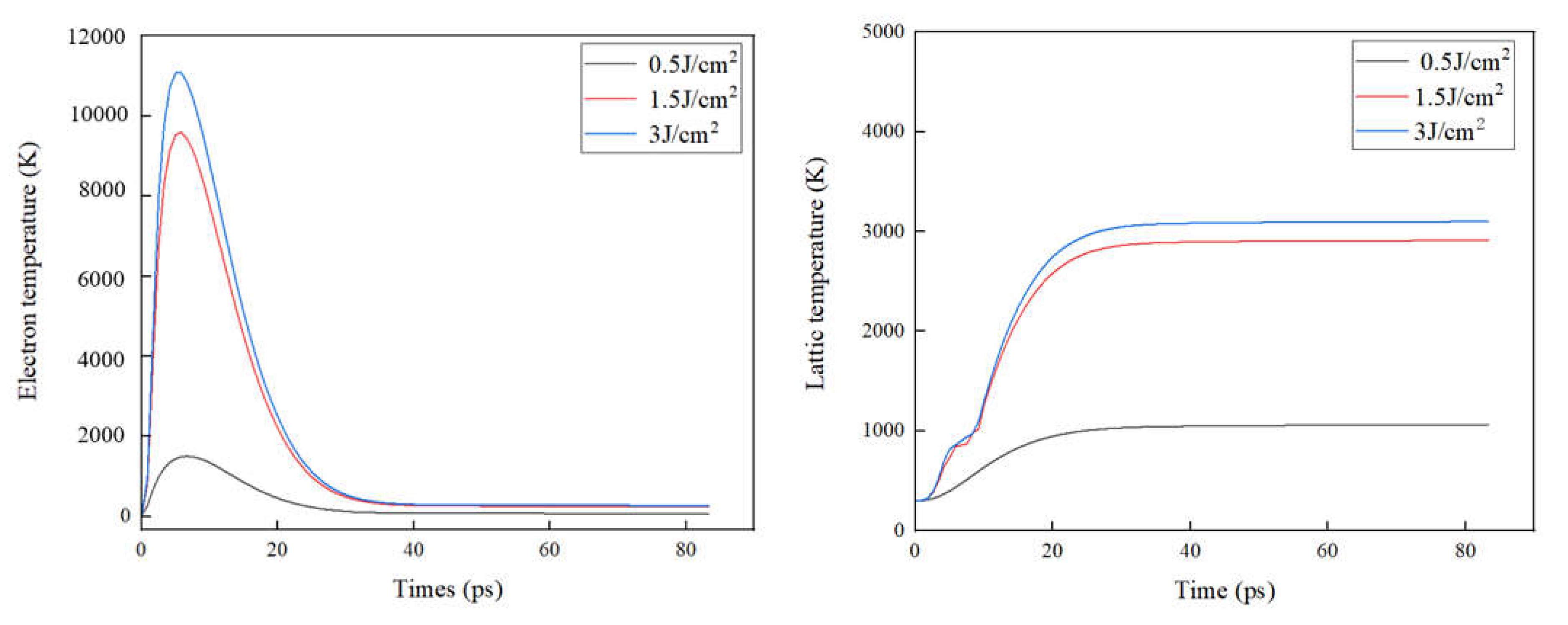
Based on the theoretical model, the laser pulse energy densities are set to 0.5 J/cm², 1.5 J/cm² and 3 J/cm², and the variation of electron and lattice temperatures under single-pulse femtosecond laser irradiation is calculated. It can be seen that the electron temperature increases rapidly under femtosecond laser irradiation, while the lattice temperature increases relatively slowly, as shown in
Figure 2. At a laser energy density of 3 J/cm², the electron temperature can reach a maximum of about 11000 K, followed by a rapid decrease, while the lattice temperature rises to a maximum of 3100 K, the melting temperature of the material, and then continues to diffuse into the lower temperature region. When the laser energy density is 0.5 J/cm², the electron temperature reaches a maximum of about 1800 K, and the maximum lattice temperature is about 1000 K, indicating that the material has not yet undergone ablation. Combining single-pulse and single-pass laser ablation experiments, it is clear that the degree of ablation on the surface of SiC increases with the increase in pulse energy density. Therefore, by adjusting parameters such as laser power and defocus amount to change the laser energy density, different depths of ablation can be achieved, which is consistent with the results of previous experiments in this study.
4.2. Multi-Pass Laser Scanning Experiments
The results of numerical simulations show that the pulse energy density of ultrafast lasers significantly influences the ablation effect. Therefore, multi-pass laser scanning experiments were conducted to analyze the effects of key laser parameters on ablation depth, roughness, and surface morphology. As shown in
Figure 3, the three-dimensional morphology of the ablated surface obtained by laser confocal microscopy shows distinct ripples and grooves under multi-pass laser scanning. The laser energies used were 37.5μJ, 62.5μJ, and 87.5μJ, corresponding to energy densities of 3.7J/cm², 6.2J/cm², and 8.8J/cm², respectively. As the laser energy density increases, the surface ripples become more pronounced, indicating a more significant effect on the surface morphology.
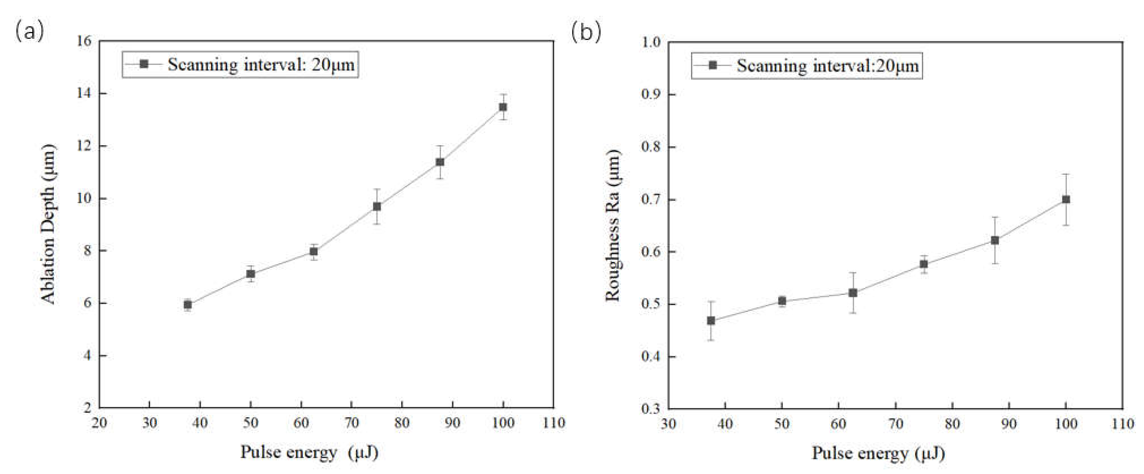
Figure 4 shows the variation of surface depth and roughness with laser energy density with a scanning speed of 500 mm/s, a pulse frequency of 600 kHz and a scanning interval of 20μm. Both ablation depth and surface roughness increase with increasing pulse energy. For example, at a pulse energy of 37.5μJ, the average ablation depth is 5.9μm, while at 87.5μJ, the average surface ablation depth reaches 13.8μm. The initial surface roughness of sliced SiC substrate is 126nm, which increases to an average roughness of 460nm after laser irradiation with a pulse energy of 37.5μJ. At a pulse energy of 87.5μJ, the average surface roughness increases further to 690nm.
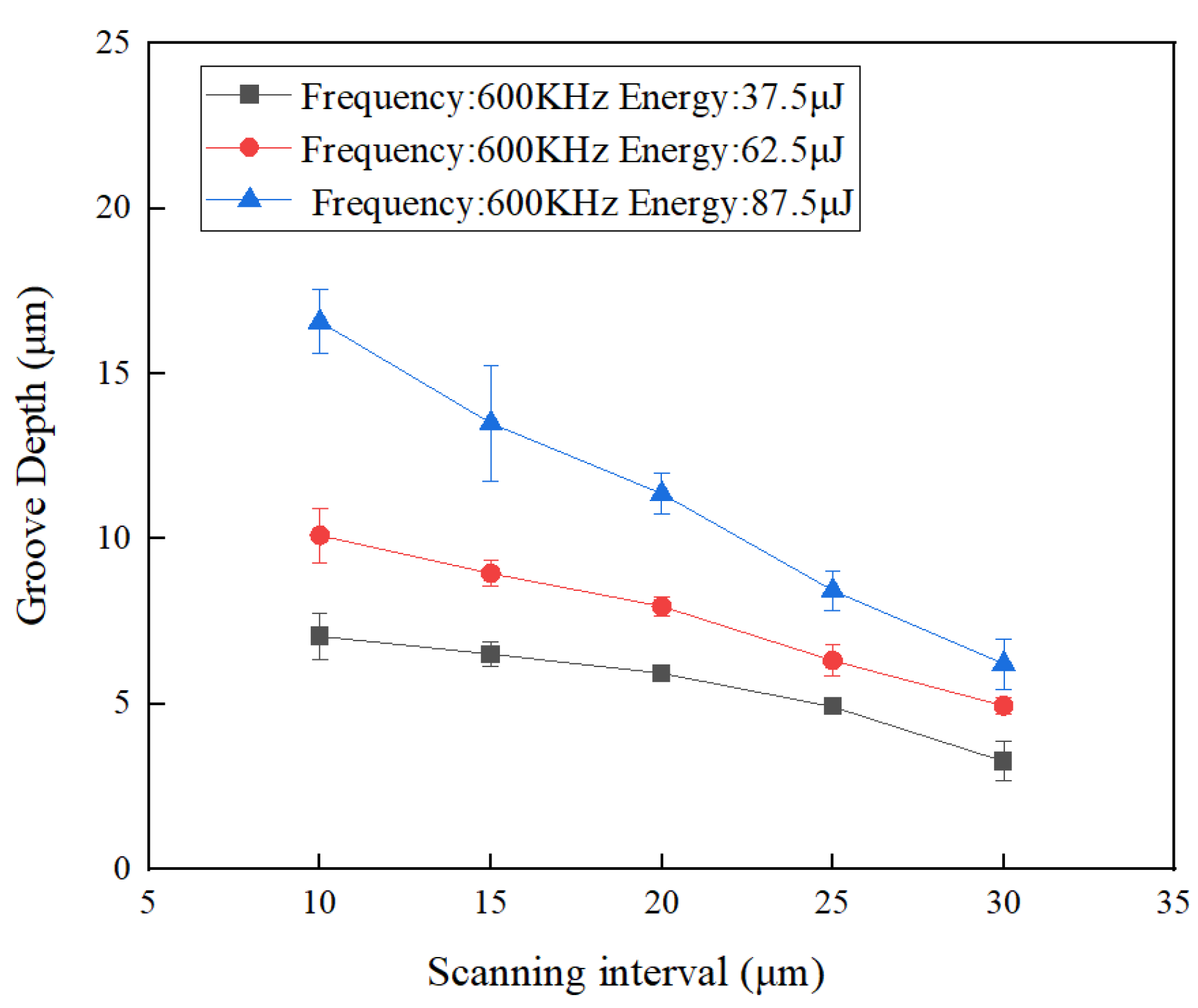
The scanning interval is an important parameter affecting the multi-pass laser scanning ablation. Using a frequency of 600 kHz, a scanning speed of 500 mm/s, and a laser pulse energy of 62.5 µJ, different scanning intervals of 10μm, 15μm, 20μm, 25μm, and 30μm were investigated.
Figure 5 shows the surface images obtained by laser confocal microscopy under different laser energies and scanning intervals. It can be observed that when the scanning interval is 10μm, distinct surface stripes are visible, and the wavy morphology is the most prominent. As the scanning interval increases, the prominence of the stripes gradually decreases. In
Figure 6, the relationship between ablation depth and scanning interval in multi-pass laser scanning ablation is illustrated. It's apparent that the average ablation depth from surface scanning surpasses that from single-pass scanning significantly. By reducing the scanning interval, the laser pulse energy deposited per unit area of the material surface increases, resulting in a corresponding augmentation in ablation depth.
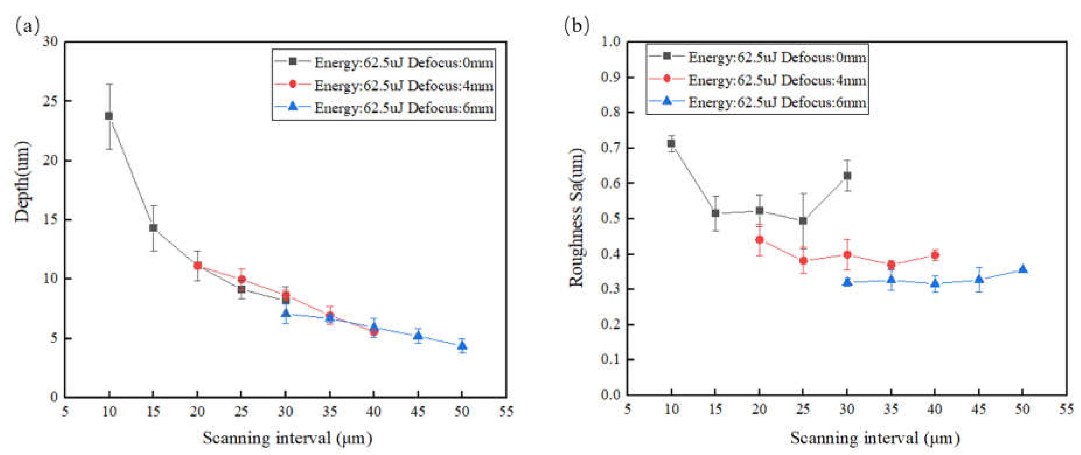
The defocus amount affects the size of the laser beam diameter and the ablation width. As shown in
Figure 7, changes in surface depth and roughness were observed at different defocus settings and changing the scanning interval. As the defocus amount increases, the ablation depth decreases significantly. This phenomenon is mainly due to the decrease in energy density when the laser beam is out of focus, resulting in a reduction in the ablation depth. Conversely, increasing the defocus amount can lead to a reduction in surface roughness.
Based on the results of multi-pass laser scanning, parameters such as laser pulse energy, scanning interval, and defocus amount have different effects on ablation depth, surface roughness, and surface morphology. By comparing the ablation depth and roughness, it can be observed that deeper ablation results in higher surface roughness. Therefore, to achieve lower surface roughness, it is necessary to reduce the amount of material removed. Laser ablation treatment effectively removes defects from the surface of sliced SiC wafers, but it generally increases the surface roughness. Therefore, further polishing is required to achieve an optimized surface quality.
4.3. Surface Polishing of Ablated SiC Substrate
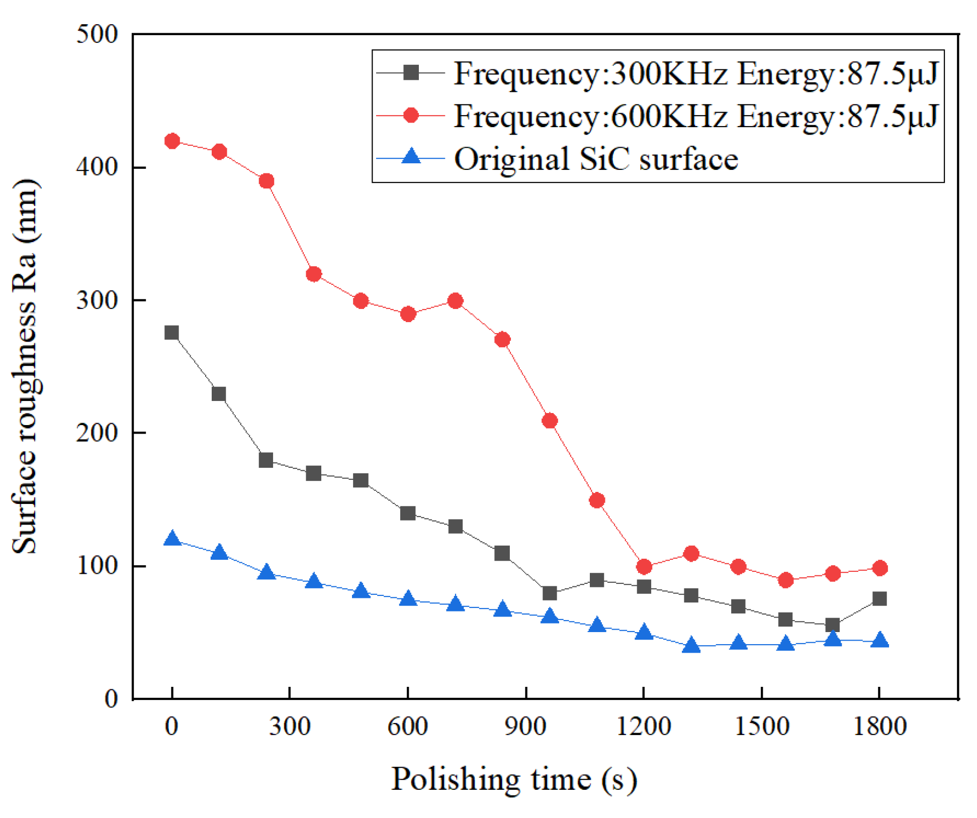
The surface polishing of sliced SiC samples after laser ablation is described in this section. The laser processing parameters were as follows: laser energy of 87.5μJ, scanning interval of 30μm, scanning speed of 500 mm/s, defocus amount of +6mm, and pulse frequencies of 300 kHz and 600 kHz, respectively, and the ablated surface roughness (Ra) was measured to be 276 nm and 420 nm. Surface polishing was performed using alumina polishing liquid. During the polishing process, the surface roughness of the material was measured every 2 minutes to obtain efficiency information on material removal, as shown in
Figure 8. The ablated samples showed a darkened surface color due to the laser ablation. As polishing progressed, the surface tended to become smooth and transparent. In the early stages of polishing, there was a rapid decrease in surface roughness, primarily due to the rapid removal of abrasive interactions with surface protrusions. In addition, material removed during polishing accumulated in the pits, reducing roughness. As the polishing approached the silicon carbide single crystal layer, the polishing efficiency decreased and the decrease in surface roughness became less pronounced. The removal of pits caused by uneven laser energy distribution was challenging, requiring ablation thicknesses of 15 to 20 μm to achieve a flat surface structure. After 30 minutes of surface polishing, the surface roughness of the ablated samples was reduced to approximately 85 nm. Further polishing could achieve even lower surface roughness.
5. Conclusions
Based on the two-temperature model, we elaborated the femtosecond laser surface ablation process of sliced SiC substrate. The results show that when the femtosecond laser interacts with silicon carbide crystals, the electron temperature and electron density on the material surface rapidly increase, while the lattice temperature slowly increases to the melting point. In addition, the degree of ablation increases as the pulse energy density increases. The influence of femtosecond laser parameters on surface roughness and ablation depth was further analyzed through multi-pass laser scanning experiments. The results indicate that parameters such as laser pulse energy, scanning interval, and defocus amount all have effects on ablation depth, surface roughness, and surface morphology. There is a positive correlation between ablation depth and surface roughness, with greater ablation depth corresponding to greater surface roughness. The polishing treatment on the ablated surfaces and found that the surface roughness decreased rapidly. After 30 minutes of polishing, the surface roughness decreased to approximately 85 nanometers. This suggests that femtosecond laser surface ablation followed by polishing treatment can achieve improved surface quality.
Author Contributions
Data Curation, Ziqiang Zhao; Writing – Original Draft Preparation, Ziqiang Zhao; Writing – Review & Editing, Lin Zhao; Supervision, Yun Peng.
Acknowledgments
This research did not receive any specific grant from public, commercial, or nonprofit funding agencies. We thank the High-Power and Ultrafast Laser Manufacturing Lab for providing the necessary equipment for this study, and we thank Professor. Huang Ting and Ms. Xing Lingrong for their technical assistance during the experiment.
Conflicts of Interest
The authors declare that they have NO affiliations with or involvement in any organization or entity with any financial interest in the subject matter or materials discussed in this manuscript. This research received no external funding.
References
- Kato, T. et al., “High throughput SiC wafer polishing with good surface morphology,” in Materials Science Forum, Trans Tech Publications Ltd, 2007, pp. 753–756. [CrossRef]
- Hardin, C.W.; Qu, J.; Shih, A.J. , “Fixed Abrasive Diamond Wire Saw Slicing of Single-Crystal Silicon Carbide Wafers,” Materials and Manufacturing Processes, vol. 19, no. 2, pp. 355–367, Dec. 2004. [CrossRef]
- Inasaki, I. , “Grinding of Hard and Brittle Materials,” CIRP Annals, vol. 36, no. 2, pp. 463–471, 1987. [CrossRef]
- Zheng, Q. et al., “Investigation on the underwater femtosecond laser polishing SiC ceramic,” Ferroelectrics, vol. 564, no. 1, pp. 28–36, Aug. 2020. [CrossRef]
- Shao, Y. et al., “Laser-assisted thermochemical ultrahigh-precision polishing of titanium in phosphoric acid solution,” The International Journal of Advanced Manufacturing Technology, vol. 115, no. 4, pp. 1201–1210, Jul. 2021. [CrossRef]
- Taylor, L.L.; Qiao, J.; Qiao, J. , “Femtosecond laser polishing of optical materials,” J. L. Bentley and S. Stoebenau, Eds., Oct. 2015, p. 96330M. [CrossRef]
- Taylor, L.L.; Xu, J.; Pomerantz, M.; Smith, T.R.; Lambropoulos, J.C.; Qiao, J. , “Femtosecond laser polishing of germanium [Invited],” Opt Mater Express, vol. 9, no. 11, p. 4165, Nov. 2019. [CrossRef]
- Tsibidis, G.D.; Mouchliadis, L.; Pedio, M.; Stratakis, E. , “Modeling ultrafast out-of-equilibrium carrier dynamics and relaxation processes upon irradiation of hexagonal silicon carbide with femtosecond laser pulses,” Phys Rev B, vol. 101, no. 7, p. 075207, Feb. 2020. [CrossRef]
- Rehman, Z.U.; Janulewicz, K.A. , “Structural transformations in femtosecond laser-processed n-type 4H-SiC,” Appl Surf Sci, vol. 385, pp. 1–8, Nov. 2016. [CrossRef]
- Feng, S.; Zhang, R.; Huang, C.; Wang, J.; Jia, Z.; Wang, J. , “An investigation of recast behavior in laser ablation of 4H-silicon carbide wafer,” Mater Sci Semicond Process, vol. 105, p. 104701, Jan. 2020. [CrossRef]
- Wang, L.; Zhao, Y.; Yang, Y.; Zhang, M.; Zhao, Y. , “Experimental Investigation on Ablation of 4H-SiC by Infrared Femtosecond Laser,” Micromachines (Basel), vol. 13, no. 8, p. 1291, Aug. 2022. [CrossRef]
- Zhang, R.; Huang, C.; Wang, J.; Zhu, H.; Yao, P.; Feng, S. , “Micromachining of 4H-SiC using femtosecond laser,” Ceram Int, vol. 44, no. 15, pp. 17775–17783, Oct. 2018. [CrossRef]
- Zhao, Z.; Zhao, L.; Peng, Y. , “Experimental study on femtosecond laser ablation of 4H–SiC substrate,” Journal of Micromechanics and Microengineering, vol. 34, no. 2, p. 025005, Feb. 2024. [CrossRef]
- Papadopoulos, A.; Skoulas, E.; Tsibidis, G.D.; Stratakis, E. , “Formation of periodic surface structures on dielectrics after irradiation with laser beams of spatially variant polarisation: a comparative study,” Applied Physics A, vol. 124, no. 2, p. 146, Feb. 2018. [CrossRef]
- Rethfeld, B.; Ivanov, D.S.; Garcia, M.E.; Anisimov, S.I. , “Modelling ultrafast laser ablation,” J Phys D Appl Phys, vol. 50, no. 19, p. 193001, May 2017. [CrossRef]
- Jiang, L.; Wang, A.-D.; Li, B.; Cui, T.-H.; Lu, Y.-F. , “Electrons dynamics control by shaping femtosecond laser pulses in micro/nanofabrication: modeling, method, measurement and application,” Light Sci Appl, vol. 7, no. 2, pp. 17134–17134, Aug. 2017. [CrossRef]
- Galeckas, A.; Linnros, J.; Grivickas, V.; Lindefelt, U.; Hallin, C. , “Auger recombination in 4H-SiC: Unusual temperature behavior,” Appl Phys Lett, vol. 71, no. 22, pp. 3269–3271, Dec. 1997. [CrossRef]
- Nilsson, O. et al., “Determination of the thermal diffusivity and conductivity of monocrystalline silicon carbide (300-2300 K),” High Temperatures-High Pressures, vol. 29, no. 1, pp. 73–79, 1997. [CrossRef]
- Guo, X. et al., “Nonlinear optical properties of 6H-SiC and 4H-SiC in an extensive spectral range,” Opt Mater Express, vol. 11, no. 4, p. 1080, Apr. 2021. [CrossRef]
|
Disclaimer/Publisher’s Note: The statements, opinions and data contained in all publications are solely those of the individual author(s) and contributor(s) and not of MDPI and/or the editor(s). MDPI and/or the editor(s) disclaim responsibility for any injury to people or property resulting from any ideas, methods, instructions or products referred to in the content. |
© 2024 by the authors. Licensee MDPI, Basel, Switzerland. This article is an open access article distributed under the terms and conditions of the Creative Commons Attribution (CC BY) license (http://creativecommons.org/licenses/by/4.0/).
