Submitted:
29 May 2024
Posted:
30 May 2024
You are already at the latest version
Abstract
We experimentally demonstrate waveguide and microring resonator (MRR) polarizers by integrating 2D graphene oxide (GO) films onto silicon (Si) photonic devices. The 2D GO films with highly anisotropic light absorption are on-chip integrated with precise control over their thicknesses and sizes. Detailed measurements are performed for the fabricated devices with different GO film thicknesses, coating lengths, and Si waveguide widths. The results show that a maximum polarization-dependent loss (PDL) of ~17 dB is achieved for the hybrid waveguides, and the hybrid MRRs achieved a maximum polarization extinction ratio (PER) of ~10 dB. We also characterize the wavelength- and power-dependent response for these polarizers. The former demonstrates a broad operation bandwidth of over ~100 nm, and the latter verifies performance improvement enabled by photo-thermal changes in GO films. By fitting the experimental results with theoretical simulations, we find that the anisotropy in the loss of GO films dominates the polarization selectivity of these devices. These results highlight the strong potential of 2D GO films for realizing high-performance polarization selective devices in Si photonic platform.
Keywords:
graphene oxide
; polarizers
; silicon
; nanophotonics
Optical polarizers transmit light only polarised in one direction while blocking perpendicularly polarized light. They are important functions for modern optical systems.[1,2] They have facilitated polarization selection and control in a wide range of applications, such as optical sensing,[3,4] imaging and display,[5,6] optical analysis,[7,8] and optical communications.[9,10]
A variety of optical polarizers have been implemented based on different bulk material device platforms, such as refractive prisms,[11,12] birefringent crystals,[13,14] fiber components,[15,16] and integrated photonic devices.[17,18] Amongst these, integrated photonic polarizers, particularly those based on the well-developed silicon (Si) photonic platform, offer attractive advantages of compact footprint, low power consumption, and the capability for large-scale manufacturing. Nevertheless, the rapid advancement of photonics industries drives the demand for high-performance optical polarizers across broad wavelength ranges, which is usually challenging for optical polarizers based on bulk materials.[19,20,21]
Recently, owing to their high anisotropy in light absorption and broadband response, 2D materials, such as graphene,[22,23] graphene oxide (GO),[24,25] transition-metal dichalcogenides (TMDCs),[26,27] and black phosphorus,[28] have been on-chip integrated to realize optical polarizers with high performance and new features. As a common derivative of graphene, GO with facile fabrication processes for precise on-chip integration shows a high compatibility with integrated device platforms.[29,30,31] Previously, we reported high performance waveguide and microring resonator (MRR) polarizers by integrating 2D GO films onto high index doped silica devices.[25] In this work, we further integrate 2D GO films onto the more widely used Si photonic devices to realize waveguide and MRR polarizers. Precise control of the GO film thicknesses is achieved by using a transfer-free and layer-by-layer film coating method, together with window opening on the upper cladding of Si photonic devices to control the film coating lengths. We perform detailed measurements for the fabricated devices with different GO film thicknesses, coating lengths, and Si waveguide widths, achieving a maximum polarization-dependent loss (PDL) of ~17 dB for the waveguide polarizers and a maximum polarization extinction ratio (PER) for the MRR polarizers. The wavelength- and power-dependent response of these polarizers is also characterized, showing a broad operation bandwidth over ~100 nm and improvement in the polarization selectivity enabled by photo-thermal changes in GO films. Finally, we perform theoretical analysis by fitting the experimental results with theory, which reveals that the anisotropy in the loss of GO films dominates the polarization selectivity of these polarizers. These results verify the effectiveness of integrating 2D GO films onto Si photonic devices for implementing high-performance optical polarizers.
Figure 1a illustrates the atomic structure of monolayer GO, in which the carbon network is decorated with diverse oxygen functional groups (OFGs) such as epoxide, hydroxyl, and carboxylic groups.[32,33] Unlike graphene that has a zero bandgap and exhibits metallic behavior,[34] GO is a dielectric material with an opened bandgap typically ranging between ~2.1 and ~3.6 eV.[30,32] This bandgap is larger than the energy of two photons at 1550 nm (i.e., ~1.6 eV), which yields both low linear light absorption and two-photon absorption (TPA) in the telecom band.
Figure 1.
(a) Schematic of GO’s atomic structure. (b) Schematic illustration of a waveguide optical polarizer based on a Si waveguide integrated with a monolayer GO film. Inset illustrates the layered structure of GO films fabricated by the self-assembly method. (c) TE and TM mode profiles for the hybrid waveguide in (b). (d) Microscopic image of the fabricated devices on a silicon-on-insulator (SOI) chip coated with a monolayer GO film. (e) Measured Raman spectra of the SOI chip in (d) before and after coating the GO film.
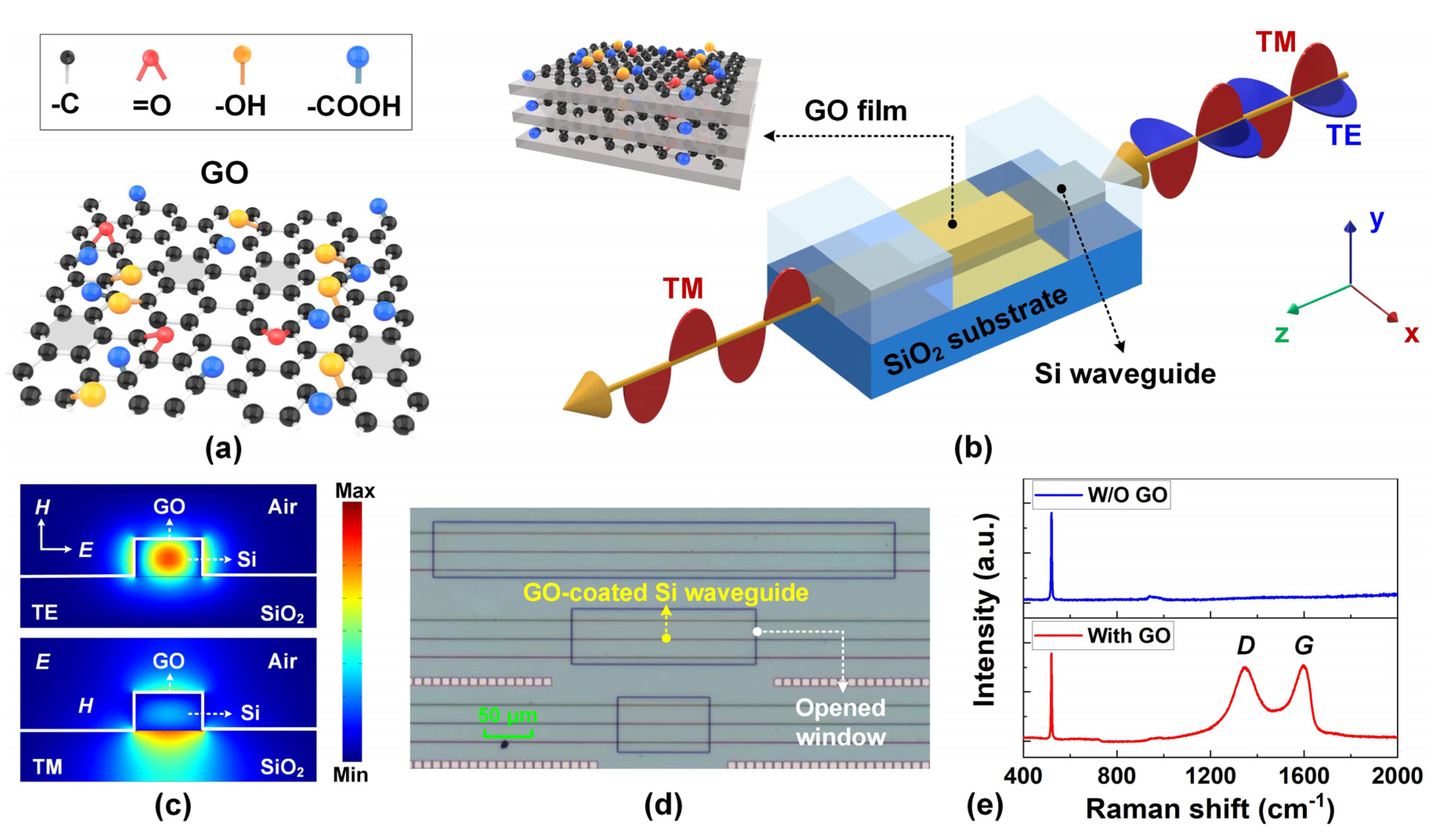
Figure 1b shows the schematic of a Si nanowire waveguide integrated with a monolayer GO film. The corresponding transverse electric (TE) and transverse magnetic (TM) mode profiles for the hybrid waveguide are shown in Figure 1c, which were simulated using a commercial mode solving software (COMSOL Multiphysics). The width and height of the Si waveguide are 400 nm and 220 nm, respectively. Due to the interaction between the evanescent field from the Si waveguide and the 2D GO film with strong anisotropy in its light absorption, the hybrid waveguide exhibits much stronger light absorption for TE (in-plane) polarization than TM (out-of-plane) polarization. This enables it to function as a TM-pass optical polarizer.
Figure 1d shows a microscopic image of the fabricated devices on a silicon-on-insulator (SOI) chip. The device layout was patterned via 248-nm deep ultraviolet lithography followed by inductively coupled plasma etching. A silica upper cladding was deposited onto the fabricated Si waveguides. To enable light-GO interaction, lithography and dry etching processes were employed to open windows on the silica upper cladding to allow the coating of GO films onto the Si waveguides. We fabricated devices with 5 different lengths (ranging between ~0.1 mm and ~2.2 mm) for the opened windows, which correspond to different GO film coating lengths in the hybrid waveguides. The GO films were coated layer-by-layer and transfer-free with a solution-based self-assembly process.[25,31] This coating process has significant advantages over commonly used mechanical transfer methods for coating 2D materials,[35,36] achieving large-area conformal coating onto nanostructures, precise film thickness control, and high film uniformity.[29,30] As shown in Figure 1d, the good morphology of the coated GO films provides evidence for the high film uniformity achieved by our coating method.
Figure 1e shows the measured Raman spectra of the SOI chip in Figure 1d before and after coating a monolayer GO film. The GO film had a thickness of ~2 nm, which was characterized by atomic force microscopy measurement. In the Raman spectrum for the GO-coated chip, the presence of the representative D (1345 cm−1) and G (1590 cm−1) peaks verifies the successful on-chip integration of the GO film.
In Figure 2, we show the results for the measured insertion losses (IL’s) of the fabricated devices for input light with different polarization states. We measured devices with different GO layer numbers (N), GO coating lengths (LGO), and Si waveguide widths (W). For all the devices, the total length of the Si waveguides was ~3.0 mm. In our measurements, a continuous-wave (CW) light at ~1550 nm was butt coupled into / out of the devices via lensed fibers. The fiber-to-chip coupling loss was ~5 dB per facet. For comparison, the input power was kept the same as Pin = ~0 dBm. Unless otherwise specified, the values of Pin and IL in our discussion refer to those after excluding the fiber-to-chip coupling loss.
Figure 2.
(a) Measured (i) TE- and (ii) TM-polarized insertion loss (IL) versus GO coating length LGO for the hybrid waveguides with 1−5 layers of GO. (iii) shows the polarization dependent loss (PDL) calculated from (i) and (iii). (b) Measured (i) TE-, (ii) TM- polarized IL versus Si waveguide width W for the hybrid waveguides with 1−5 layers of GO. (iii) shows the PDL calculated from (i) and (iii). (c) Polar diagrams for the measured IL of devices with different GO layer numbers of (i) N = 1, (ii) N = 3, and (iii) N = 5. The polar angle represents the angle between the input polarization plane and the substrate. In (a) ‒ (c), the input CW power and wavelength were ~0 dBm and ~1550 nm, respectively. In (a) and (b), the data points depict the average of measurements on three duplicate devices and the error bars illustrate the variations among the different devices. In (a), W = ~400 nm. In (b), LGO = ~2.2 mm. In (c), LGO = ~2.2 mm and W = ~400 nm.
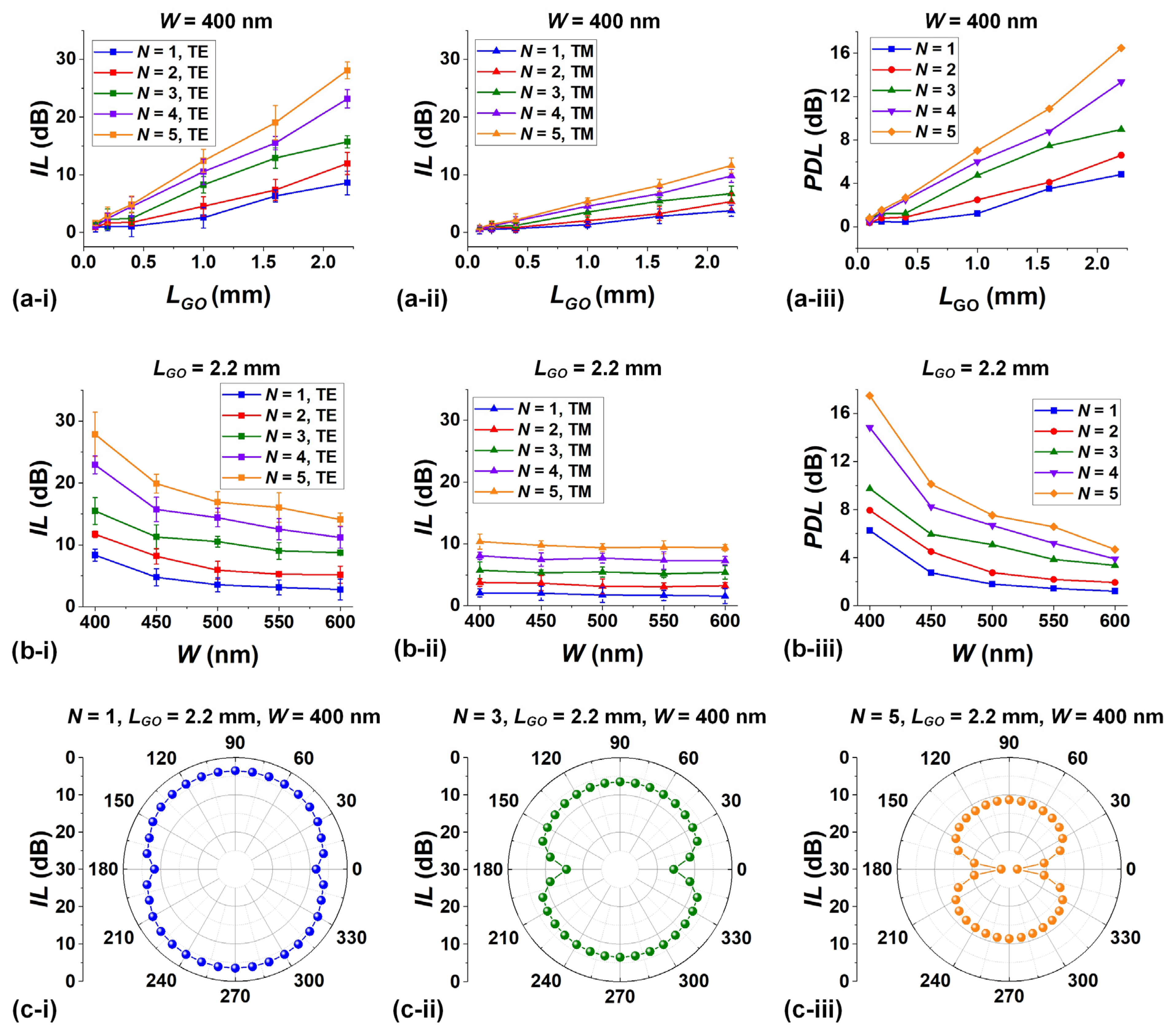
Figure 2(a-i),(a-ii) show the measured IL versus GO coating length LGO for TE- and TM-polarized input light, respectively. Here we show the results for the hybrid waveguides with 1 ‒ 5 layers of GO (i.e., N = 1 ‒ 5). For comparison, all the uncoated Si waveguides had the same waveguide width of W = ~400 nm. In our measurements, three duplicate devices were measured, and the data points depict their average values, with the error bars illustrating the variations for different samples. It can be seen that the IL increases with LGO and N for both polarizations, with the TE polarization showing a more significant increase than the TM polarization. In Figure 2(a-iii), we further calculated the PDL (dB) by subtracting the TM-polarized IL (dB) from the TE-polarized IL (dB). As can be seen, the PDL increases with LGO and N. For the 5-layer device with LGO = ~2.2 mm, a maximum PDL value of ~17 dB was achieved. In contrast, the uncoated Si waveguide did not show any significant polarization dependent IL, with the PDL being less than 0.2 dB. The difference in the TM-polarized IL values between the uncoated and hybrid waveguides reflects the minimum excess insertion loss induced by the GO film. For the 5-layer device with LGO = ~2.2 mm, the difference was ~10 dB.
Figure 2(b-i),(b-ii) show the measured IL versus W for TE- and TM-polarized input light, respectively. Here, all the hybrid waveguides had the same LGO = ~2.2 mm. For both polarizations, the IL increases with GO layer number N. In contrast to the results in Figure 2(a-i),(a-ii), the IL decreases as W increases, with the TE polarization showing a more significant decrease than the TM polarization. This results in the decrease of PDL for an increasing W in Figure 2(b-iii). For the 5-layer device with W = ~600 nm, the PDL was ~5 dB, which was ~12 dB lower than that of the comparable device with W = ~400 nm.
Figure 2c shows the polar diagrams for the measured IL of devices with different GO layer numbers (i.e., N = 1, 3, and 5). Except for the GO layer number, the other device parameters were kept the same (i.e., W = ~400 nm and LGO = ~2.2 mm). In the polar diagrams, the variations in the IL values across various polarization angles further confirm the polarization selection capability for the hybrid waveguides. Compared to the 5-layer device that achieved a PDL of ~17 dB, the 1-layer and 3-layer devices achieved lower PDL values of ~5 dB and ~9 dB, respectively.
Figure 3a shows the measured PDL versus wavelength of the input CW light. In Figure 3(a-i), we show the results for the hybrid waveguides with 1 ‒ 5 layers of GO (i.e., N = 1 ‒ 5) and all of them had the same LGO = ~2.2 mm and W = ~400 nm. In Figure 3(a-ii), we show the results for the hybrid waveguides with different LGO but the same N = 5 and W = ~400 nm. For all the devices in Figure 3a, the PDL shows a very small variation that was less than 1 dB within the measured wavelength range of ~1500 ‒ 1600 nm. This reflects the broad operation bandwidth for these waveguide polarizers. We note that there was a slight increase in the PDL as the wavelength increased, which can be attributed to a minor change in GO’s mode overlap induced by dispersion. In our measurements, the wavelength tuning range was limited by the employed tunable CW laser. The light absorption bandwidth for GO is in fact quite broad, which covers infrared wavelengths and extends into the visible and terahertz (THz) ranges.[29,37] Such broadband response enables a much broader operation bandwidth (potentially spanning several hundreds of nanometers, as we demonstrated in Ref. [25]) than that demonstrated here. This represents a significant advantage of 2D-material-based polarizers, which is usually challenging to achieve for integrated photonic devices based on only bulk materials.[2,38]
Figure 3.
(a) Measured PDL versus wavelength of input CW light for (i) devices with different GO layer numbers (N) but the same GO coating length (LGO) of ~2.2 mm and (ii) devices with different LGO but the same N = 5. (b) (i) Measured TE and TM polarized IL versus input power (Pin) for devices with different N = 1, 3, and 5 but the same LGO = ~2.2 mm. (ii) shows the PDL calculated from (i). (c) (i) Measured TE and TM polarized IL versus Pin for devices with different LGO = 0.2, 1.0, and 2.2 mm but the same N = 5. (ii) shows the PDL calculated from (i). In (a)–(c), W = ~400 nm. In (a), Pin = ~0 dBm. In (b) and (c), the input CW wavelength was ~1550 nm.
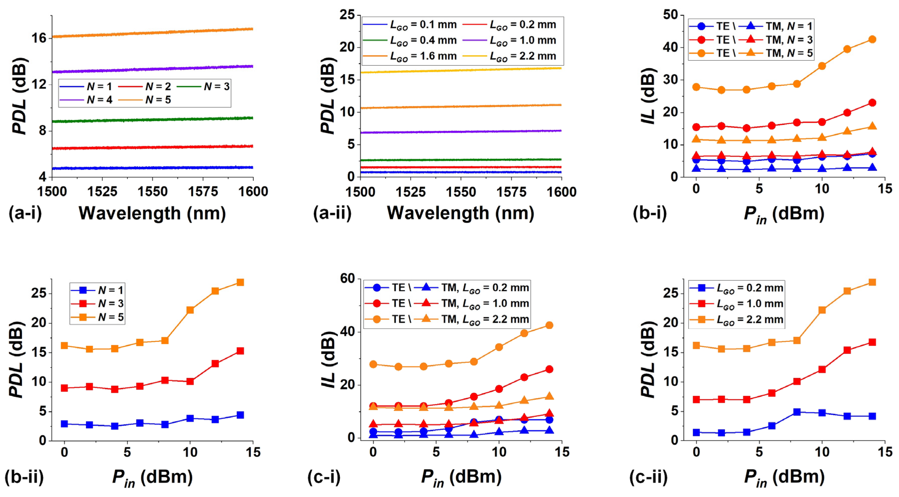
Figure 3(b-i) shows the measured IL versus input power Pin for the hybrid waveguides with 1, 3, and 5 layers of GO. Here all the devices had the same LGO = ~2.2 mm and W = ~400 nm. As Pin increases, the IL increases for both polarizations, with the TE polarization showing a more significant increase than the TM polarization. The increased IL was induced by the photo-thermal reduction of GO at high light powers, where reduced GO exhibited stronger light absorption than unreduced GO.[30,39] Another interesting feature for the reduction of GO induced by photo-thermal effects is its reversibility within a certain power range.[39,40] This originates from the instability of photo-thermally reduced GO, which can readily return to the unreduced state after cooling in oxygen containing atmosphere (e.g., after tuning off the optical input). Since the hybrid waveguides exhibited stronger absorption for TE-polarized light, the reduction of GO occurred more readily for TE polarization, resulting in a more significant change in the corresponding IL in Figure 3(b-i). We also note that the 5-layer device showed more significant changes in the IL as compared to the 3-layer and 1-layer devices, which reflects the fact that there were more significant photo-thermal effects in thicker GO films. In Figure 3(b-ii), we show the calculated PDL versus Pin, where the PDL increases for an increasing Pin. This indicates that the polarization selectivity was further improved by increasing the input power. At Pin = ~15 dBm, the PDL for the 5-layer device was ~25 dB, representing an ~8-dB improvement relative to the PDL at Pin = ~0 dBm.
Figure 3(c-i) shows the measured IL versus Pin for the hybrid waveguides with three different LGO but the same N = 5 and W = ~400 nm. The extracted PDL versus Pin is shown in Figure 3(c-ii). For all the devices, the PDL starts to increase at almost the same power threshold of Pin = ~6 dB. After that, the devices with LGO = ~1.0 mm and ~2.2 mm exhibit a similar rate of increase, whereas the rate for the device with LGO = ~0.2 mm gradually decreases. This reflects an interesting fact that the reduction of GO induced by the photo-thermal effects was non-uniform along the waveguide. It first occurred at the start of the GO section near the input port and became weaker in tandem with the attenuation of the light power along the waveguide.
Based on the results in Figure 2 and Figure 3, we further analyze the properties of 2D GO films by fitting the experimental results with theoretical simulations. Figure 4(a-i) shows the propagation losses (PL’s) of the hybrid waveguides versus GO layer number N for both polarizations, which were extracted from the measured IL’s in Figure 2(a-i),(a-ii). Figure 4(a-ii) shows the extinction coefficients (k’s) of 2D GO films obtained by fitting the PL’s in Figure 4(a-i) with optical mode simulations, and the ratios of TE- to TM-polarized k values are further plotted in Figure 4(a-iii). For all different N, the GO films exhibit much larger k values for TE polarization than TM polarization in Figure 4(a-ii), highlighting the high anisotropy in their light absorption. For both polarizations, there is a slight increase in k as N increases. This can possibly be attributed to more significant scattering loss in thicker GO films, which can be induced by increased film unevenness and imperfect contact between adjacent layers. It is also interesting to note that in Figure 4(a-iii) the ratio of the k values remains relatively consistent without any significant variations.
Figure 4.
(a-i) TE- and TM-polarized waveguide propagation loss (PL) versus GO layer number (N) for the hybrid waveguides with 1−5 layers of GO. (a-ii) Extinction coefficients (k’s) of 2D GO films obtained by fitting the results in (a-i) with optical mode simulations. (a-iii) Ratios of k values for TE and TM polarizations (kTE / kTM) extracted from (a-ii). (b) Measured (Exp.) and simulated (Sim.) PDL versus Si waveguide width (W) for the hybrid waveguides with 5 layers of GO. The simulated PDL values were obtained by using the same k value for both TE and TM polarizations. (c-i) Measured (Exp.) and simulated (Sim.) PDL versus N. (c-ii) Fractional contributions (η’s) to the overall PDL from polarization-dependent mode overlap and material loss anisotropy, which were extracted from (c-i). (d-i) TE- and TM-polarized PL versus input power (Pin) for the hybrid waveguide with 5 layers of GO. (d-ii) k’s of 2D GO films obtained by fitting the results in (d-i) with optical mode simulations. (d-iii) kTE / kTM extracted from (d-ii). In (a) ‒ (d), the GO coating length LGO = ~2.2 mm. In (a) ‒ (c), Pin = ~0 dBm. In (a), (c), and (d), W = ~400 nm.
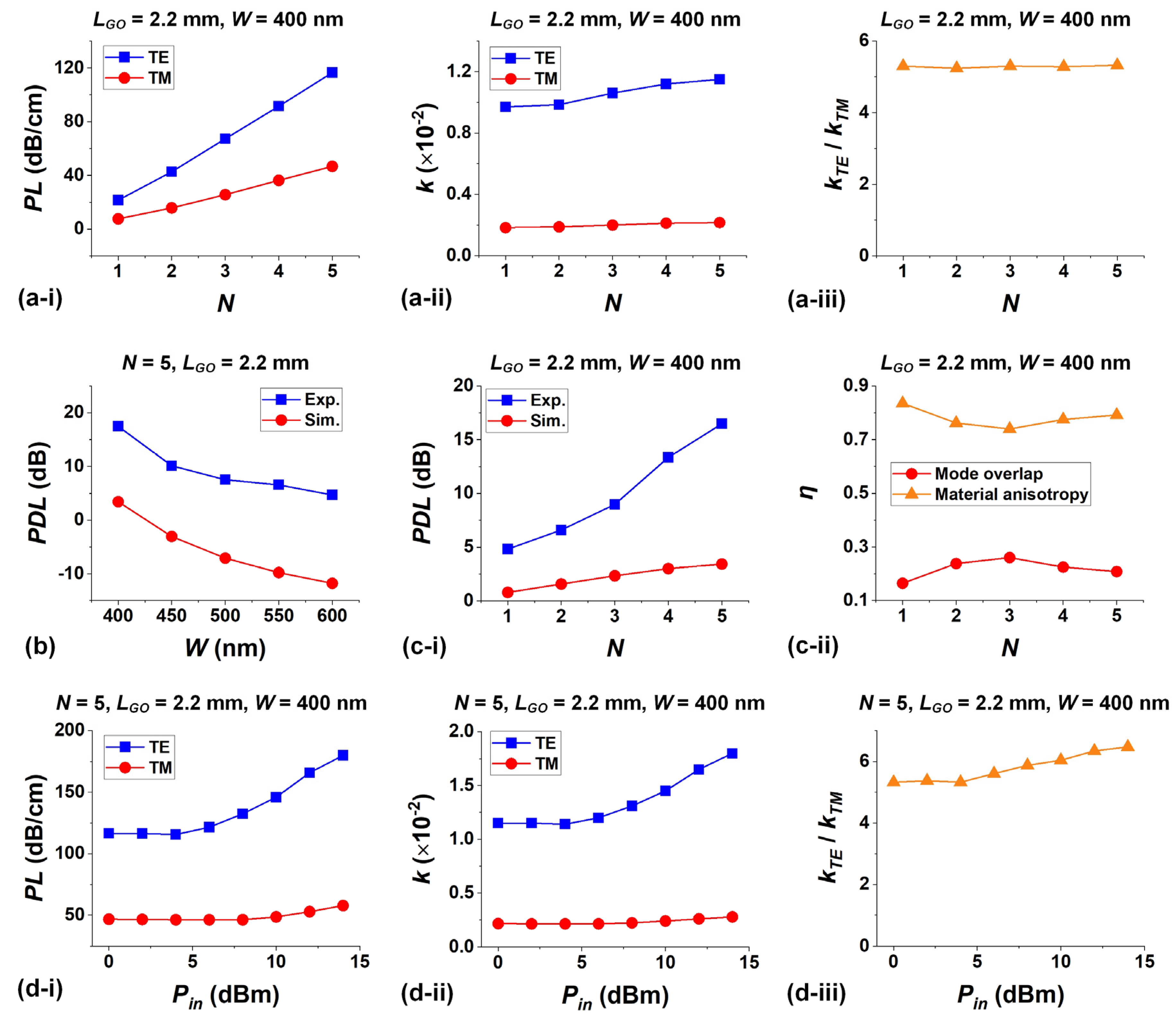
In Figure 4b, we compare the measured PDL values with those obtained from optical mode simulations. In our simulations, we assumed that the GO films were isotropic with the same k value (i.e., kTE for N = 5 in Figure 4(a-ii)) for both TE and TM polarizations. As a result, the simulated PDL values represent the polarization selectivity enabled by the polarization-dependent GO mode overlap, and the difference between the measured and simulated PDL values reflects the extra polarization selectivity provided by the loss anisotropy of GO films. The simulated PDL values are negative when W > 400 nm. This is because the polarization-dependent GO mode overlap induces a higher loss for TM polarization. Despite this, the net PDL values remain positive, indicating that the material loss anisotropy compensates for the negative PDL induced by GO mode overlap.
Similar to that in Figure 4b, in Figure 4(c-i) we show the measured and simulated PDL values for the devices with different N but the same W = ~400 nm. Unlike that in Figure 4b, both the measured and simulated PDL’s show positive values for all different N. This suggests that the polarization-dependent GO mode overlap also contributes to the overall PDL. In Figure 4(c-ii), we further calculated the fractional contributions to the overall PDL from the polarization-dependent mode overlap and the material loss anisotropy (where the sum of the two fractions equals to 1). As can be seen, the contribution from the material loss anisotropy, which accounts for more than 70% for all different GO layer numbers, dominates the overall PDL. This further highlights the significance of the anisotropic 2D GO films in facilitating the functionality of the polarizer.
Figure 4(d-i) shows the PL’s of the hybrid waveguides versus input CW power Pin for both polarizations, which were extracted from the measured IL’s in Figure 3b. Figure 4(d-ii) shows the k values of 2D GO films obtained by fitting the PL’s in Figure 4(d-i) with optical mode simulations, and Figure 4(d-iii) shows the ratios of the TE- to TM-polarized k values in Figure 4(d-ii). In Figure 4(d-ii), k increases with Pin for both polarizations, with the TE polarization showing a more significant increase than the TM polarization. In Figure 4(d-iii), the ratio between the k values slightly increases with Pin, which is also resulting from the more significant photo-thermal effects in GO films induced by stronger absorption of TE-polarized light.
Except for waveguide optical polarizers, we also integrated 2D GO films onto Si MRRs to implement polarization-selective MRRs. Figure 5a shows the device schematic, and Figure 5b shows a microscopic image of the fabricated device with a monolayer GO film. The MRRs were fabricated together with the waveguides in Figure 1d via the same processes. The rings and the bus waveguides had the same width of W = ~400 nm. The radius of the MRRs was ~20 μm, and the length of the opened windows on the MRRs was ~10 μm.
Figure 5.
(a) Schematic illustration of a GO-coated Si microring resonator (MRR) as a polarization-selective MRR. (b) Microscopic image of a fabricated Si MRR coated with a monolayer GO film. (c) Measured (i) TE- and (ii) TM-polarized transmission spectra of the hybrid MRRs with 1 and 2 layers of GO (N = 1, 2). The corresponding results for the uncoated MRR (N = 0) are also shown for comparison. (d) Extinction ratios (ER’s) for the MRRs extracted from (c). (e) Polarization extinction ratios (PER’s) extracted from (d). In (c) ‒ (e), the CW input power was Pin = ~-10 dBm.
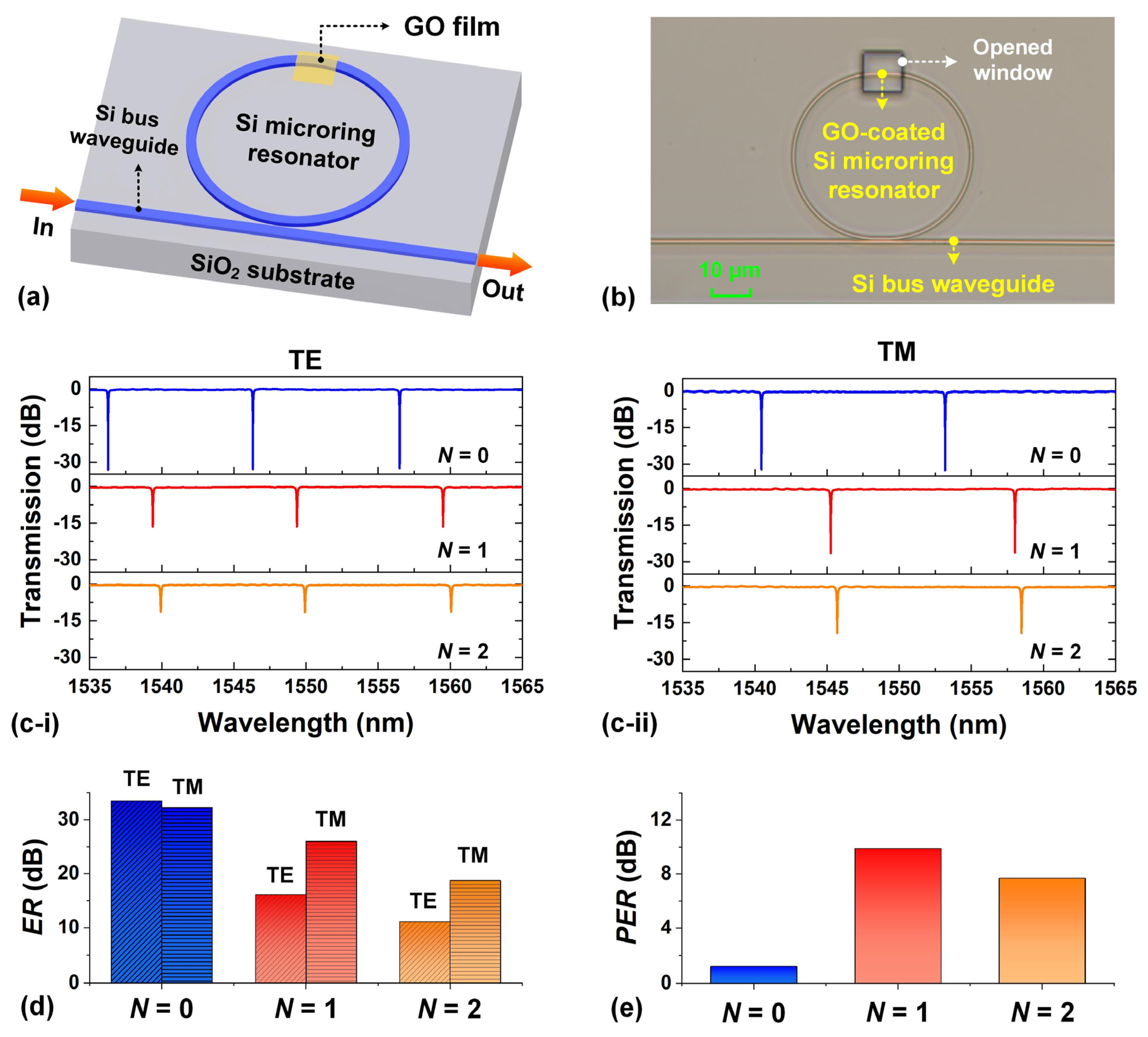
By scanning the wavelength of a CW light coupled into the bus waveguides, we measured the TE- and TM-polarized transmission spectra of the MRRs. Figure 5c shows the measured spectra for the hybrid MRRs with 1 and 2 layers of GO, together with those for the uncoated MRR for comparison. For all the measured spectra, the input CW power remained constant at Pin = ~-10 dBm. Figure 5d shows the extinction ratios (ER’s) of these MRRs extracted from Figure 5c. For the uncoated MRR, the ERs for TE and TM polarizations were ~33 dB and ~32 dB, respectively. In contrast, the ERs decreased to ~16 dB and ~26 dB for the 1-layer device, and ~11 dB and ~19 dB for the 2-layer device. Figure 5e shows the polarization extinction ratio (PER) calculated from Figure 5d, which is defined as the absolute difference between the ER’s of the TE- and TM-polarized resonances. As can be seen, the uncoated MRR exhibited negligible polarization selectivity, with its PER being less than ~1 dB. In contrast, the hybrid devices with 1 and 2 layers of GO exhibited PER values of ~10 dB and ~8 dB, respectively, highlighting their high polarization selectivity. Compared to the device with 2 layers of GO, the device with 1 layer of GO exhibited a higher PER. This is mainly induced by a more significant decrease in the TM-polarized ER for the device with a thicker GO film.
In Figure 6, we characterize the power-dependent response for the polarization-selective MRR. We employed two CW inputs in our measurements. On CW beam provided a pump into one of the MRR’s tuned to a resonance. Its wavelength was adjusted near the resonance until a thermal equilibrium state was reached. Next, a second lower CW power beam at -10 dBm was used to probe the MRR’s transmission spectra. In contrast to directly using a high-power CW pump to scan the spectra, the probe minimized any resonance lineshape asymmetry due to optical bistability,[41,42] thus enabling more precise characterization of the ERs.
Figure 6.
(a) TE- and TM-polarized ER versus input power (Pin) for the hybrid MRR with 1 layer of GO (N = 1). (b) PER extracted from (a). (c) Fit k’s obtained from the MRR experiment and the waveguide (WG) experiment. (d) Ratios of k values for TE and TM polarizations (kTE / kTM) extracted from (c).
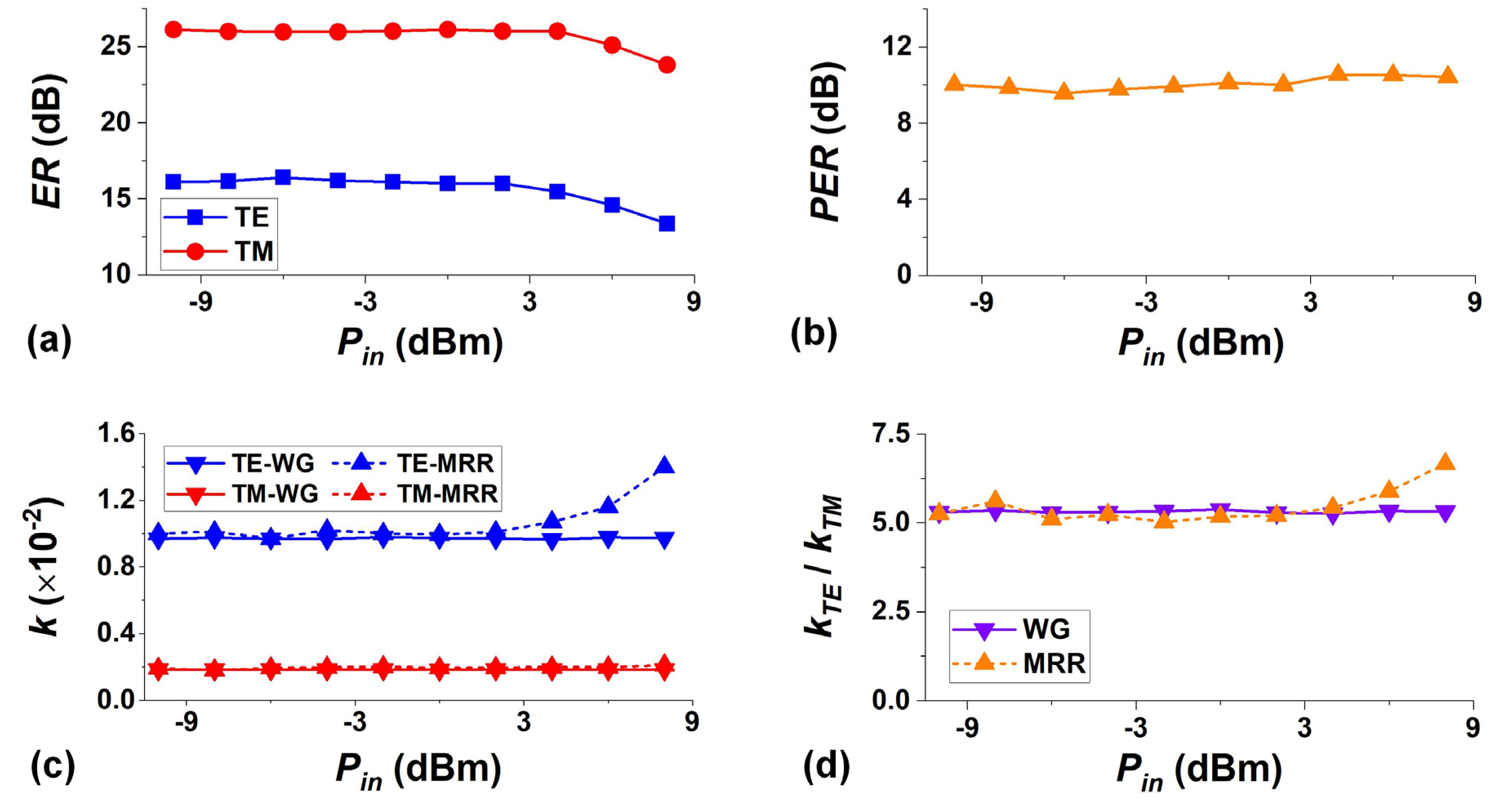
In Figure 6a, we plot TE- and TM-polarized ER’s versus input pump power Pin for the hybrid MRR with 1 layer of GO. Figure 6b shows the PER calculated from Figure 6a. For TE polarization in Figure 6a, the ER remains constant at ~17 dB when Pin ≤ ~0 dBm. When Pin > ~0 dBm, there is an obvious decrease in the ER resulting from an increased loss induced by photo-thermal reduction of GO. For TM polarization, the ER remains constant at ~26 dB when Pin ≤ 4 dBm, followed by a decrease when Pin > 4 dBm. Compared to TE polarization, TM polarization exhibits a higher power threshold at which the ER starts to decrease. This further confirms the relatively weak photo-thermal effects for TM polarization. In Figure 6b, the higher power threshold for TM polarization also leads to a slight increase in the PER when ~0 dBm < Pin < ~4 dBm. We also note that the PER slightly decreases when Pin > ~4 dBm. This is mainly induced by a more dramatic decrease in the ER for TM polarization, which has a higher value (in dB) compared to TE polarization. It is also worth mentioning that the results in Figure 6 were measured at one of the MRRs’ resonance wavelengths near 1550 nm. Similar phenomena were also observed at other resonance wavelengths within the maximum tuning range of our CW laser (i.e., 1500 ‒ 1600 nm).
By using the scattering matrix method[43,44,45,46,47,48,49,50,51] to fit the measured transmission spectra, we obtained the PL’s of the GO-coated segment in the hybrid MRR. The k’s of 2D GO films were further extracted from the obtained PL’s using the same method as in Figure 4a. Figure 6c shows the k’s of 2D GO films versus Pin, and Figure 6b shows the ratios of the TE- to TM-polarized k values calculated from Figure 6c. For comparison, we also show the corresponding results obtained from the waveguide experiment in Figure 4d. In Figure 6c, the k values obtained from the MRR experiment match closely with those obtained from the waveguide experiment, reflecting the consistency of our GO film fabrication process. As the input power increases, the k obtained from the MRR experiment exhibits a more significant increase, indicating that there was more significant photo-thermal reduction of GO in the hybrid MRR due to the resonant enhancement effect. When Pin ≤ 0 dBm, the ratio in Figure 6d remains nearly constant at ~5.3, which is consistent with that in Figure 4(a-iii). For Pin > 0 dBm, the ratio increases with Pin, achieving a maximum value of ~6.9 at Pin = ~8 dBm. In contrast, the ratio obtained from the hybrid waveguide was still ~5.3 at the same input power.
In summary, waveguide and MRR polarizers are demonstrated by integrating 2D GO films onto Si photonic devices. We fabricate hybrid devices with precise control over the thicknesses and lengths of GO films and perform detailed measurements with them. By optimizing the GO film thicknesses, lengths, and Si waveguide widths, up to ~17-dB PDL and ~10-dB PER are achieved for the waveguide and MRR polarizers, respectively. The dependence of the polarizers’ response on the wavelength and power of input light is also characterized, showing a broad operation bandwidth over ~100 nm as well as polarization selectivity improvement enabled by photo-thermal changes in GO. Finally, we find that the anisotropy in the loss of GO films dominates the polarization selectivity of these polarizers by fitting the experimental results with theoretical simulations. Our study provides an attractive approach for implementing high-performance optical polarizers by integrating 2D GO films onto Si photonic devices and complements the recent advances made in GO coated nanophotonic devices for linear and nonlinear optics. [52,53,54,55,56,57,58,59,60,61,62,63,64,65,66,67,68,69,70,71,72,73,7]
Conflict of Interest
The authors have no conflicts to disclose.
References
- Yan, Y.; Xie, G.; Lavery, M.P.J.; Huang, H.; Ahmed, N.; Bao, C.; Ren, Y.; Cao, Y.; Li, L.; Zhao, Z.; Molisch, A.F.; Tur, M.; Padgett, M.J.; Willner, A.E. High-capacity millimetre-wave communications with orbital angular momentum multiplexing. Nature Communications, 2014, 5, 4876. [Google Scholar] [CrossRef]
- Dai, D.; Liu, L.; Gao, S.; Xu, D.-X.; He, S. Polarization management for silicon photonic integrated circuits. Laser & Photonics Reviews, 2013, 7, 303–328. [Google Scholar]
- Chu, J.; Zhao, K.; Zhang, Q.; Wang, T. Construction and performance test of a novel polarization sensor for navigation. Sensors and Actuators A: Physical, 2008, 148, 75–82. [Google Scholar] [CrossRef]
- Thilak, V.; Voelz, D.G.; Creusere, C.D. Polarization-based index of refraction and reflection angle estimation for remote sensing applications. Applied Optics, 2007, 46, 7527–7536. [Google Scholar] [CrossRef]
- Lee, C.-T.; Lin, H.-Y.; Tsai, C.-H. Designs of broadband and wide-view patterned polarizers for stereoscopic 3D displays. Optics Express, 2010, 18, 27079–27094. [Google Scholar] [CrossRef]
- Kim, S.H.; Park, J.-D.; Lee, K.-D. Fabrication of a nano-wire grid polarizer for brightness enhancement in liquid crystal display. Nanotechnology, 2006, 17, 4436. [Google Scholar] [CrossRef]
- Cho, Y.T. Fabrication of wire grid polarizer for spectroscopy application: From ultraviolet to terahertz. Applied Spectroscopy Reviews, 2018, 53, 224–245. [Google Scholar] [CrossRef]
- He, C.; He, H.; Chang, J.; Chen, B.; Ma, H.; Booth, M.J. Polarisation optics for biomedical and clinical applications: a review. Light: Science & Applications, 2021, 10, 194. [Google Scholar]
- Han, Y.; Li, G. Coherent optical communication using polarization multiple-input-multiple-output. Optics Express, 2005, 13, 7527–7534. [Google Scholar] [CrossRef]
- Zhang, Z.; Gan, J.; Yang, T.; Wu, Y.; Li, Q.; Xu, S.; Yang, Z. All-fiber mode-locked laser based on microfiber polarizer. Optics Letters, 2015, 40, 784–787. [Google Scholar] [CrossRef]
- Serkowski, K.; Mathewson, D.; Ford, V. Wavelength dependence of interstellar polarization and ratio of total to selective extinction. Astrophysical Journal, 1975, 196, 261–290. [Google Scholar] [CrossRef]
- Wang, T.J.; He, Q.Y.; Gao, J.Y.; Jiang, Y.; Kang, Z.H.; Sun, H.; Yu, L.S.; Yuan, X.F.; Wu, J. Efficient electrooptically Q-switched Er:Cr:YSGG laser oscillator-amplifier system with a Glan-Taylor prism polarizer. Laser Physics, 2006, 16, 1605–1609. [Google Scholar] [CrossRef]
- Saitoh, E.; Kawaguchi, Y.; Saitoh, K.; Koshiba, M. TE/TM-Pass Polarizer Based on Lithium Niobate on Insulator Ridge Waveguide. IEEE Photonics Journal, 2013, 5, 6600610–6600610. [Google Scholar] [CrossRef]
- Rahnama, A.; Dadalyan, T.; Aghdami, K.M.; Galstian, T.; Herman, P.R. In-Fiber Switchable Polarization Filter Based on Liquid Crystal Filled Hollow-Filament Bragg Gratings. Advanced Optical Materials, 2021, 9, 2100054. [Google Scholar] [CrossRef]
- Wang, J.; Yang, J.-Y.; Fazal, I.M.; Ahmed, N.; Yan, Y.; Huang, H.; Ren, Y.; Yue, Y.; Dolinar, S.; Tur, M. Terabit free-space data transmission employing orbital angular momentum multiplexing. Nature photonics, 2012, 6, 488–496. [Google Scholar] [CrossRef]
- Bozinovic, N.; Yue, Y.; Ren, Y.; Tur, M.; Kristensen, P.; Huang, H.; Willner, A.E.; Ramachandran, S. Terabit-scale orbital angular momentum mode division multiplexing in fibers. science, 2013, 340, 1545–1548. [Google Scholar] [CrossRef]
- Dai, D.; Wang, Z.; Julian, N.; Bowers, J.E. Compact broadband polarizer based on shallowly-etched silicon-on-insulator ridge optical waveguides. Optics Express, 2010, 18, 27404–27415. [Google Scholar] [CrossRef]
- Huang, Y.; Zhu, S.; Zhang, H.; Liow, T.-Y.; Lo, G.-Q. CMOS compatible horizontal nanoplasmonic slot waveguides TE-pass polarizer on silicon-on-insulator platform. Optics Express, 2013, 21, 12790–12796. [Google Scholar] [CrossRef]
- Li, Z.; Xu, B.; Liang, D.; Pan, A. Polarization-Dependent Optical Properties and Optoelectronic Devices of 2D Materials. Research, 2020; 2020. [Google Scholar]
- Bao, Q.; Zhang, H.; Wang, B.; Ni, Z.; Lim, C.H.Y.X.; Wang, Y.; Tang, D.Y.; Loh, K.P. Broadband graphene polarizer. Nature Photonics, 2011, 5, 411–415. [Google Scholar] [CrossRef]
- Lin, H.; Song, Y.; Huang, Y.; Kita, D.; Deckoff-Jones, S.; Wang, K.; Li, L.; Li, J.; Zheng, H.; Luo, Z.; Wang, H.; Novak, S.; Yadav, A.; Huang, C.-C.; Shiue, R.-J.; Englund, D.; Gu, T.; Hewak, D.; Richardson, K.; Kong, J.; Hu, J. Chalcogenide glass-on-graphene photonics. Nature Photonics, 2017, 11, 798–805. [Google Scholar] [CrossRef]
- Kim, J.T.; Choi, C.-G. Graphene-based polymer waveguide polarizer. Optics Express, 2012, 20, 3556–3562. [Google Scholar] [CrossRef]
- Pei, C.; Yang, L.; Wang, G.; Wang, Y.; Jiang, X.; Hao, Y.; Li, Y.; Yang, J. Broadband Graphene/Glass Hybrid Waveguide Polarizer. IEEE Photonics Technology Letters, 2015, 27, 927–930. [Google Scholar] [CrossRef]
- Lim, W.H.; Yap, Y.K.; Chong, W.Y.; Pua, C.H.; Huang, N.M.; De La Rue, R.M.; Ahmad, H. Graphene oxide-based waveguide polariser: From thin film to quasi-bulk. Optics Express, 2014, 22, 11090–11098. [Google Scholar] [CrossRef]
- Wu, J.; Yang, Y.; Qu, Y.; Xu, X.; Liang, Y.; Chu, S.T.; Little, B.E.; Morandotti, R.; Jia, B.; Moss, D.J. Graphene Oxide Waveguide and Micro-Ring Resonator Polarizers. Laser & Photonics Reviews, 2019, 13, 1900056. [Google Scholar]
- Tan, Y.; He, R.; Cheng, C.; Wang, D.; Chen, Y.; Chen, F. Polarization-dependent optical absorption of MoS2 for refractive index sensing. Scientific Reports, 2014, 4, 7523. [Google Scholar] [CrossRef]
- Sathiyan, S.; Ahmad, H.; Chong, W.Y.; Lee, S.H.; Sivabalan, S. Evolution of the Polarizing Effect of $\text{MoS}_{2}$. IEEE Photonics Journal, 2015, 7, 1–10. [Google Scholar] [CrossRef]
- Zhou, F.; Zhang, J. Polarization-Independent Black-Phosphorus Polarizer in Visible Regime. IEEE Photonics Technology Letters, 2017, 29, 1923–1926. [Google Scholar] [CrossRef]
- Wu, J.; Lin, H.; Moss, D.J.; Loh, K.P.; Jia, B. Graphene oxide for photonics, electronics and optoelectronics. Nature Reviews Chemistry, 2023, 7, 162–183. [Google Scholar] [CrossRef]
- Wu, J.; Jia, L.; Zhang, Y.; Qu, Y.; Jia, B.; Moss, D.J. Graphene Oxide for Integrated Photonics and Flat Optics. Advanced Materials, 2021, 33, 2006415. [Google Scholar] [CrossRef]
- Yang, Y.; Zhang, Y.; Zhang, J.; Zheng, X.; Gan, Z.; Lin, H.; Hong, M.; Jia, B. Graphene Metamaterial 3D Conformal Coating for Enhanced Light Harvesting. ACS Nano, 2023, 17, 2611–2619. [Google Scholar] [CrossRef]
- Loh, K.P.; Bao, Q.; Eda, G.; Chhowalla, M. Graphene oxide as a chemically tunable platform for optical applications. Nature Chemistry, 2010, 2, 1015–1024. [Google Scholar] [CrossRef]
- El-Kady, M.F.; Strong, V.; Dubin, S.; Kaner, R.B. Laser Scribing of High-Performance and Flexible Graphene-Based Electrochemical Capacitors. Science, 2012, 335, 1326–1330. [Google Scholar] [CrossRef]
- Bonaccorso, F.; Sun, Z.; Hasan, T.; Ferrari, A.C. Graphene photonics and optoelectronics. Nature Photonics, 2010, 4, 611–622. [Google Scholar] [CrossRef]
- Phare, C.T.; Lee, Y.-H.D.; Cardenas, J.; Lipson, M. Graphene electro-optic modulator with 30 GHz bandwidth. Nature photonics, 2015, 9, 511–514. [Google Scholar] [CrossRef]
- Calafell, I.A.; Rozema, L.A.; Iranzo, D.A.; Trenti, A.; Jenke, P.K.; Cox, J.D.; Kumar, A.; Bieliaiev, H.; Nanot, S.; Peng, C.; Efetov, D.K.; Hong, J.-Y.; Kong, J.; Englund, D.R.; de Abajo, F.J.G.; Koppens, F.H.L.; Walther, P. Giant enhancement of third-harmonic generation in graphene–metal heterostructures. Nature Nanotechnology, 2021, 16, 318–324. [Google Scholar] [CrossRef]
- Lin, H.; Sturmberg, B.C.P.; Lin, K.-T.; Yang, Y.; Zheng, X.; Chong, T.K.; de Sterke, C.M.; Jia, B. A 90-nm-thick graphene metamaterial for strong and extremely broadband absorption of unpolarized light. Nature Photonics, 2019, 13, 270–276. [Google Scholar] [CrossRef]
- Dai, D.; Bauters, J.; Bowers, J.E. Passive technologies for future large-scale photonic integrated circuits on silicon: polarization handling, light non-reciprocity and loss reduction. Light: Science & Applications 2020, 1, 1906563. [Google Scholar]
- Zhang, Y.; Wu, J.; Jia, L.; Qu, Y.; Yang, Y.; Jia, B.; Moss, D.J. Graphene Oxide for Nonlinear Integrated Photonics. Laser & Photonics Reviews, 2023, 17, 2200512. [Google Scholar]
- Smith, P.W.; Tomlinson, W.J. Bistable optical devices promise subpicosecond switching. IEEE Spectrum, 1981, 18, 26–33. [Google Scholar] [CrossRef]
- Gibbs, H. , Optical bistability: controlling light with light: Elsevier, 2012.
- Arianfard, H.; Juodkazis, S.; Moss, D.J.; Wu, J. Sagnac interference in integrated photonics. Applied Physics Reviews, 2023, 10, 011309. [Google Scholar] [CrossRef]
- Arianfard, H.; Wu, J.; Juodkazis, S.; Moss, D.J. Optical analogs of Rabi splitting in integrated waveguide-coupled resonators”, Advanced Physics Research 2023, 2, 2200123. 2. [CrossRef]
- Arianfard, H.; Wu, J.; Juodkazis, S.; Moss, D.J. Spectral shaping based on optical waveguides with advanced Sagnac loop reflectors”, Paper No. PW22O-OE201-20, SPIE-Opto, Integrated Optics: Devices, Materials, and Technologies XXVI, SPIE Photonics West, San Francisco CA January 22- 27 (2022). [CrossRef]
- Arianfard, H.; Wu, J.; Juodkazis, S.; Moss, D.J. Spectral Shaping Based on Integrated Coupled Sagnac Loop Reflectors Formed by a Self-Coupled Wire Waveguide”, IEEE Photonics Technology Letters 2021, 33, 680–683. [CrossRef]
- Arianfard, H.; Wu, J.; Juodkazis, S.; Moss, D.J. Three Waveguide Coupled Sagnac Loop Reflectors for Advanced Spectral Engineering”, Journal of Lightwave Technology 2021, 39, 3478–3487. [CrossRef]
- Arianfard, H.; Wu, J.; Juodkazis, S.; Moss, D.J. Advanced Multi-Functional Integrated Photonic Filters based on Coupled Sagnac Loop Reflectors”, Journal of Lightwave Technology 2021, 39, 1400–1408. [CrossRef]
- Arianfard, H.; Wu, J.; Juodkazis, S.; Moss, D.J. Advanced multi-functional integrated photonic filters based on coupled Sagnac loop reflectors”, Paper 11691-4, PW21O-OE203-44, Silicon Photonics XVI, SPIE Photonics West, San Francisco CA March 6-11 (2021). doi.org/10.1117/12. 6 March 2584. [Google Scholar]
- Wu, J.; Moein, T.; Xu, X.; Moss, D.J. Advanced photonic filters via cascaded Sagnac loop reflector resonators in silicon-on-insulator integrated nanowires”, Applied Physics Letters Photonics 2018, 3, 046102. [CrossRef]
- Wu, J.; Moein, T.; Xu, X.; Ren, G.; Mitchell, A.; Moss, D.J. Micro-ring resonator quality factor enhancement via an integrated Fabry-Perot cavity”, Applied Physics Letters Photonics 2017, 2, 056103. [CrossRef]
- et al. Enhanced Kerr nonlinearity and nonlinear figure of merit in silicon nanowires integrated with 2d graphene oxide films. ACS Appl. Mater. Interfaces 2020, 12, 33094–33103. [Google Scholar] [CrossRef]
- et al. Enhanced four-wave mixing in silicon nitride waveguides integrated with 2d layered graphene oxide films. Advanced Optical Materials 2020, 8, 2001048. [Google Scholar] [CrossRef]
- et al. Highly nonlinear BiOBr nanoflakes for hybrid integrated photonics. APL Photonics 2019, 4, 090802. [Google Scholar] [CrossRef]
- Zhang, Y.; Wu, J.; Yang, Y.; Qu, Y.; Jia, L.; El Dirani, H.; Kerdiles, S.; Sciancalepore, C.; Demongodin, P.; Grillet, C.; Monat, C.; Jia, B.; Moss, D.J. Enhanced supercontinuum generated in SiN waveguides coated with GO films”, Advanced Materials Technologies 2023, 8, 2201796. [CrossRef]
- Zhang, Y.; Wu, J.; Jia, L.; Qu, Y.; Jia, B.; Moss, D.J. Graphene oxide for nonlinear integrated photonics”, Laser and Photonics Reviews 2023, 17, 2200512. [CrossRef]
- Qu, Y.; Wu, J.; Zhang, Y.; Yang, Y.; Jia, L.; Jia, B.; Moss, D.J. Photo thermal tuning in GO-coated integrated waveguides”, Micromachines 2022, 13, 1194.
- Zhang, Y.; Wu, J.; Yang, Y.; Qu, Y.; El Dirani, H.; Crochemore, R.; Sciancalepore, C.; Demongodin, P.; Grillet, C.; Monat, C.; Jia, B.; Moss, D.J. Enhanced self-phase modulation in silicon nitride waveguides integrated with 2D graphene oxide films”, IEEE Journal of Selected Topics in Quantum Electronics 2023, 29, 5100413. [CrossRef]
- Zhang, Y.; Wu, J.; Yang, Y.; Qu, Y.; Jia, L.; Jia, B.; Moss, D.J. Enhanced spectral broadening of femtosecond optical pulses in silicon nanowires integrated with 2D graphene oxide films”, Micromachines 2022, 13, 756. [CrossRef]
- Hu, J.; Wu, J.; Liu, W.; Jin, D.; El Dirani, H.; Kerdiles, S.; Sciancalepore, C.; Demongodin, P.; Grillet, C.; Monat, C.; Huang, D.; Jia, B.; Moss, D.J. 2D graphene oxide: a versatile thermo-optic material”, Advanced Functional Materials 2024.
- Qu, Y.; Wu, J.; Zhang, Y.; Yang, Y.; Jia, L.; El Dirani, H.; Kerdiles, S.; Sciancalepore, C.; Demongodin, P.; Grillet, C.; Monat, C.; Jia, B.; Moss, D.J. Optical parametric amplifiers based on silicon nitride waveguides integrated with 2D graphene oxide films”, Light: Advanced Manufacturing 2023, 4, 39. 4. [CrossRef]
- Jin, D.; Liu, W.; Jia, L.; Hu, J.; Huang, D.; Wu, J.; Jia, B.; Moss, D.J. Strong and layer-dependent nonlinear optical absorption in 2D layered MXene films”, Small Science (2024).
- Jia, L.; Wu, J.; Zhang, Y.; Qu, Y.; Jia, B.; Chen, Z.; Moss, D.J. Fabrication Technologies for the On-Chip Integration of 2D Materials”, Small: Methods 2022, 6, 2101435. [CrossRef]
- Zhang, Y.; Wu, J.; Qu, Y.; Jia, L.; Jia, B.; Moss, D.J. Design and optimization of four-wave mixing in microring resonators integrated with 2D graphene oxide films”, Journal of Lightwave Technology 2021, 39, 6553–6562. [CrossRef]
- Zhang, Y.; Wu, J.; Qu, Y.; Jia, L.; Jia, B.; Moss, D.J. Optimizing the Kerr nonlinear optical performance of silicon waveguides integrated with 2D graphene oxide films”, Journal of Lightwave Technology 2021, 39, 4671–4683. [CrossRef]
- Qu, Y.; Wu, J.; Zhang, Y.; Liang, Y.; Jia, B.; Moss, D.J. Analysis of four-wave mixing in silicon nitride waveguides integrated with 2D layered graphene oxide films”, Journal of Lightwave Technology 2021, 39, 2902–2910. [CrossRef]
- Qu, Y.; Wu, J.; Zhang, Y.; Jia, L.; Yang, Y.; Xu, X.; Chu, S.T.; Little, B.E.; Morandotti, R.; Jia, B.; Moss, D.J. Graphene oxide for enhanced optical nonlinear performance in CMOS compatible integrated devices”, Paper No. 11688-30, PW21O-OE109-36, 2D Photonic Materials and Devices IV, SPIE Photonics West, San Francisco CA -11 (2021). doi.org/10.1117/12. 6 March 2583. [Google Scholar]
- Qu, Y.; Wu, J.; Yang, Y.; Zhang, Y.; Liang, Y.; El Dirani, H.; Crochemore, R.; Demongodin, P.; Sciancalepore, C.; Grillet, C.; Monat, C.; Jia, B.; Moss, D.J. Enhanced nonlinear four-wave mixing in silicon nitride waveguides integrated with 2D layered graphene oxide films”, Advanced Optical Materials 2020, 8, 2001048. [CrossRef]
- Zhang, Y.; Qu, Y.; Wu, J.; Jia, L.; Yang, Y.; Xu, X.; Jia, B.; Moss, D.J. Enhanced Kerr nonlinearity and nonlinear figure of merit in silicon nanowires integrated with 2D graphene oxide films”, ACS Applied Materials and Interfaces 2020, 12, 33094−33103. [CrossRef]
- Wu, J.; Yang, Y.; Qu, Y.; Xu, X.; Liang, Y.; Chu, S.T.; Little, B.E.; Morandotti, R.; Jia, B.; Moss, D.J. Graphene oxide waveguide polarizers and polarization selective micro-ring resonators”, Paper 11282-29, SPIE Photonics West, San Francisco, CA, 4 - 7 February (2020). [CrossRef]
- Yang, Y.; Wu, J.; Xu, X.; Chu, S.T.; Little, B.E.; Morandotti, R.; Jia, B.; Moss, D.J. Enhanced four-wave mixing in graphene oxide coated waveguides”, Applied Physics Letters Photonics 2018, 3, 120803. [CrossRef]
- Jia, L.; Qu, Y.; Wu, J.; Zhang, Y.; Yang, Y.; Jia, B.; Moss, D.J. Third-order optical nonlinearities of 2D materials at telecommunications wavelengths”, Micromachines 2023, 14, 307. [CrossRef]
- Jia, L.; Cui, D.; Wu, J.; Feng, H.; Yang, T.; Yang, Y.; Du, Y.; Hao, W.; Jia, B.; Moss, D.J. BiOBr nanoflakes with strong nonlinear optical properties towards hybrid integrated photonic devices”, Applied Physics Letters Photonics 2019, 4, 090802. [CrossRef]
- Jia, L.; Wu, J.; Yang, Y.; Du, Y.; Jia, B.; Moss, D.J. Large Third-Order Optical Kerr Nonlinearity in Nanometer-Thick PdSe2 2D Dichalcogenide Films: Implications for Nonlinear Photonic Devices”, ACS Applied Nano Materials 2020, 3, 6876–6883. [CrossRef]
Disclaimer/Publisher’s Note: The statements, opinions and data contained in all publications are solely those of the individual author(s) and contributor(s) and not of MDPI and/or the editor(s). MDPI and/or the editor(s) disclaim responsibility for any injury to people or property resulting from any ideas, methods, instructions or products referred to in the content. |
© 2024 by the author. Licensee MDPI, Basel, Switzerland. This article is an open access article distributed under the terms and conditions of the Creative Commons Attribution (CC BY) license (https://creativecommons.org/licenses/by/4.0/).
Copyright: This open access article is published under a Creative Commons CC BY 4.0 license, which permit the free download, distribution, and reuse, provided that the author and preprint are cited in any reuse.


