Preprint
Article

Analog Implementation of a Spiking Neuron with Memristive Synapses for Deep Learning Processing

Altmetrics

Downloads

138

Views

72

Comments

0

A peer-reviewed article of this preprint also exists.

Submitted:

30 May 2024

Posted:

31 May 2024

You are already at the latest version

Alerts
Abstract
Analog neuromorphic prototyping is crucial for creating spiking neuron models that use memristive devices as synapses to design integrated circuits that leverage on-chip parallel deep neural networks. These models mimic how biological neurons in the brain communicate through electrical potentials. Doing so enables more powerful and efficient functionality than traditional artificial neural networks that run on von Neumann computers or graphic processing unit-based platforms. This technology can accelerate deep learning processing, aiming to exploit the brain’s unique features of asynchronous and event-driven processing by leveraging neuromorphic hardware’s inherent parallelism and analog computation capabilities. Therefore, this paper presents the design and implementation of a leaky integrate and fire neuron prototype implemented with commercially available components on a PCB board. Simulations conducted in LTSpice agree well with the electrical test measurements. The results demonstrate that this design can be employed to interconnect many boards to build layers of physical spiking neurons, interconnected with spike-timing-dependent plasticity as the primary learning algorithm, contributing to the realization of experiments in the early stage of adopting neuromorphic computing.
Keywords: 
Subject: Computer Science and Mathematics  -   Artificial Intelligence and Machine Learning

1. Introduction

In recent years, generative AI has become the most popular application of artificial intelligence (AI) for the general public. This technology has showcased unprecedented capabilities in text [1], video, and image generation [2]; however, these advancements come with a significant caveat: the power consumption required to operate. The power consumption expended during GPT-3 training is estimated at around 1287 MWh [3]. This energy consumption is deemed unsustainable and will only increase as AI-enabled devices and services increase, consequently scaling to more complex generative models. To address the problem, novel computing architectures for AI are being developed, showing a dramatic increase in power efficiency. The area of computing that deals with novel computing architectures is referred to as neuromorphic computing [4]. Neuromorphic computing draws inspiration from the human brain to replicate its functions and structures on complementary metal-oxide semiconductor (CMOS) technology devices, using high neuron connectivity, sparse processing, and distributed computing.
This hardware approach utilizes the analog domain to handle multiple inputs and react asynchronously, achieving this by employing a bioplausible realization of neuron cells at the silicon level, called spiking neurons [5]. These neurons can process information sparsely with minimal power consumption, resist noise, and combine memory and processing on a single silicon die (edge computing). They use only a few milliwatts of power while providing parallel processing capabilities and integrating thousands of neurons. Another missing link in the search for efficient computing for AI is the implementation of artificial synapses. Synapses are the space between neurons that allow the transmission of information between neurons and reinforce the activity between them [6]. Nowadays, many device alternatives with different materials have been proposed to achieve this end goal, such as phase change memories (PCM) [7], floating gate transistors [8], and memristors [9].
Memristors are two-terminal electrical devices that exhibit a functional relationship between charge and flux. When a voltage difference, V ( t ) , is applied across their terminals, it results in the movement of charged dopants between doped and undoped regions, causing a change in the device’s resistance value [10]. These devices can process and store information simultaneously while utilizing nano-amperes of current; this is useful in computing systems where this process is called multiply-accumulate (MAC) operation and is related to matrix multiplication and storage; these devices can reduce the energy consumption of computing systems while improving the reliability [11].
This paper presents an analog hardware implementation of a spiking neuron architecture, employing commercial components and memristive devices acting as artificial synapses. Section 1 provides a brief introduction. Section 2 presents the neuron and synaptic modeling, as well as some concepts regarding the synaptic weight adjustment in neurons and the electrical characteristics of the proposed neuron. Section 3 presents the simulation results, the methodology utilized to characterize the neuron, the results obtained with the physical implementation, and the synaptic weight adjustment. Lastly, section 4 discusses results and future work.

2. Materials and Methods

In this section, we will review the modeling of neurons and memristive synapses, the concept of weight adjustment in neurons, and the learning mechanisms. Lastly, we will cover the implementation of spiking neurons and the selection of components.

2.1. Neuron Modeling

Spiking neurons are relevant in computational neuroscience and artificial neural networks. They aim to replicate the behavior of neurons in the brain, where information is transmitted through brief electrical pulses, known as spikes or action potentials. These spikes act as the fundamental units of communication between neurons. In a spiking neuron model, the neuron’s membrane potential changes in response to inputs from other neurons or outside stimuli. Once the membrane potential reaches a specific threshold, the neuron generates an output spike, which is transmitted to other connected neurons. After spiking, the membrane potential resets to a resting state, and the process starts anew.
The Hodgkin & Huxley model [12] accurately describes the behavior of neurons through four differential equations. This has high fidelity with respect to biological neurons’ behavior, but it comes at a high computational cost. The Leak-Integrate-and-Fire [13] is a simpler model compared with the Hodgkin & Huxley, but it maintains the overall behavior of the neurons. This behavior is modeled by equation 1, where v m ( t ) is the membrane’s potential, E L is the membrane’s potential at rest, τ m is the time constant of charging of the neuron which is represented by R m C m ; where R m is the membrane’s resistance and C m is the membrane’s capacitance. I s y n ( t ) is the excitatory input current of the neuron. This current charges the neuron’s capacitance, modifying the neuron’s voltage, v m ( t ) . Once this voltage surpasses a threshold v t h , an output spike is generated, and v m ( t ) takes the value of E L .
τ m d v m ( t ) d t = E L v m ( t ) + R m I s y n ( t )

2.2. Memristor modeling

Memristors are two-terminal electronic components that exhibit a relationship between the time integrals of current and voltage across them. They were theorized by Leon Chua in 1971 [10] and are considered the fourth fundamental passive circuit element alongside resistors, capacitors, and inductors. Electrical modeling of memristors involves mathematically representing their behavior to understand and predict their performance in circuits. The first mathematical models for memristors were developed from a memristor’s equivalent electrical circuit consisting of two resistors connected in series [14]; improvements were proposed with the use of window functions with adjustable parameters [15]; this improved the convergence of the model in corner cases where the regions between the doped and undoped semiconductors reach the limit of the thin dielectric layer.

2.2.1. Vourkas Memristor Model

In this Subsection, the macro model for a memristor proposed by [16] will be explained. The schematic diagram of a memristor macromodel is depicted in Figure 1(a). Figure 1(b) represents the typical electrical symbol of a memristor. The cross-section of a memristor is shown in Figure 1(c), in which a region of insulating material of TiO2 separates two metal plates that form the terminals of the device.
Two regions of material with different conductivity are distinguished inside the thin insulating material. The region denoted by L o represents the total thickness of the insulating material. On the other hand, L is the distance between the border of the two regions of the TiO2 composite material, with respect to the border with the lower terminal (metallic contact). The upper region of the TiO2 material develops a low resistance of R value due to the vacancies of oxygen atoms that occur due to the migration of atoms in response to the effect of the intense electric field present in the structure. The upper region is, therefore, considered a doped region extending a distance with a value of L 0 L . On the other hand, the lower region that receives the oxygen atoms behaves as an insulator and develops a very high resistance, with a value denoted by R t . In the region with thickness L, a charge transport process develops through the tunneling mechanism, coupled in series with the upper region ( L 0 L ), with a lower resistive value. The resistance values in both regions are very different, with a notable difference of R t R , so the Vourkas model focuses on determining only the value of R t and is considered to develop a proportional resistive value to the width of the tunnel barrier L and that the electron conduction would be dominated by the effective width of the tunnel barrier, which varies as a function of time and the magnitude of voltage applied between the terminals of the device. Also, it is considered that the border between the two regions and, therefore, the value of L changes depending on the migration of oxygen deficiencies due to the effect of an electrical potential applied between the terminals.
The macromodel behavior proposed by [16] is defined by the Equation 2:
I ( t ) = G ( L , t ) V M ( t )
where I is the current that flows in the memristor, G is the conductance, and V M is the voltage applied between the top and the bottom terminals. Next, the rate of change of L is defined by:
L ˙ = f ( V M , t )
From quantum mechanics, an expression can be determined for the tunnel resistance, R t , whose value is inversely proportional to the product of the transmission coefficient, T 0 , and the effective density of states, N e f f , from the material TiO2. T 0 is simultaneously a function of the voltage applied between the terminals of the memristor ( V M ), which provides sufficient energy for the electrons to pass through the thin film of the undoped material L. On the other hand, the resistance R t is exponentially proportional to the width of the tunneling barrier (L). Therefore, the tunnel resistance R t is defined by the equation 4:
R t ( V M ) = e x p 2 k V M · L N e f f · T 0 , V M
By making a change of variable, we can rewrite the equation 4, as follows:
R t ( V M ) = f 0 · e x p 2 L V M , t L V M , t
In equation 5, a new voltage-dependent parameter, L V M , is defined, which replaces the voltage-dependent parameters: T 0 , and k V M . Equation 5, calculates the value of the resistance of a memristor, subject to the state variable L. The adjustment variable f 0 functions to represent the specific parameters of the material and aspects related to the geometry. The heuristic equation 6 defines the new variable L ( V M , t ) , as well as its minimum and maximum intervals.
L ( V M , t ) = L 0 · ( 1 m r ( V M , t ) )
Equation 6, delivers the expected response of L, as a function of time, t, and V M . Therefore, L 0 represents the largest dimension that L can reach. On the other hand, the voltage-dependent parameter, denoted as r ( V M , t ) , and the term m (adjustment parameter) are used to determine the boundary of the tunnel barrier width. Equation (6), determines the initial and current position of L, being defined between the limits of the two boundary values. The parameter r ( V M , t ) defines both the dynamics of the device and its current state. Its value must be maintained between a valid interval. The on-and-off dynamics of the memristor depend on the structure of the device, mainly on the type of oxide used, which determines the drift speed of the ions that move along L 0 , due to the effect of the electric field. These dynamics are incorporated into the macromodel assuming that the change of L is fast if V M exceeds a certain positive threshold voltage, denoted as V S E T ( V S E T < V M ), or a negative threshold voltage V R E S E T ( V M < V R E S E T ). Otherwise, if V M is below both thresholds, e.g. V R E S E T V M V S E T , the change in L, and therefore, in the memristance is practically zero. The function proposed in [16] that models the rate of change of L, as a function of the voltage V M and the time, t, is defined by Equation 7.
r ˙ ( V M , t ) = α R E S E T · V M + V R E S E T c + | V M + V R E S E T | s i V M [ V 0 , V R E S E T ) b · V M s i V M [ V R E S E T , V S E T ] α S E T · V M V S E T c + | V M V S E T | s i V M ( V S E T , + V 0 ]
The parameters α S E T , α R E S E T , b and c are constants used to adjust the model dynamics. In this case, since the change of memristance is stated to be rapid, if the voltage applied to the terminals of the memristor exceeds any of the threshold voltages of the memristor, then a x b must be satisfied. The constant c will be bounded in the interval 0<c<1. In Figure 1(a), the schematic diagram of the Vourkas macromodel is presented. The voltage-controlled current source, G r , generates a current controlled by the voltage applied to the memristor terminals, V M , proportional to r ˙ ( V M , t ) . This current is integrated through the unity value capacitor, C r , thus providing the value of r ( V M , t ) . The voltage-controlled current source, G p m , evaluates Equation (5), for which r ( V M , t ) was previously calculated, through G r and, consequently, L ( V M , t ) , through Equation (6). Finally, in code block  is the SPICE macromodel presented at [16] and used in this work in all the electrical simulations.
Listing 1: Spice code for the Vourkas macromodel.
  •    .subckt memristor_vourkas plus minus PARAMS:
  •     + rmin=100 rmax=390 rinit=390 alpha=1e6 beta=10
  •     + gamma=0.1 vs=1.5 vr=-1.5 eps=0.0001 m=82 fo=310 lo=5
  •     Cr r 0 1 IC={rinit}
  •     Raux r 0 1e12
  •     Gr 0 r value={dr_dt(V(plus)-V(minus))*(st_f(V(plus)-V(minus))
  •     +  *st_f(V(r)-rmin)+st_f(-(V(plus)-V(minus)))*st_f(rmax-V(r)))}
  •     .func dr_dt(y)={-alpha*((y-vr)/(gamma+abs(y-vr)))*st_f(-y+vr)
  •     +  -beta*y*st_f(y-vr)*st_f(-y+vs)-alpha*((y-vs)
  •     +  /(gamma+abs(y-vs)))*st_f(y-vs)}
  •     .func st_f(y)={1/(exp(-y/eps)+1)}
  •     Gpm plus minus value={(V(plus)-V(minus))
  •     + /((fo*exp(2*L(V(r))))/L(V(r)))}
  •     .func L(y)={lo-lo*m/y}

2.3. Synaptic Weight Adjustment in Neurons

Hebbian learning is the learning mechanism proposed by Donald Hebb, wherein when a cell actively and repeatedly participates in the firing process of another cell, a change is induced in one or both cells, thus enabling the first cell to fire the second cell more efficiently. This mechanism is deemed the most probable mechanism for long-term learning [17]. The next sections outline the different mechanisms for synaptic weight adjustment observed in living organisms.

2.3.1. Long-Term Potentiation and Long-Term Depression on Memristive Synapses

Long-term potentiation (LTP) and long-term depression (LTD) involve the long-lasting strengthening or weakening of synaptic connections between neurons. LTP occurs when repeated stimulation makes a synapse more efficient at transmitting signals between neurons. It increases the strength of the synaptic connection, which can lead to enhanced neuronal communication and potentially improved learning and memory. LTD is the opposite process in which synaptic transmission is weakened over time due to low-frequency stimulation or lack of stimulation, leading to a decrease in the strength of the synaptic connection [18].

2.3.2. Spike-tIming-Dependent Plasticity

Spike timing-dependent plasticity (STDP) is a neurobiological phenomenon observed in synaptic connections, where the precise timing of action potentials, the time window Δ T, in the pre-synaptic and post-synaptic neurons, determines the direction and magnitude of changes in synaptic strength. Specifically, when the pre-synaptic neuron fires before the post-synaptic neuron, synaptic strength is potentiated, while if the post-synaptic neuron fires before the pre-synaptic neuron, synaptic strength is depressed. This precise timing mechanism is crucial for refining neural circuits and encoding information in the brain. In neural networks, STDP is an unsupervised learning rule where synaptic weight is modified based on the time window, Δ T, between pre-synaptic and post-synaptic impulses [19]. The change in the synaptic weight is modeled by Equation 8, where A + and A are constant values representing the potentiation and depression of neurons, τ + and τ are constants influencing the slope of the function, the time window Δ t is considered between pre-synaptic and post-synaptic impulses [20].
S T D P ( Δ t ) = Δ w = A + e x p ( Δ t τ + ) , Δ t > 0 A e x p ( Δ t τ ) , Δ t < 0
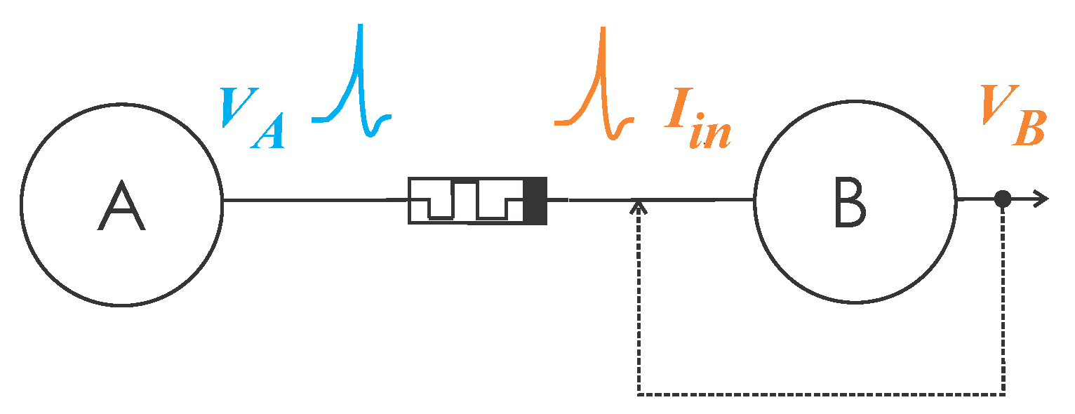
Equations 4, 5, presented in SubSection 2.2.1, model the change in tunnel resistance as a function of the time and the applied voltage to a memristor device. This model requires process-dependent parameters for a specific memristor device. Therefore, a change in the memristance, herein the tunnel resistance, corresponds to a change in the synaptic weight through its equivalent memristor conductance. The synaptic weight, modeled in Equation 8, on the other side, computes the change in the synaptic weight considering the time separation between the action potentials of two interconnected spiking neurons under certain predefined constant values. Consequently, using a SPICE memristor macromodel, presented in code block , allows us to closely simulate the STDP learning rule, expressed in 8. The STDP learning rule can be simulated in SPICE by simply plugging a memristor macromodel, like the one introduced in Seccion Section 2.2.1, between two spiking neurons circuit cells shown in Figure 2. Circuit cells have to be able to feed back their output to their input whenever a spike is produced. Doing so potentiates the synaptic strength (memristor conductance) if the pre-synaptic neuron fires before the post-synaptic neuron. It depreciates the synaptic strength if the pre-synaptic neuron fires after the post-synaptic neuron. The key point in a CMOS circuit synaptic implementation is to maintain the connection of the memristor terminals to the output potentials present in the pre-and-postsynaptic neurons to produce changes in the memristance as a function of the neuron spiking activity. In the next Subsection, we will explain the proposed circuit implementation to produce STDP learning.

2.4. Analog Leaky Integrate-and-Fire Functional Blocks and Control Signals

Numerous architectures for analog leaky-integrate-and-fire (LIF) neurons have been documented in the literature. The main component of such architectures is an integrator, responsible for receiving input spikes, integrating them over time, and producing an output spike once a certain voltage threshold v t h is attained. Various components, such as BJT transistors, silicon-controlled rectifiers [21], and floating-gate transistors [8] can be used as an integrator and trigger stage. In this work, we adopt the design proposed in [22] as a starting point. This design proposes a re-configurable architecture where the integrator can function as a buffer, thus giving the ability to deliver a higher output current to feed other neurons in a subsequent layer and to feed back its membrane potential to the right-side memristors terminals connected to its input of the antecedent layer, see Figure 2. Self-directed channel (SDC) memristors are utilized to implement the synaptic weights between neurons; these devices are already available and allow the implementation of proof of concept for this neural network on an analog system.
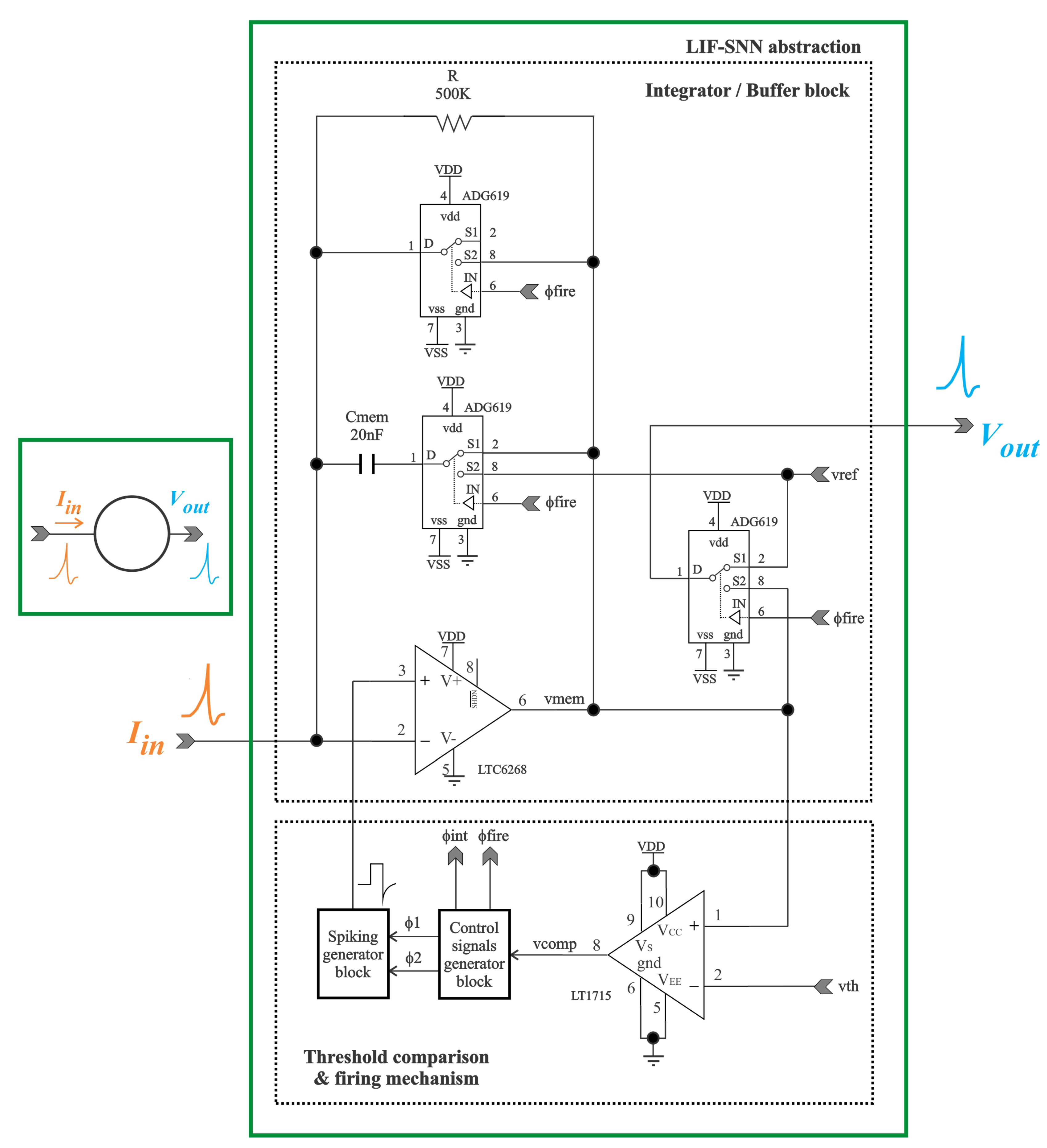
The block diagram of the LIF neuron proposed in [22] can be seen in Figure 3. This design employs an operational amplifier (opamp) that is initially configured as an integrator; once the integrated voltage reaches a threshold v t h , the voltage comparator triggers the generation of four control signals ( ϕ 1 , ϕ 2 , ϕ i n t , ϕ f i r e ). Two of these signals ϕ i n t and ϕ f i r e modify the state of the voltage-controlled switches that, in turn, reconfigure the opamp to act as a buffer. This buffer propagates a generated spiking signal, which is suited to drive the memristors in the synapses.
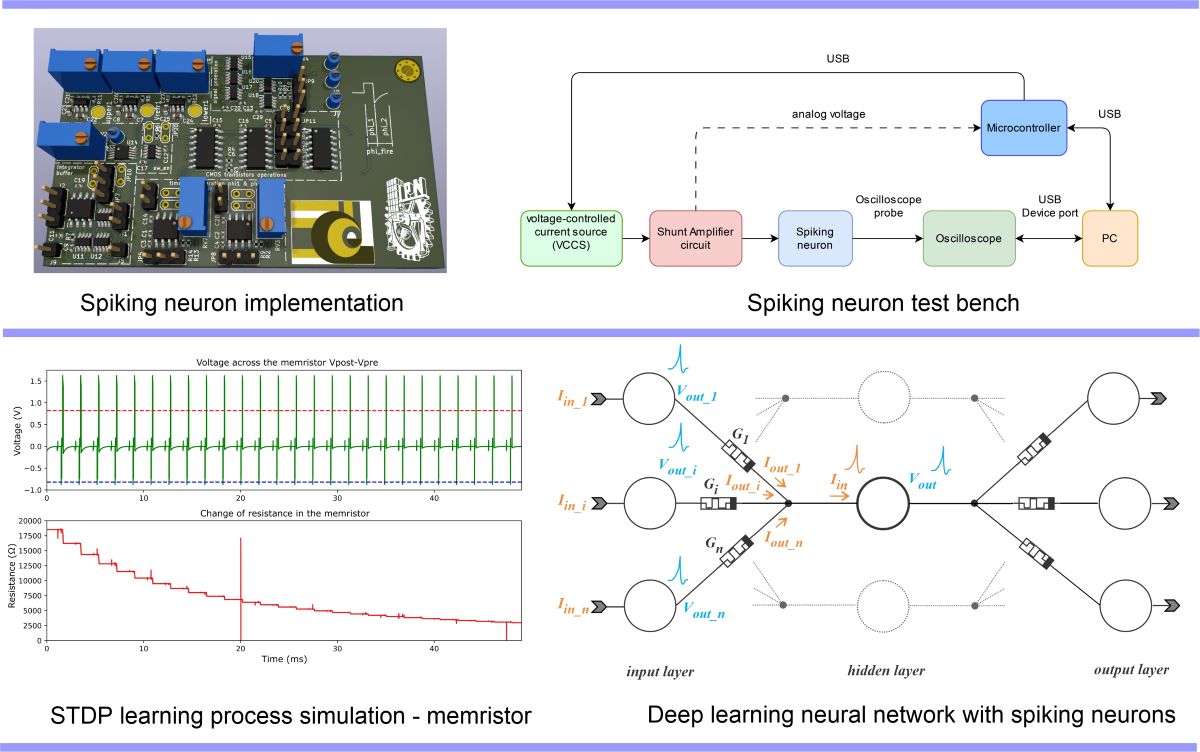
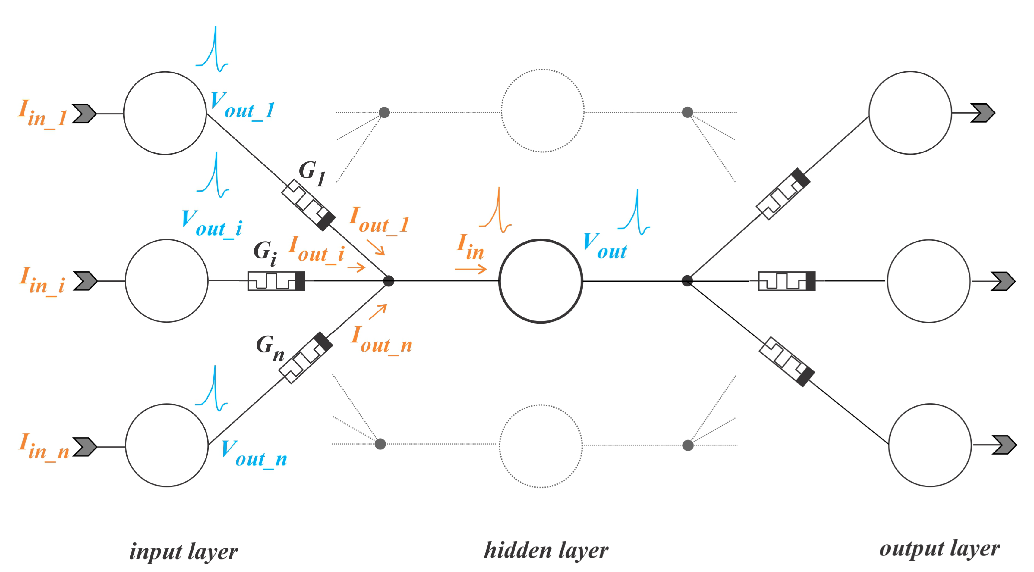
The design of the LIF neuron presented in Figure 3 and the memristive synapse it drives is quite important because these elements can be used as the starting building blocks for a much wider array of spiking neurons and synapses, essentially to implement power-efficient architectures for deep learning neural networks (DNN) in the analog domain, capable of being trained in-situ with the STDP learning rule. An outline for such a DNN abstraction is presented in Figure 4, where multiple layers of neurons are interconnected as fully or sparsely connected by memristive synapses.

2.4.1. Phase Control for Reconfiguration of the LIF Neuron

Figure 3 shows the main components of the analog spiking neuron circuit. These are an opamp to implement an integrator circuit, a comparator to compare the membrane potential, V m e m , with a predefined voltage threshold, V t h , a spiking generator circuit block, and a control signals generator block (CSGB). A capacitor and a resistance are also part of the proposal, reproducing the membrane capacitance and the leaky resistance present in the LIF neuron. Using switches implemented with transmission gates (TG), the LIF circuit changes its interconnections to behave like a leaky integrator during the integration phase and as a voltage buffer when the firing mechanism is activated when the membrane potential reaches V t h .
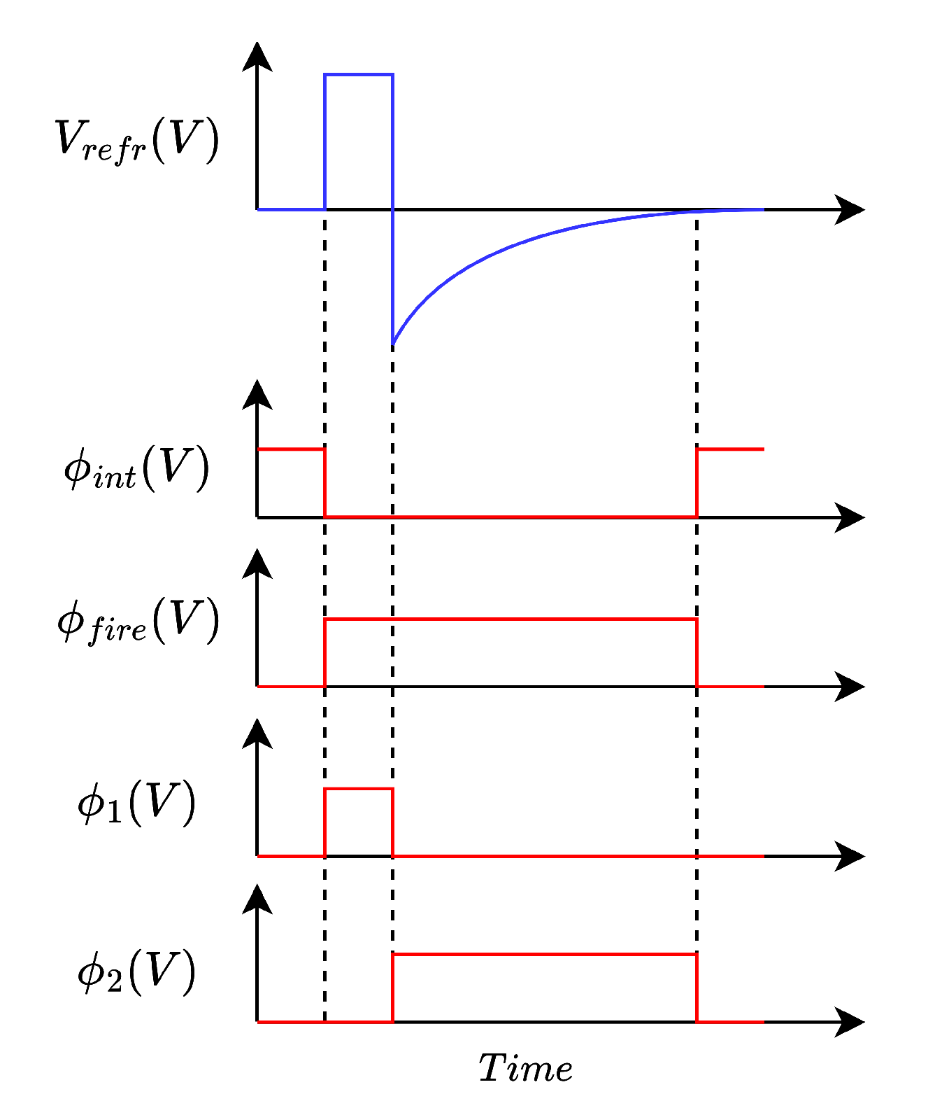
The state of the different TG is controlled through the use of the CSGB. The CSGB presented on [22] is only behaviorally described by the time diagram presented in Figure 5. The control signals ϕ 1 and ϕ 2 are reminiscent of the behavior of two mono-stable timers in series, in which the end of the first mono-stable timer ϕ 1 activates the second timer ϕ 2 . The ϕ f i r e signal represents the total time elapsed between both timers, and the ϕ i n t is the opposite of the ϕ f i r e signal.
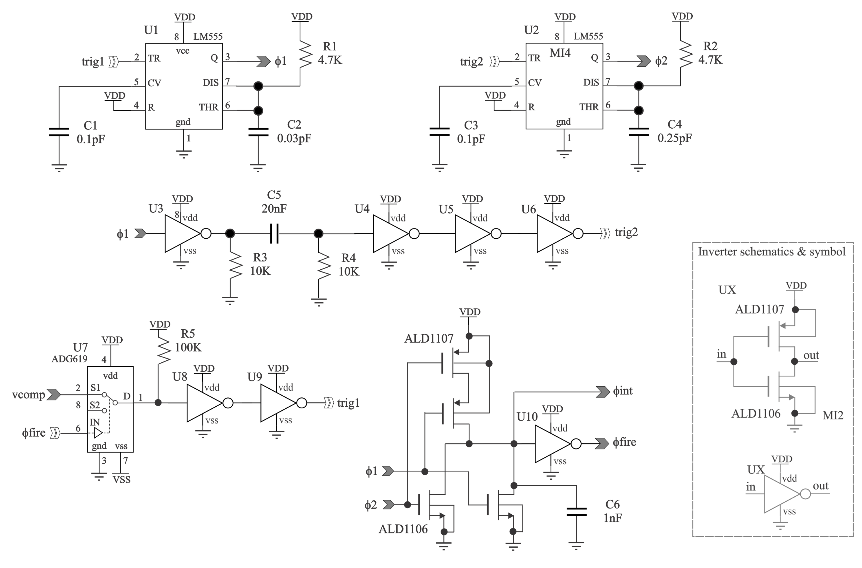
The proposed electrical circuit for the generation of the control signals ϕ 1 , ϕ 2 , ϕ i n t and ϕ f i r e is introduced in Figure 6, this circuit comprises two 555 timers configured as mono-stable timers. The first timer is triggered by the output signal of the LT1715 CMOS comparator, shown in Figure 3; this signal is reshaped using two CMOS inverters. The output of the first timer ( ϕ 1 ) is then fetched through a CMOS inverter and a resistor-capacitor (RC) circuit, which in turn eliminates all constant signals and only reacts with any change in voltage, functioning as an impulse function. This signal is reshaped and fetched to the second timer, producing the signal ϕ 2 at the output of this second timer. Signal ϕ f i r e can be seen as the logic XOR operation of the signals ϕ 1 and ϕ 2 . The implementation of a logic XOR gate requires only 4 CMOS transistors. By inverting the ϕ f i r e signal, we can obtain the ϕ i n t signal.

2.5. Electrical Characteristics of the Block Components of the LIF Neuron

A physical implementation of a LIF neuron requires the utilization of different commercial components, these components must be chosen under the specifications outlined in [22] and the availability of simulation models for LTSpice, the process is elaborated in the subsequent sections.

2.5.1. Integration/Buffer and Comparator Module

In Table 1, the characteristics required in the integrator/buffer module considered in [22] are presented alongside the characteristics of the selected components. Considering the characteristics of the commercially available devices, the search is narrowed down to two components, the ADA4680, and the ALTC6268. Although the ADA4680 has greater rise and fall speed, it does so with a lower output voltage of 2v peak to peak, in comparison with the slower LTC6268 that can output a voltage between 0.5 to 4.5 volts, given that the voltage required to drive the memristors is above 2 volts, the ADA4680 would not be able to drive these devices, taking in consideration this the LTC6268 is selected.
The comparator has a single design parameter, a fast transient response that can detect pulses with a time width of 500 ns. Any comparator with a propagation delay (which is the time it takes to propagate an input signal to the output) lower of 500 ns would be suitable for this application, the LT1714 comparator has a propagation delay of 4.4 ns is selected due to a low cost, and ease of manufacturing.

2.5.2. Selection of Transmission Gates Modules

As discussed in the SubSection 2.4, the opamp circuit that works as an integrator or buffer is reconfigured using TG devices. A TG behaves as a voltage-controlled switch and modifies the operation of the opamp-based circuit. An ideal CMOS switch exhibits zero resistance when turned on and infinite resistance when turned off, but these ideal specifications are not realistic in practice. Table 2 shows the characteristics of the proposed TG. The ADG619 has a wider supply range while in dual mode, a low propagation delay with a higher voltage on the logic input, a low on-resistance (the total resistance of the switch while closed) [25] and an overall lower on-resistance flatness (which is the variation of the on-resistance during the entire voltage excursion).

2.5.3. Spiking Generator Block Design

The spiking generator block produces the neuron’s spike waveform, which will be fed the positive differential input of the opamp circuit when it operates as a buffer and drives the memristors. During the leaky integration phase, it supplies a reference voltage, V r e f . The waveform is shaped by four control signals ϕ 1 , ϕ 2 , ϕ i n t , ϕ f i r e shown in Figure 5 in a time diagram. Signal ϕ 1 controls the period of the active spike; this time is utilized in the synaptic weight adjustment. Signal ϕ 2 controls the absolute refractory period of the neuron, which is the period of time when the neuron ignores all incoming input impulses; this phenomenon naturally occurs on biological neurons and avoids an over-stimulation of neurons. Signal ϕ f i r e represents the time at which the neuron is firing an impulse, and ϕ i n t the time at which the neuron is integrating input impulses.
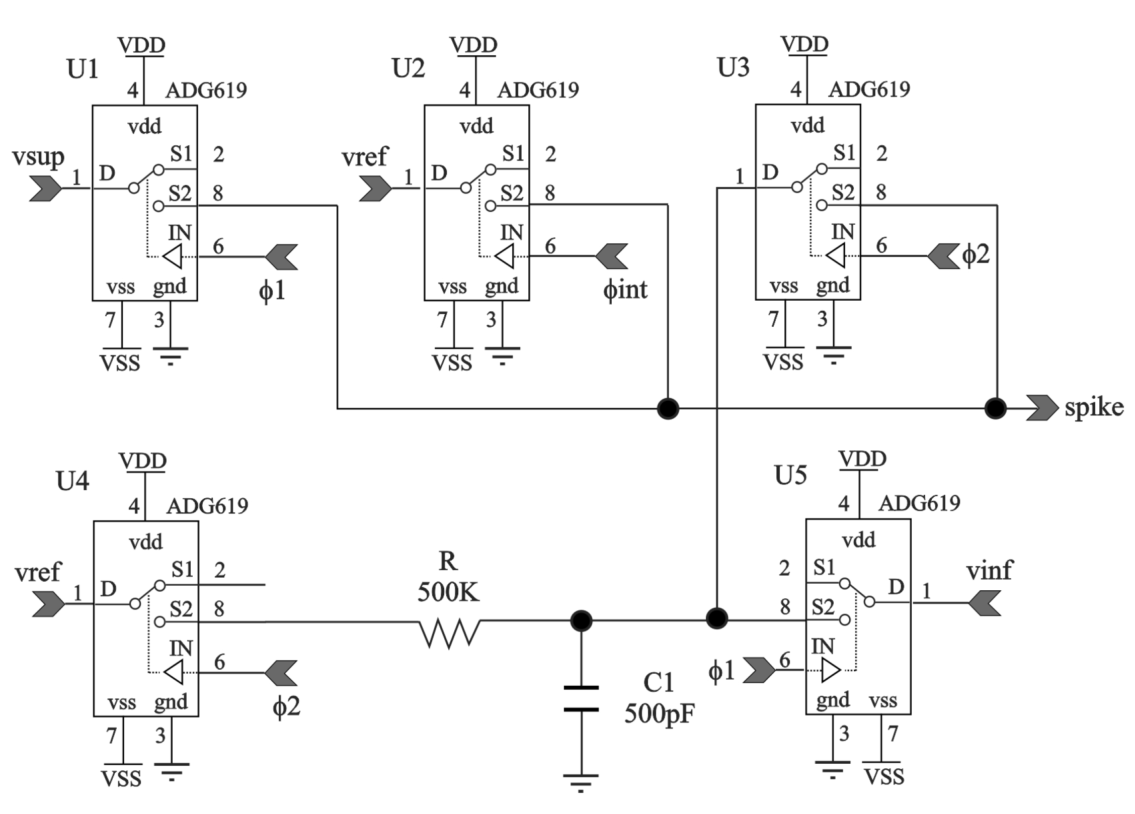
Figure 7 shows the proposed electrical circuit implementation for the spiking generation module. This module uses five TG to generate the desired signal output shape. The RC circuit incorporated in this proposal determines the relaxation time of the neuron. The values of 500 K Ω resistor and 500 p F capacitor are selected for two main reasons:
  • The commercial memristors by Knowm exhibit the greatest change in memristance at a low frequency (1Hz) and the smallest change at high frequency (1KHz) [29].
  • A total relaxation time of 1.25ms is within the absolute refractory period of mammal neurons, where neurons cannot generate new output spikes [30] contributing to sparse computing with low power.

3. Results

This section introduces the electrical simulations and measurements for the implemented LIF neuron prototype. The tests were conducted to obtain the tuning curve as a neuron figure of merit and the comparison between the theoretical STDP learning process of living organisms modeled by equation 7 and the STDP produced with two LIF neuron circuit cells linked with the Vourkas memristor macromodel in code block .

3.1. Electrical Simulation of the LIF Neuron

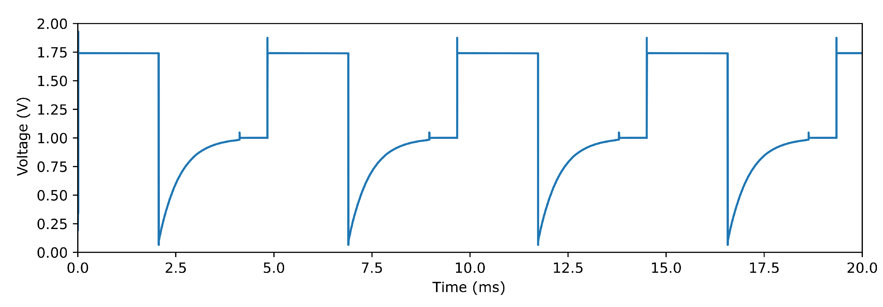
The electrical simulation of the neuron was conducted in the simulator LTSpice, with a constant input current of 5 μ A. With this input stimulus, the LIF neuron generates the output spikes shown in Figure 8. The subsequent step for the characterization of the LIF neuron is the acquisition of the tuning curve. The tuning curve is the response of any sensory neuron to external stimuli and the behavior it exhibits [31].
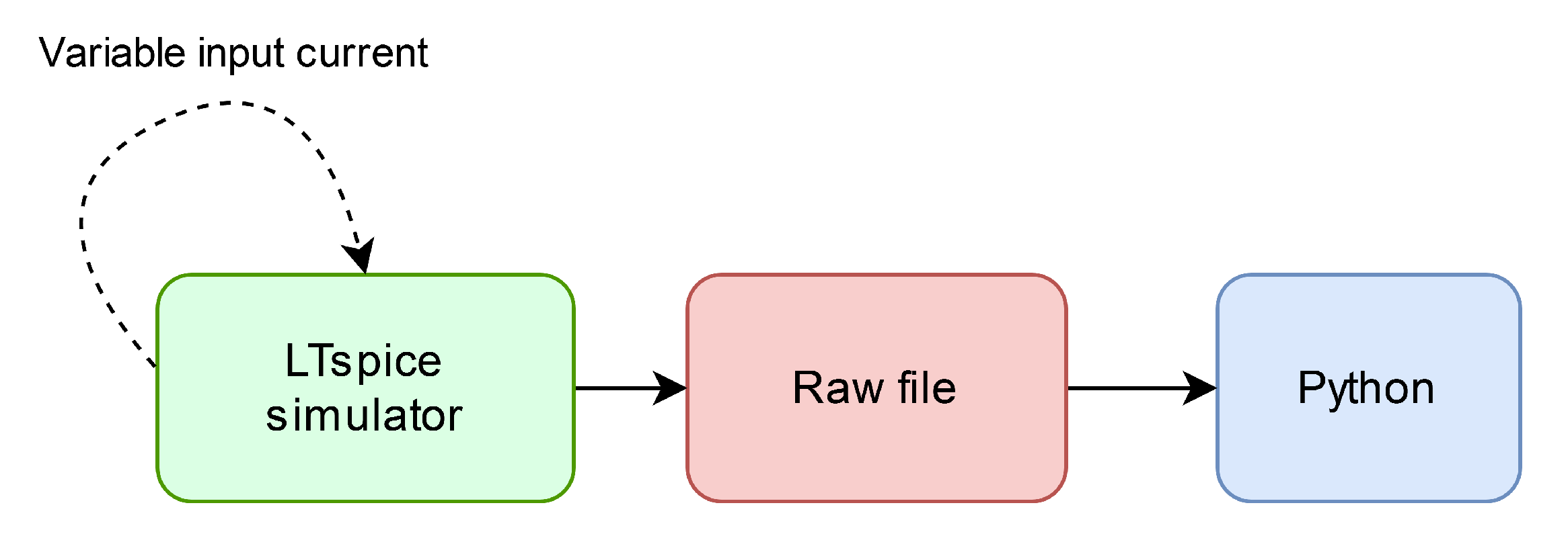
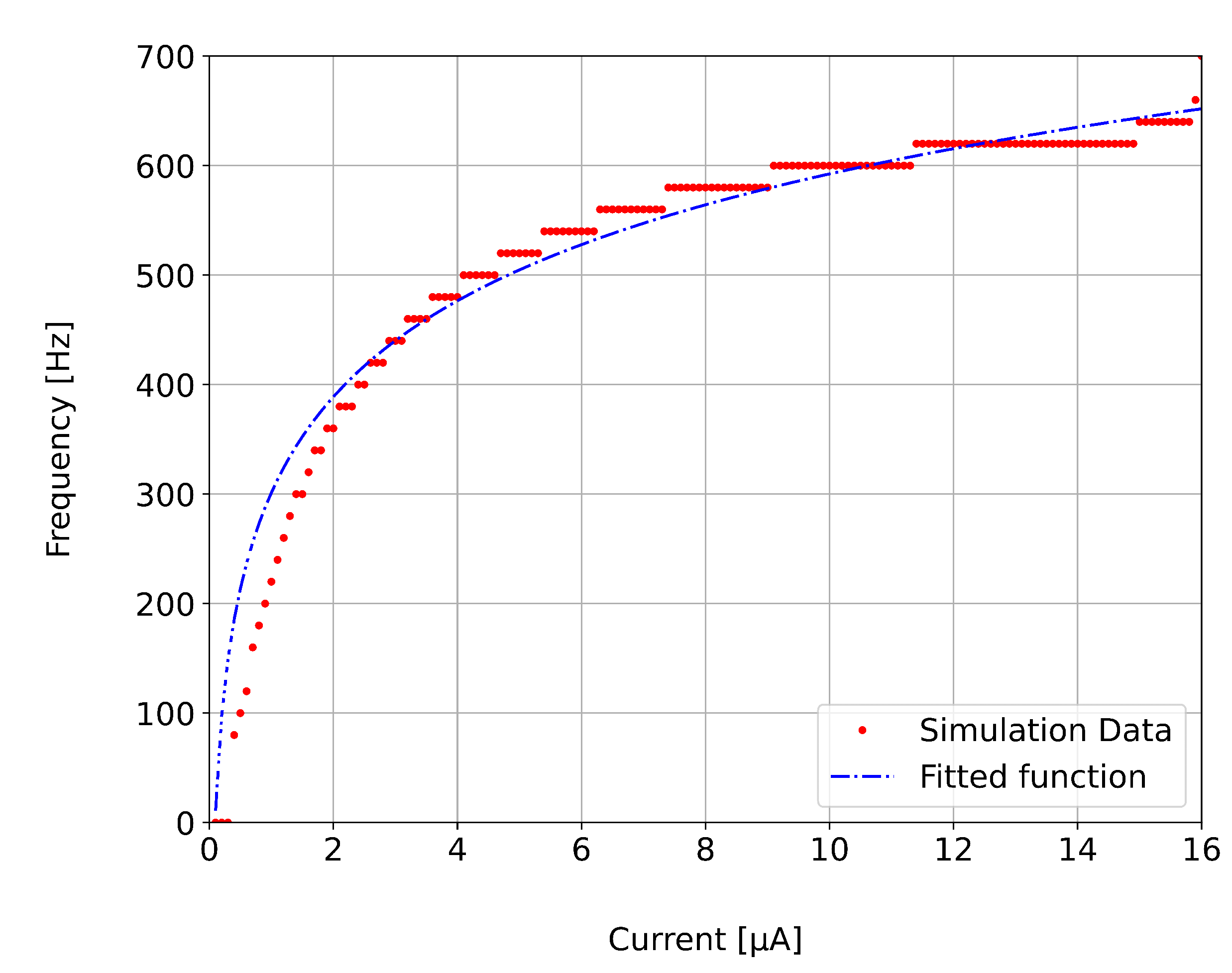
Figure 9 illustrates the methodology utilized for the neuron characterization. The test bench is configured to create a series of simulations, in each simulation a current source that acts as the neuron’s input, changes it’s value. The current source starts with a value of 0 μ A and reaches a stop value of 16 μ A ; the current source increases by 0.1 μ A , and in each simulation, the generated signals at the neuron’s output are stored in a RAW file. Subsequently, this RAW file is parsed to Python, where the data is extracted, analyzed, and used to calculate the frequency of the output spikes. This information is then utilized to generate a tuning curve, which can be seen in red on Figure 10. The neuron’s behavior can be approximated by the equation 9, which is calculated with a least square regression algorithm.
f ( x ) = 126.5 × l n x 0.09247

3.2. Hardware Implementation of the LIF Neuron

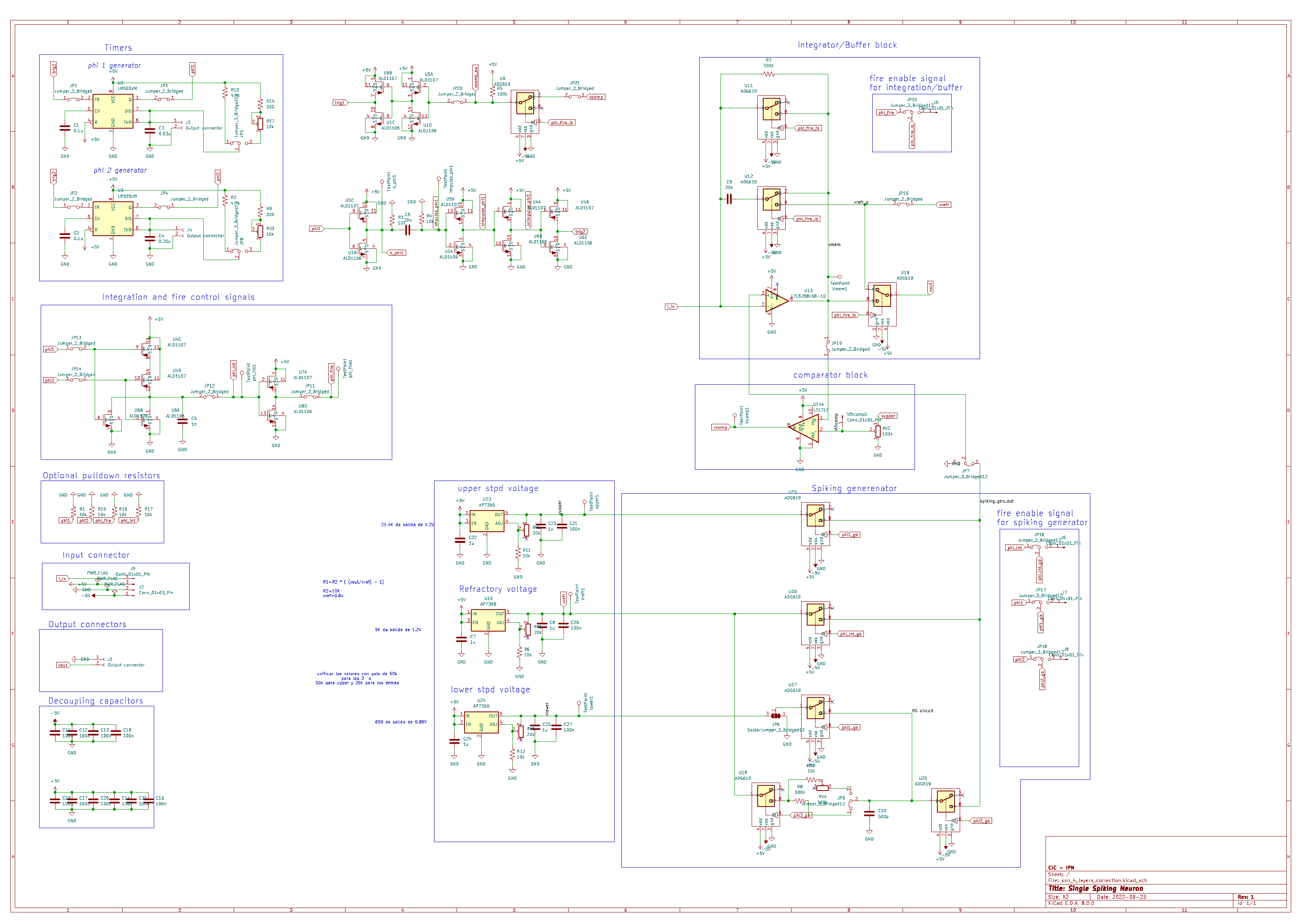
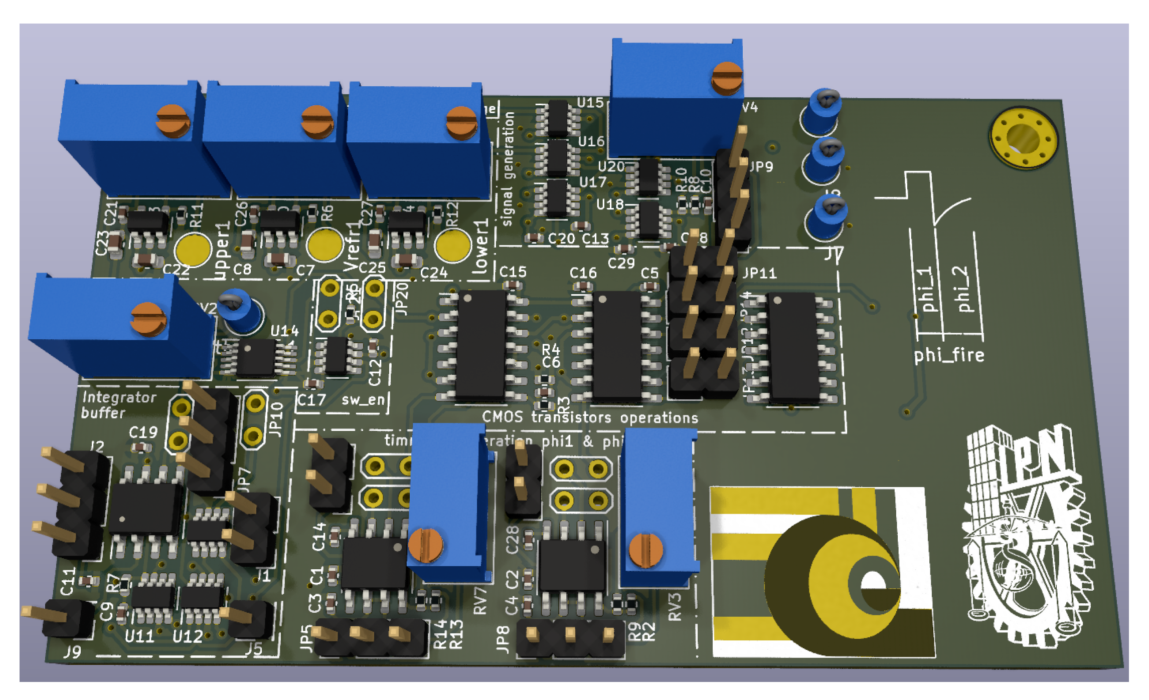
Appendix 19 contains the complete schematic used to design a printed circuit board (PCB) for the LIF neuron. The PCB design shows the commercial components used for the neuron prototype, testing points, and trimmers that allow for tuning of neuron parameters, such as relaxation time, control signal timing, and V t h , among others. Figure 11 shows a 3D rendering of the PCB.
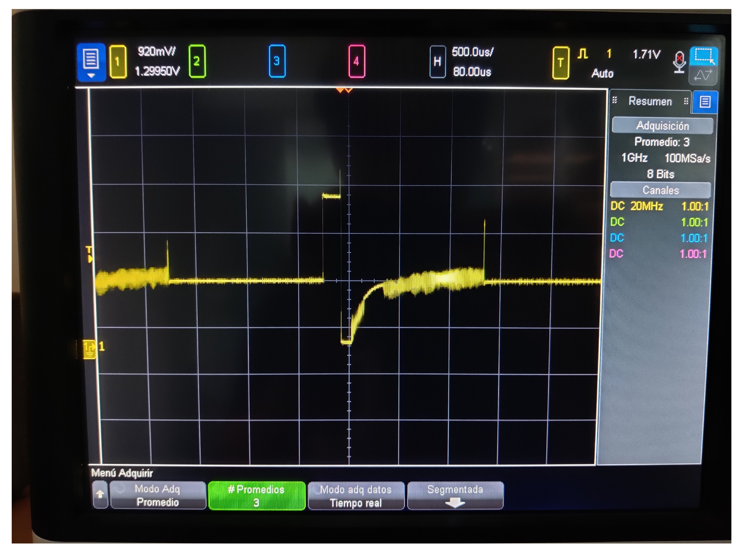
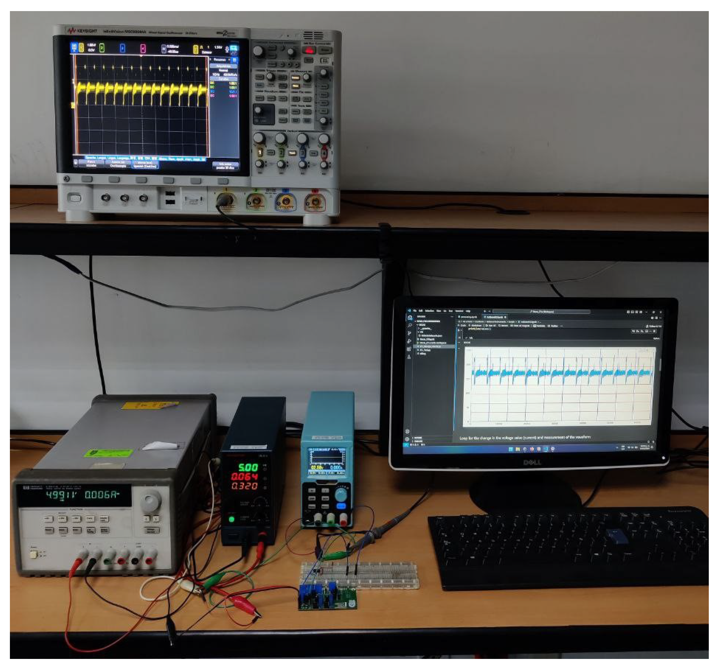
The assembled LIF neuron prototype shown in Figure 11 was tested with a constant neuron’s input current of 4 μ A . The neuron response is introduced in Figure 12. The experimental testbench for the LIF neuron prototype is shown in Figure 13.

3.2.1. Methodology for the Characterization of the Physical LIF Neuron

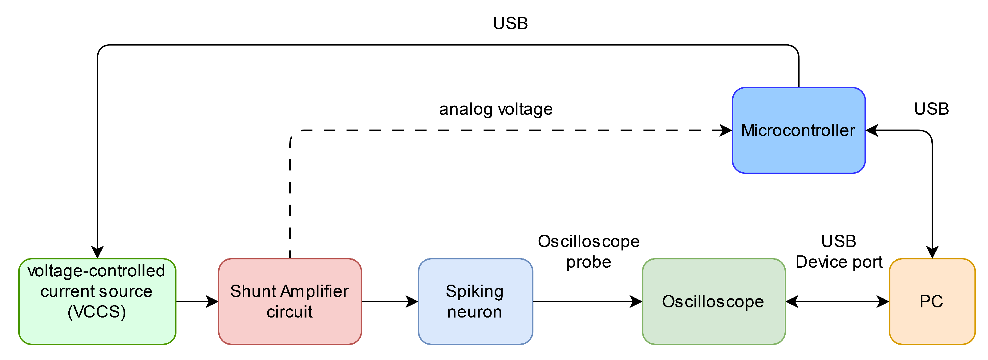
The methodology described in Figure 9 for characterizing the LIF neuron relies on the simulator being able to modify the input current source of the neuron and store the values generated at the output of the neuron. To achieve the same result in the implementation of the neuron, the test equipment needs to modify the input current, read the output spikes from the neuron, and store the acquired data, Figure 14 outlines the methodology utilized to achieve this result. A voltage-controlled current source (VCSS) is connected in series with a shunt amplifier; this amplifier monitors the current supplied by the VCSS and modifies the value if necessary; the output current will be the input of the spiking neuron. The output spikes are monitored with an oscilloscope, which is controlled by a PC with the use of a Virtual Instrument [32]; this communication protocol allows the interaction with the oscilloscope and retrieves data automatically; the VCSS is controlled by a microcontroller, which also monitors the current supplied to the spiking neuron. The data points gathered by the oscilloscope are stored on the PC, which will be used to calculate the frequency of the output spikes.
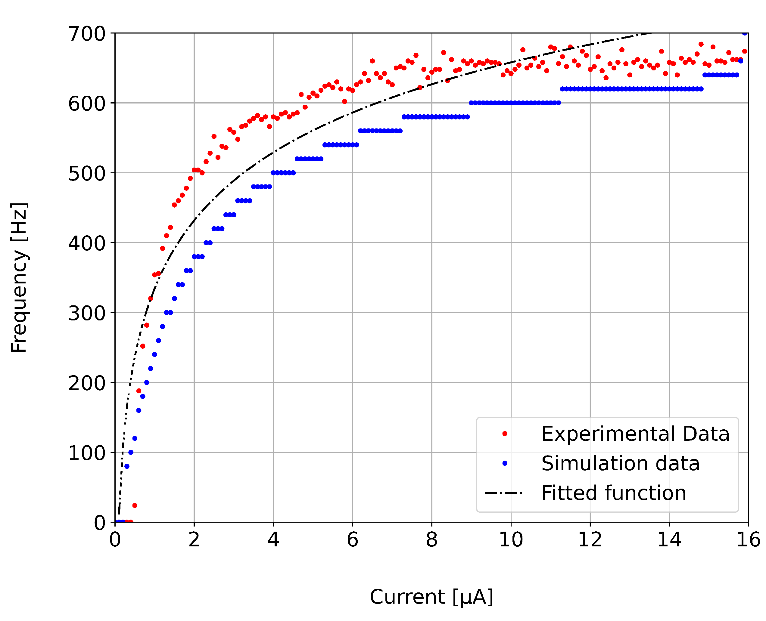
Figure 15 shows the electrical response of the LIF neuron prototype. The data points obtained from the physical implementation closely follow the behavior of the LIF neuron simulation, with a shift in the frequency response; the data can be approximated with the equation 10, which is also calculated with a least square regression and in accordance with the equation 9 utilized for the simulated data points with a different gain value.
f ( x ) = 140.5 × l n x 0.09247

3.3. Simulation of the Synaptic Weight Adjustment of a Memristive Synapse

The testbench used to simulate the synaptic weight adjustment with the aid of the memristor’s macromodels in code block is presented in the following sections.

3.3.1. Long-Term Potentiation On Memristive Synapse

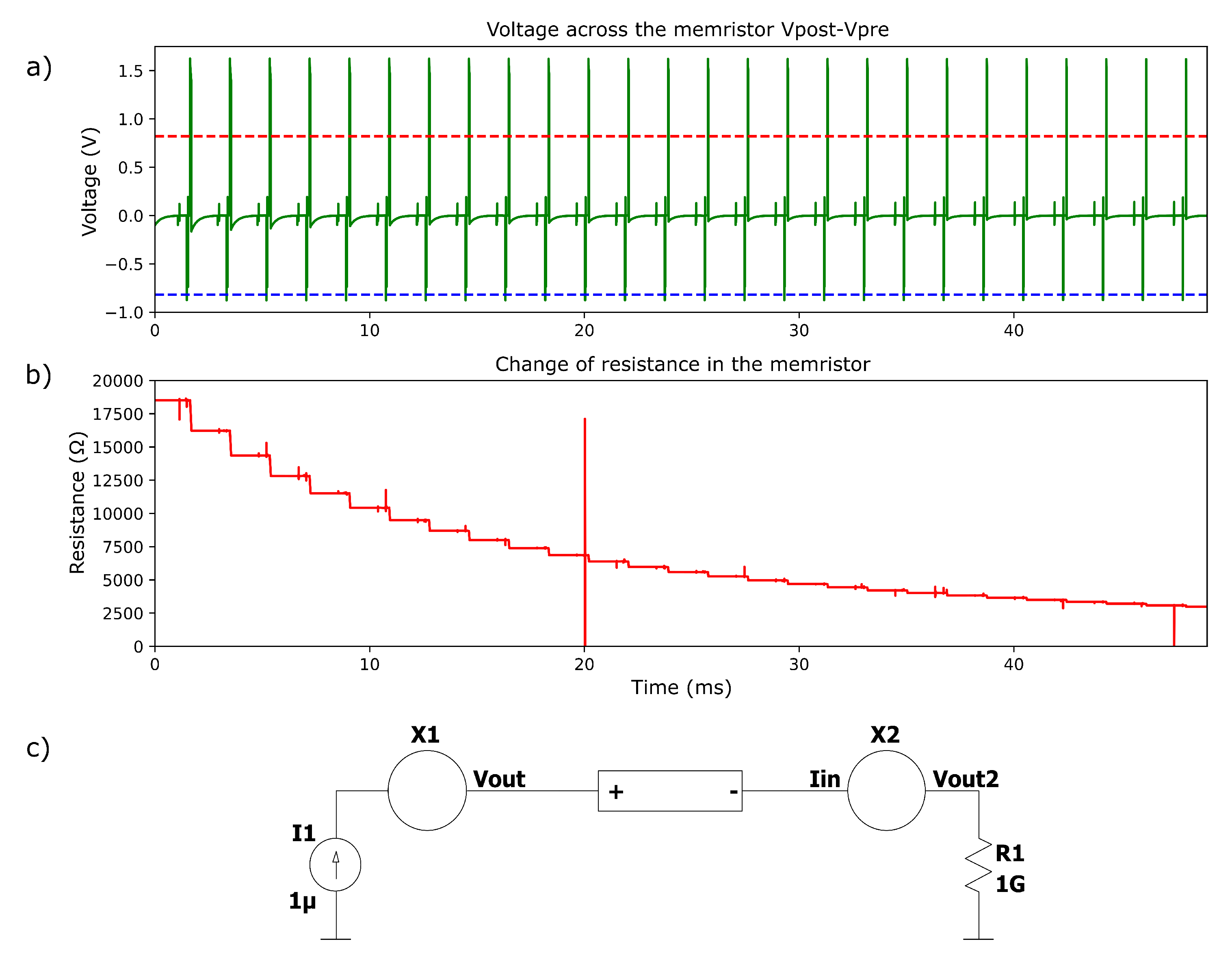
Figure 16 shows the potentiation response of a memristive synapse placed between two LIF neurons. As it was expected, the presynaptic neuron X 1 , fires first due to the constant current input applied I 1 ; see Figure 16c. It is observed that, after several spikes produced by the X 1 LIF neuron, the postsynaptic LIF neuron X 2 starts spiking at a slower rate. Therefore, the convolution between the pre-synaptic and post-synaptic spikes surpasses the positive voltage memristor threshold, then potentiating the synapse. The voltage across the memristor is shown in Figure 16a.

3.3.2. Spike-tIming-Dependent Plasticity (STDP) Process on a Memristive Synapse

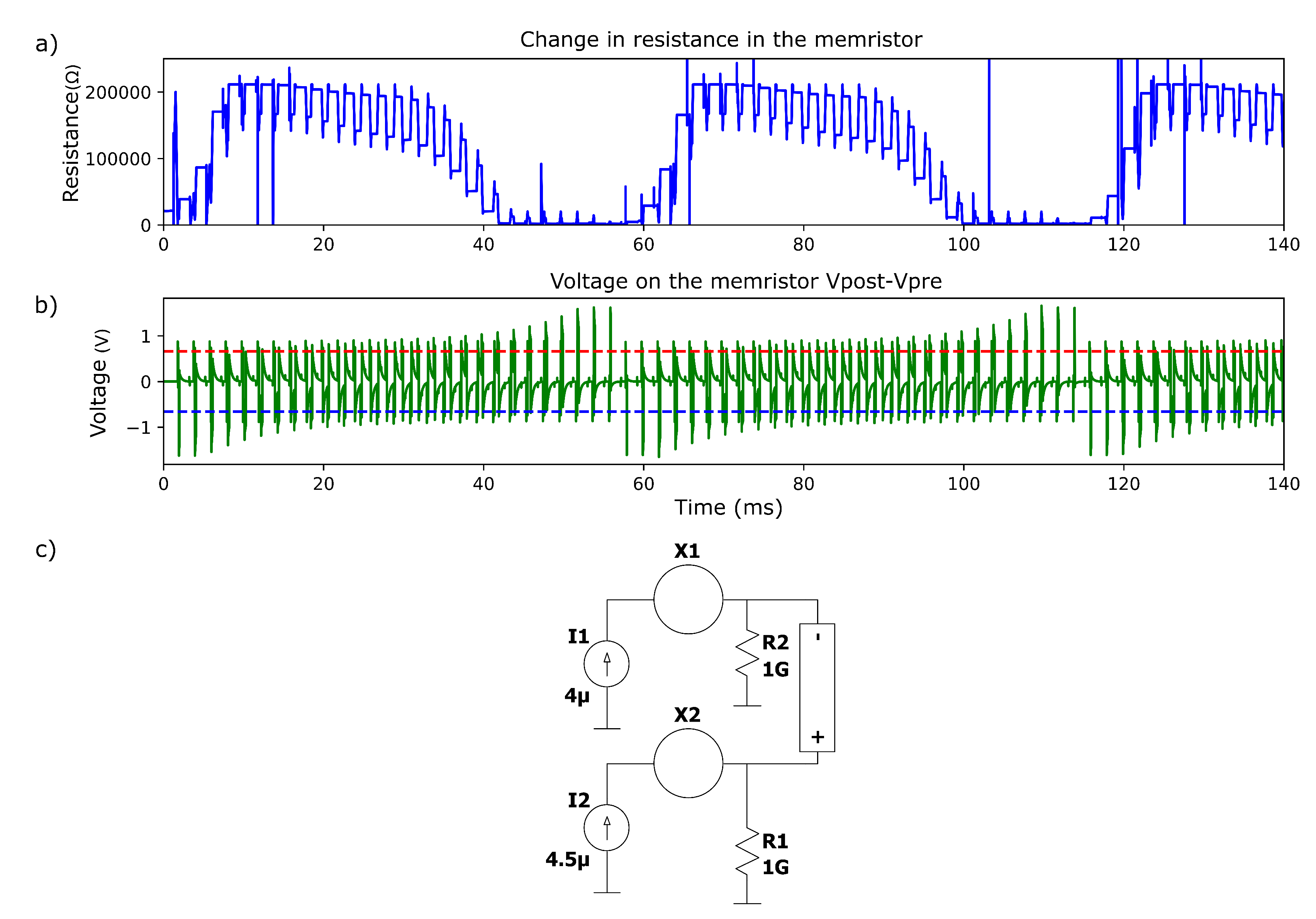
Figure 17c shows the testbench used to induce a periodic cycle of potentiation and depression on a memristive synapse. Based on the STDP process, the memristor reaches the highest (positive and negative) value of resistance change, when the time windows between the pre-synaptic and post-synaptic spikes reach a minimum value, see Figure 17b. If the time window reaches zero or a value close to zero, the change in the synaptic weight decreases exponentially; this is due to a physical constraint in memristive devices. In this testbench a memristor is placed at the output of two neurons with different firing frequencies; the difference in the output spike frequency results in a cycle of potentiation and depression of the synapses, as shown in green in Figure 17a.
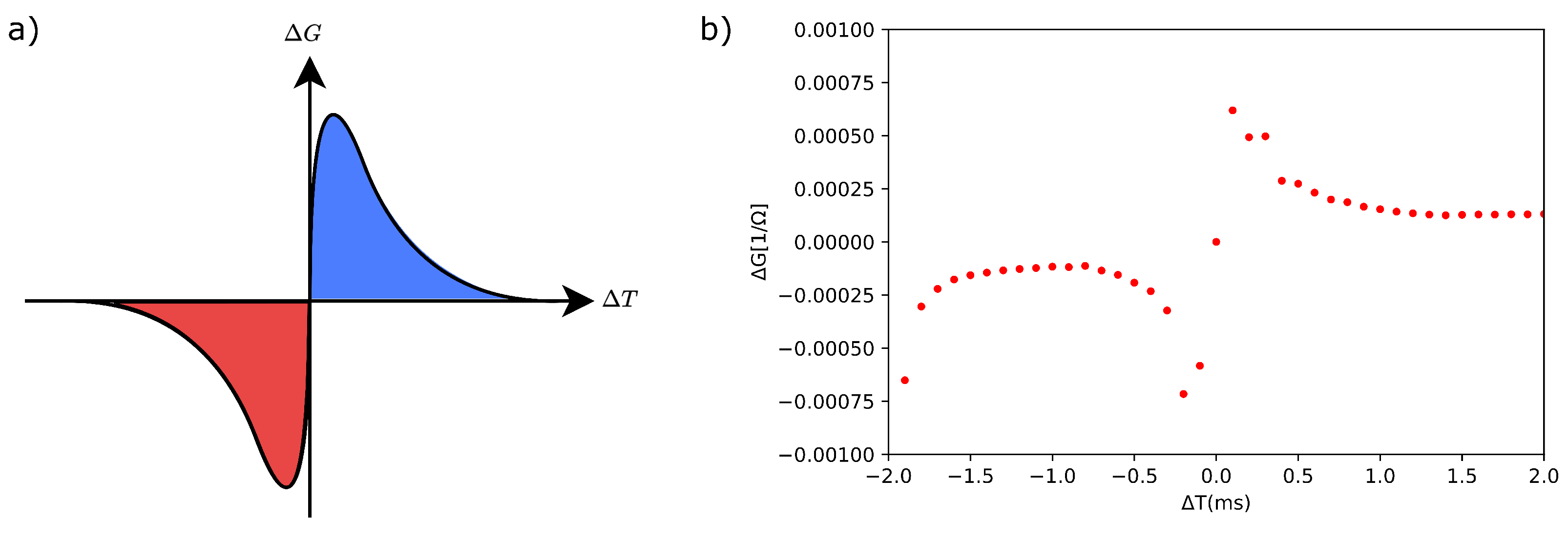
Figure 18(b) shows the resulting synaptic weight adjustment curve as a function of Δ t . The obtained curve with the proposed LIF neuron circuit is in agreement with the typical curve present in living organisms [33], see Figure 18(a). The synaptic weight adjustment increases as the Δ t decreases. When this Δ t values reaches zero, the weight decreases exponentially, as it implies the generation of very sharp spikes, exceeding any positive or negative memristor’s voltage threshold. However, the internal memristor dynamics is unable to produce a significant change in the memristance due to that the oxygen drift velocity mechanism in, i.e., TiO2 dielectric films, is much slower than the brevity of time the electric field is present between the terminals of the memristor. In this test, the maximum weight adjustment is around 750 micro Siemens.

4. Conclusions

This article presents the design and implementation of a leaky integrate-and-fire neuron prototyped with commercial components for neuromorphic computing. The LIF neuron circuit simulations and the spiking production’s electrical measurements showed a small deviation in the tuning curve behavior. This is due mainly to the tolerance values in each electronic component soldered on the PCB. Despite these variations, the neuron LIF realization on PCB retains the overall behavior obtained in the simulation. The rate of change of the memristance in simulation for the artificial synapse element motivates us to explore the interconnection of the neuron LIF cells in PCB to form a spiking neural network for neuromorphic computing experimentation.
The implementation has a total power consumption of around 350mW, from which 190mW corresponds to the three linear voltage regulators utilized for the reference signals of the spiking generator block; a single neuron is capable of driving 4500 neurons with memristive synapses, considering that each neuron would consume a maximum of 20 μ A.
The method presented for characterizing the spiking neuron can also be used to measure and create an accurate memristive synapse model. This synapse model can be implemented in Python to develop deep-learning models that can be integrated into circuits. Using spiking neurons, circuit cells, and memristive synapses allow for sparse system operation. This opens up the possibility of implementing new low-power, low-latency deep neural network computing hardware platforms with robust operation that can be further developed for integrated circuits with applications in Edge and IoT devices.

4.1. Future Work

In our future work, our goal is to take the tuning curve of the physical neuron, combine it with the equation that describes the behavior of the LIF neuron, and program it in Python to create simulations that mimic the physical prototype. We will then instantiate it multiple times to develop a deep learning architecture simulation framework. Doing this will enable us to experiment by exploring information encoding and decoding schemes, solving pattern recognition problems, and controlling robotics.

Author Contributions

Conceptualization, R.R; Methodology, R.R.; Software, O.I.; Validation, H.M.; Formal analysis, J.S.; Investigation, R.R, V.P. and O.I; Resources, V.P.; Data curation, R.R; Writing – original draft, R.R; Writing – review & editing, V.P; Visualization, E.R; Supervision, H.M. All authors have read and agreed to the published version of the manuscript.

Funding

The authors are thankful for the financial support of the projects to the Secretaría de Investigación y Posgrado del Instituto Politécnico Nacional with grant numbers 20232264, 20242280, 20231622, 20240956, 20232570 and 20242742, as well as the support from Comisión de Operación y Fomento de Actividades Académicas and Consejo Nacional de Humanidades Ciencia y Tecnología (CONAHCYT).

Institutional Review Board Statement

Not applicable.

Informed Consent Statement

Not applicable.

Data Availability Statement

All of the scripts used in this article are available on the following Github page: https://github.com/RoyceRichmond/AnalogSNN_on_Hardware (accessed on 20 April 2024).

Conflicts of Interest

The authors declare no conflicts of interest.

Abbreviations

The following abbreviations are used in this manuscript:
Opamp Operational amplifier
LIF Leaky integrate-and-fire
STDP Spike timing-dependent plasticity
LTP Long-term potentiation
LTD long-term depression
Figure 19. Schematic diagram of the proposed neuron LIF design.
Preprints 107862 g019

References

  1. Brown, T.B.; Mann, B.; Ryder, N.; Subbiah, M.; Kaplan, J.; Dhariwal, P.; Neelakantan, A.; Shyam, P.; Sastry, G.; Askell, A.; Agarwal, S.; Herbert-Voss, A.; Krueger, G.; Henighan, T.; Child, R.; Ramesh, A.; Ziegler, D.M.; Wu, J.; Winter, C.; Hesse, C.; Chen, M.; Sigler, E.; Litwin, M.; Gray, S.; Chess, B.; Clark, J.; Berner, C.; McCandlish, S.; Radford, A.; Sutskever, I.; Amodei, D. Language Models are Few-Shot Learners. CoRR 2020 abs/2005.14165 [2005.14165].
  2. Ramesh, A.; Dhariwal, P.; Nichol, A.; Chu, C.; Chen, M. Hierarchical Text-Conditional Image Generation with CLIP Latents, 2022, [arXiv:cs.CV/2204.06125].
  3. Luccioni, A.S.; Viguier, S.; Ligozat, A.L. Estimating the Carbon Footprint of BLOOM, a 176B Parameter Language Model, 2022, [arXiv:cs.LG/2211.02001].
  4. Analog VLSI Implementation of Neural Systems; Springer US, 1989. [CrossRef]
  5. Maass, W. Networks of spiking neurons: The third generation of neural network models. Neural Networks 1997, 10, 1659–1671. [Google Scholar] [CrossRef]
  6. Costandi, M. Neuroplasticity; The MIT Press Essential Knowledge series; MIT Press: London, England, 2016. [Google Scholar]
  7. Chakraborty, I.; Jaiswal, A.; Saha, A.K.; Gupta, S.K.; Roy, K. Pathways to efficient neuromorphic computing with non-volatile memory technologies. Applied Physics Reviews 2020, 7[https://pubs.aip.org/aip/apr/article-pdf/doi/10.1063/1.5113536/14576835/021308_1_online.pdf]. 021308,. [CrossRef]
  8. Kornijcuk, V.; Lim, H.; Seok, J.Y.; Kim, G.; Kim, S.K.; Kim, I.; Choi, B.J.; Jeong, D.S. Leaky Integrate-and-Fire Neuron Circuit Based on Floating-Gate Integrator. Frontiers in Neuroscience 2016, 10. [Google Scholar] [CrossRef] [PubMed]
  9. Linares-Barranco, B.; Serrano-Gotarredona, T.; Camuñas-Mesa, L.; Perez-Carrasco, J.; Zamarreño-Ramos, C.; Masquelier, T. On Spike-Timing-Dependent-Plasticity, Memristive Devices, and Building a Self-Learning Visual Cortex. Frontiers in Neuroscience 2011, 5. [Google Scholar] [CrossRef] [PubMed]
  10. Chua, L. Memristor-The missing circuit element. IEEE Transactions on Circuit Theory 1971, 18, 507–519. [Google Scholar] [CrossRef]
  11. Nature Electronics 2023, 6, 463–463. [CrossRef]
  12. Hodgkin, A.L.; Huxley, A.F. A quantitative description of membrane current and its application to conduction and excitation in nerve. The Journal of Physiology 1952, 117, 500–544. [Google Scholar] [CrossRef] [PubMed]
  13. Gerstner, W.; Kistler, W.M.; Naud, R.; Paninski, L. Neuronal Dynamics: From Single Neurons to Networks and Models of Cognition; Cambridge University Press, 2014. [CrossRef]
  14. Strukov, D.B.; Snider, G.S.; Stewart, D.R.; Williams, R.S. The missing memristor found. Nature 2008, 453, 80–83. [Google Scholar] [CrossRef] [PubMed]
  15. Joglekar, Y.N.; Wolf, S.J. The elusive memristor: properties of basic electrical circuits. European Journal of Physics 2009, 30, 661. [Google Scholar] [CrossRef]
  16. Vourkas, I.; Sirakoulis, G.C. Memristor-Based Nanoelectronic Computing Circuits and Architectures; Springer International Publishing, 2016. [CrossRef]
  17. Hebb, D.O. The organization of behavior; Psychology Press: Philadelphia, PA, 2002. [Google Scholar]
  18. Dayan, P.; Abbott, L.F. Theoretical neuroscience; Computational neuroscience, MIT Press: London, England, 2001. [Google Scholar]
  19. Caporale, N.; Dan, Y. Spike Timing–Dependent Plasticity: A Hebbian Learning Rule. Annual Review of Neuroscience 2008, 31, 25–46. [Google Scholar] [CrossRef] [PubMed]
  20. Rastogi, M.; Lu, S.; Islam, N.; Sengupta, A. On the Self-Repair Role of Astrocytes in STDP Enabled Unsupervised SNNs. Frontiers in Neuroscience 2021, 14. [Google Scholar] [CrossRef] [PubMed]
  21. Rozenberg, M.J.; Schneegans, O.; Stoliar, P. An ultra-compact leaky-integrate-and-fire model for building spiking neural networks. Scientific Reports 2019, 9. [Google Scholar] [CrossRef] [PubMed]
  22. Wu, X.; Saxena, V.; Zhu, K.; Balagopal, S. A CMOS Spiking Neuron for Brain-Inspired Neural Networks With Resistive Synapses and In Situ Learning. IEEE Transactions on Circuits and Systems II: Express Briefs 2015, 62, 1088–1092. [Google Scholar] [CrossRef]
  23. Analog Devices. 500MHz Ultra-Low Bias Current FET Input Op Amp, 2017.
  24. Analog Devices. High Speed, Low Cost,Op Amp, 2006. Rev. 0.
  25. Banerjee, W.; Nikam, R.D.; Hwang, H. Prospect and challenges of analog switching for neuromorphic hardware. Applied Physics Letters 2022, 120. [Google Scholar] [CrossRef]
  26. Analog Devices. CMOS, ±5 V/+5 V,4 Ω, Single SPDT Switches, 2011. Rev. C.
  27. Analog Devices. CMOS, 2.5 Ω Low Voltage,Triple/Quad SPDT Switches, 2001. Rev. B.
  28. Analog Devices. 2.5 Ω, 1.8 V to 5.5 V, ±2.5 V Triple/Quad SPDT Switches in Chip Scale Packages, 2015. Rev. C.
  29. Knowm. Memristors to Machine Intelligence. Available: https://knowm.org/.
  30. Maida, A. Chapter 2 - Cognitive Computing and Neural Networks: Reverse Engineering the Brain. In Cognitive Computing: Theory and Applications; Gudivada, V.N.; Raghavan, V.V.; Govindaraju, V.; Rao, C., Eds.; Elsevier, 2016; Vol. 35, Handbook of Statistics, pp. 39–78. [CrossRef]
  31. Butts, D.A.; Goldman, M.S. Tuning Curves, Neuronal Variability, and Sensory Coding. PLoS Biology 2006, 4, e92. [Google Scholar] [CrossRef]
  32. Keysight. InfiniiVision X-Series Oscilloscope LabVIEW Instrument Drivers. Available: https://www.keysight.com/us/en/lib/software-detail/driver/infiniivision-xseries-oscilloscope-labview-instrument-drivers-2862255.html.
  33. Stoliar, P.; Yamada, H.; Toyosaki, Y.; Sawa, A. Spike-shape dependence of the spike-timing dependent synaptic plasticity in ferroelectric-tunnel-junction synapses. Scientific Reports 2019, 9. [Google Scholar] [CrossRef] [PubMed]
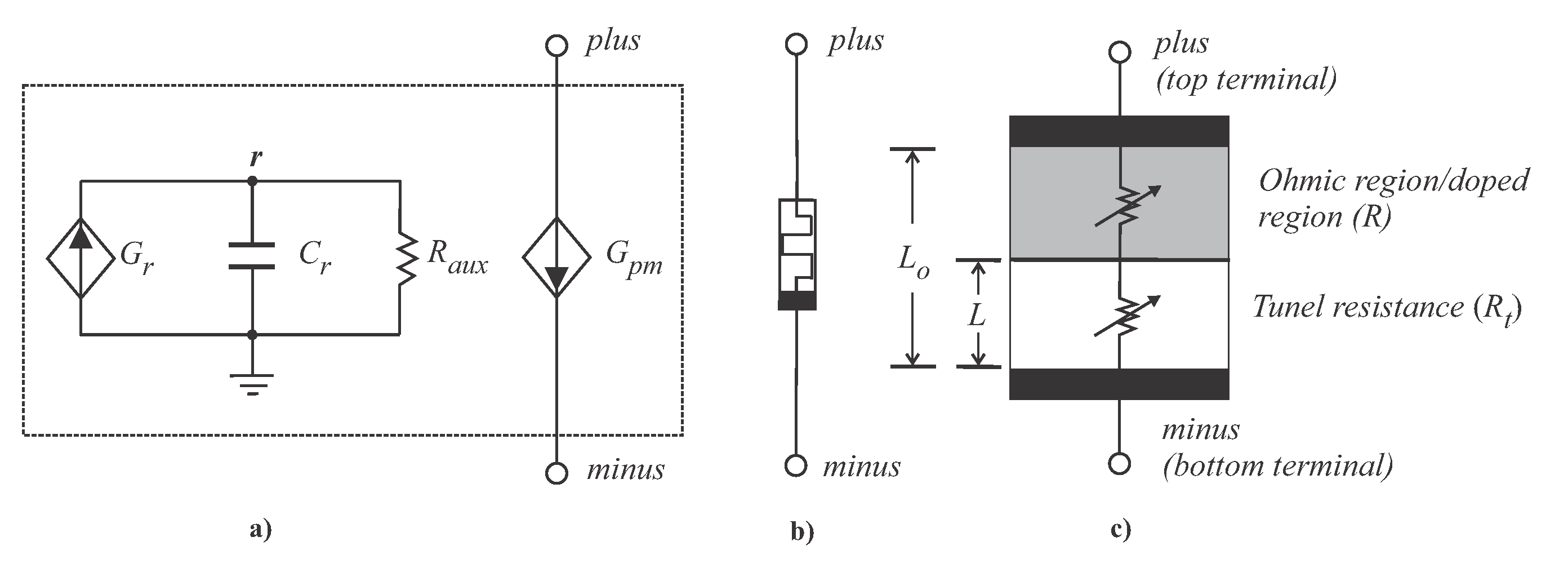
Figure 1. Cross-seccion of a memristor device and macromodel: (a) Macromodel equivalent electrical circuit, (b) Electrical symbol, and (c) Cross-section view.
Preprints 107862 g001
Figure 2. Circuit abstraction to produce STDP learning rule. The left terminal of a memristor device is connected to the output of a pre-synaptic spiking neuron, and its right terminal is connected to the input of a post-synaptic spiking neuron. The former has to feed back its output to its input whenever it generates a spike. Also, the right terminal must be chosen as the top or bottom terminal of the memristor (indicated by the fabricant) to conduce to lower the memristance (increase conductance) if the pre-synaptic neuron fires before the post-synaptic neuron inside a time window as molded by 8.
Preprints 107862 g002
Figure 3. Schematic diagram of the proposed LIF neuron, inspired from in [22]. The main components are the integrator and buffer block. Depending on the ϕ i n t and ϕ f i r e signals is the function this block assumes as the voltage-controlled switches modify the configuration of the op-amp that can act as a buffer or an integrator (where the R l e a k y and C m e m components determine the time constant for the integration). Also, the threshold comparison and firing mechanism block work with the control signals generator and the spiking generator block to obtain the desired output voltage shape of the neuron.
Preprints 107862 g003
Figure 4. In a neural network, a LIF neuron located in the hidden layer receives input in the form of the sum of currents from the previous layer ( I i n ). Each incoming current has an amplitude that is proportional to the product of the memristor conductance ( G i ), times the output voltage ( V o u t i ) of the i-th neuron in the previous layer. The LIF neuron then integrates the incoming current, and if it exceeds a certain internal threshold, it fires and sends its potential ( V o u t ) to all the neurons in the following layer.
Preprints 107862 g004
Figure 5. Time diagram of the control signals for the spike generator block on the LIF neuron.
Preprints 107862 g005
Figure 6. Control signals generator block. Proposed circuitry using commercially available components to produce the neuron control signals ϕ i n t , ϕ f i r e , ϕ 1 , and ϕ 2 . When the membrane voltage V m e m reaches the threshold neuron threshold voltage V t h , the signal V c o m p changes from a low to a high state, triggering a sequence of signals as shown in Figure 5.
Preprints 107862 g006
Figure 7. Spiking generator block: Proposed circuitry, using commercial components to generate the spike voltage shape.
Preprints 107862 g007
Figure 8. Output spikes generated by the LIF neuron in the simulator LTSpice.
Preprints 107862 g008
Figure 9. Block diagram of the methodology used for the characterization of the spiking neuron in simulation.
Preprints 107862 g009
Figure 10. In red is presented the tuning curve of the simulated LIF neuron, in blue is presented the function approximation of recorded data.
Preprints 107862 g010
Figure 11. 3D Render of the PCB design of a LIF neuron.
Preprints 107862 g011
Figure 12. Output spikes generated by the physical implementation of the LIF neuron and monitored in the keysight MSOX6004a oscilloscope.
Preprints 107862 g012
Figure 13. Setup for the test-bench of the spiking neuron, in the upper part is the oscilloscope, in the lower part the dual voltage supplies for the PCB, an additional voltage supply for a separate input signal for the spiking neuron.
Preprints 107862 g013
Figure 14. Block diagram of the proposed methodology for the characterization of the spiking neuron.
Preprints 107862 g014
Figure 15. in Blue the tuning curve from the simulation, in red are the data points for the tuning curve obtained with the physical neuron, and in the dashed black line is the approximation with least squares of the experimental data.
Preprints 107862 g015
Figure 16. The upper graph shows a train of spikes with a voltage that surpasses the positive voltage threshold of the memristor; simulating the LTP of a memristive synapse, lowering the resistance of the device. The middle graph shows the change through time in the memristor, and the lower graph shows the configuration of two neurons in series with a memristor between them to act as a synapse. The lower graph shows the connection between the neurons and the memristor to achieve the potentiation.
Preprints 107862 g016
Figure 17. In the top graph is shown the simulation of multiple cycles of potentiation and depression of a memristive synapse with the STDP process; In the middle graph is represented in green the voltage difference between the memristor terminals and in red and blue the upper and lover voltage thresholds respectively; in the bottom graph is shown the configuration of the neurons, in which the output of two neurons are connected with a memristor.
Preprints 107862 g017
Figure 18. a) typical STDP curve presented in living organisms [33]. b) STDP curve achieved with memristive synapses and the SNN neuron developed.
Preprints 107862 g018
Table 1. Comparison table of the main characteristics for the integration and buffer opamp.
Value presented in [22] LTC6268[23] ADA4860[24]
Rise speed [ V μ s ] 784 400 695
Fall speed [ V μ s ] 500 260 560
DC Gain [dB] 72 - -
Unity gain
at frequency[MHz] 272 350 230
Table 2. Comparison table of the main characteristics for transmission gates.
ADG619[26] ADG733[27] ADG788[28]
On-resistance [ Ω ] 6.5 4.5 4.5
On-resistance
flatness [ Ω ] 0.7 0.5 0.5
Dual supply range [V] ± 5 ± 2.5 ± 2.5
Propagation delay
to on condiciont ( t o n )[ns] 40@3.3V 21@1.5V 21@1.5V
Disclaimer/Publisher’s Note: The statements, opinions and data contained in all publications are solely those of the individual author(s) and contributor(s) and not of MDPI and/or the editor(s). MDPI and/or the editor(s) disclaim responsibility for any injury to people or property resulting from any ideas, methods, instructions or products referred to in the content.
Copyright: This open access article is published under a Creative Commons CC BY 4.0 license, which permit the free download, distribution, and reuse, provided that the author and preprint are cited in any reuse.
Prerpints.org logo

Preprints.org is a free preprint server supported by MDPI in Basel, Switzerland.

Subscribe

© 2024 MDPI (Basel, Switzerland) unless otherwise stated