
Submitted:
03 June 2024
Posted:
04 June 2024
You are already at the latest version
Abstract
Due to advances in power electronics technology and the evolution of automation devices, the number of electrical devices that are sensitive to power quality is rapidly increasing, and for this reason, users are increasing their demand for high quality. To meet power quality demands, many power conversion devices are used, including dynamic voltage restorers (DVRs). DVRs are rec-ognized as devices that can effectively manage problems such as voltage segment, swells, and harmonics. DVR control requires many samples for harmonic compensation, which has the dis-advantage of being complicated to implement due to fast digital signal processing computation and the application of the cyclic discrete Fourier transform. In this paper, a high-precision DVR system configuration is proposed that compensates for harmonics using a periodically equivalent time-interval sampling technique and a novel circular structured memory filter. The proposed circular structured multi-pointer memory filter is an effective filter algorithm for high-precision input voltage measurement because it can remove noise and compensate for the delay of the phase angle of the filter in voltage measurement. A simulation and DVR prototype system was built, and the feasibility and effectiveness of the phase angle multi-filter voltage detection method and the compensation method were verified by experiments.
Keywords:
dynamic voltage restorer
; voltage measuring filter
; phase angle multiple pointer
; circular structural memory filter
; equivalent sampling
1. Introduction
To cope with the rapid increase in power demand, power generation, transmission, and distribution facilities need to be expanded. However, owing to various civil complaints, it is not possible to use long-distance power to construct power generation facilities close to the area of demand. In response to these line stability risks, active research is being conducted into the application of technologies that use power semiconductor devices for power transmission lines [1,2,3]. In power transmission systems, voltage controllers are generally divided into first, second, and third stages [4,5]. The first-stage control was performed by an automatic voltage regulator (AVR) mounted on the generator, which operated very quickly in the range of a few seconds. The second-stage control is performed by flexible AC transmission systems (FACTS), static var compensators (SVC), and synchronous compensator. The secondary controllers usually have an operating constant of several seconds. The third-stage control, voltage control, is performed through a device such as a DVR taking into account the stability or economy in the state of secondary control. Secondary control has been actively researched. The representative technologies are FACTS and SVC [6,7,8,9].
2. Voltage Regulator on a Power Line
The structure of the conventional under load tap changer (ULTC) is shown in Figure 1. As shown in Figure 1, the ULTC consists of a transformer with a tab, a tap-switching device with a motor driving element, a dead band, a time delay, an automatic voltage regulator, and a voltage and current measuring device for line voltage compensation. The ULTC switches the tab of the transformer winding during loading and maintains a constant transformer output voltage during load fluctuations. Furthermore, two types of nonload tab-switching devices (NLTCs) and load tab switching devices (OLTCs), and ULTCs are typically applied to large-capacity transformers [10,11].
To eliminate the arcing voltage caused by the load current when switching the taps of the NLTC, a specific tap of the transformer is selected with a tap selector in the no-load condition, and the changeover switch is then moved to the center. In the ULTC, both taps are connected simultaneously when the taps are switched, and the internal circulating current flows owing to the potential difference. A transition resistor (current-limiting resistor) or a reactor is typically installed to suppress the circulating current [12,13].
Figure 3 shows the tap–switch circuit with two taps using a static switch. In the figure, R1 and R2 are resistors that limit the short-circuit current that occurs during the tap switching. In this topology, the RMS voltage is measured in a half-cycle unit, and when switching is required, the voltage is compensated using S1-S8 [14].
3. Electronic DVR
3.1. DVR Topology Characteristic Analysis
Figure 4 shows the basic principle of the DVR. As a rule, the grid voltage contains the fundamental wave voltage, the DC voltage, and the number of harmonics, as shown in Equation (1).
Therefore, the DVR must not only control the fundamental wave voltage, but also remove the harmonic components of the DC power voltage and grid voltage. For the DVR to operate at the grid voltage indicated in Equation (1), the DVR power converter must generate the voltage shown in Equation (2):
If the DVR power converter generates the same voltage as shown in Equation (2), the output voltage may theoretically generate a constant voltage sinusoidal wave, as shown in Equation (3), as the sum of Equations (1) and (2) in a structure in which the grid voltage and DVR power converter are connected in series, as shown in Figure 4a.
Figure 4b shows the above explanation.
There are various methods to implement a DVR system; a representative method is shown in Figure 5 [15,16].
Figure 5a shows a commonly used transformer with a low boosting ratio to connect it in series with the grid voltage, and the inverter is driven at a high voltage. This method has the advantage that the current rating of the inverter can be lowered by increasing the inverter driving voltage and using a transformer. However, it should be noted that the inverter overvoltage during initial input and light load is a problem when the inverter is not operating. In addition, the inverter output voltage to compensate for the output voltage is influenced by the inverter arm voltage and the internal parameters of the transformer, capacitors, and loads. In particular, there is a limit to harmonic compensation as the phase difference between the inverter output voltage and the inverter arm voltage increases with increasing frequency.
With recent developments in semiconductor devices and power electronics, methods such as the one shown in Figure 5b are becoming more common. This method also has similar characteristics to the previous method in terms of the relationship between the inverter output voltage and the inverter arm voltage to compensate for the output voltage. When the inverter arm terminal voltage is expressed by Equation (2), the inverter output voltage is expressed by Equation (4).
3.2. G : Inverter Arm Voltage Transfer Function
In Equation (4), G is the transfer function of the inverter arm voltage from the inverter output voltage, which is the voltage required to compensate for the output voltage for each frequency. In general, G is negligible because the change in magnitude is very small; however, the phase difference cannot be ignored as the frequency increases [17,18].
Figure 6 shows a vector diagram for each voltage in the topology shown in Figure 5b. Figure 6a shows a vector diagram of the fundamental wave, where the output voltage is represented by the sum of the inverter output voltage and the grid voltage, whose phase is different from the grid voltage through the LCR filter in the inverter arm voltage. The desired voltage control is possible through the feedback control of the output voltage.
Figure 6b is a vector diagram for harmonics. As is evident in the figure, a voltage with a phase difference of 180 ° is generated for the harmonic component of the grid voltage; however, the harmonic component cannot be removed through the LCR filter because of the difference between the power supply voltage and the phase. Even if the inverter output voltage is in phase with the harmonic component of the power supply voltage, there is a risk of control divergence [19].
3.3. Proposed DVR Topology
The topology mentioned in the previous section proposes a new topology, as shown in Figure 7, to solve the drawback of the incomplete compensation of the harmonic components with the inverter’s output voltage phase. The proposed topology is characterized by a filter structure that delays the grid voltage and inverter arm voltage simultaneously in the same phase. This structure has the advantage that the phase delay does not have to be considered.
In this study, the inverter arm voltage was determined based on the command voltage of the compensation inverter as shown in Equation (5):
The grid and inverter arm voltages, which are connected in series, are therefore expressed equivalently, as shown in Equation (6).
The voltage in Equation (6) forms the output voltage of the LCR filter and is expressed by Equation (7). As is evident from this equation, the magnitude of the output voltage changes slightly; however, only the fundamental wave voltage is generated when the harmonic voltage is removed.
Figure 8 shows a vector diagram for each voltage in the topology shown in Figure 7. Figure 8a is a vector diagram for the fundamental wave. As is evident in the figure, the grid voltage and the inverter arm voltage are in the same phase, and the sum of the two voltages is represented as the output voltage with a phase difference from the grid voltage through the LCR filter. Accurate voltage control can be achieved by feedback control of the output voltage.
Figure 8b is a vector diagram for harmonics, and as is evident in the figure, the harmonic component becomes zero by generating a voltage with a phase difference of 180 degrees with respect to the harmonic component of the grid voltage and passing it through the LCR filter. Therefore, this topology has the advantage of being able to remove harmonic components regardless of the value of the LCR filter.
In other words, the existing DVR receives the inverter output voltage, whose phase is changed after passing through the LCR filter from the inverter arm voltage, which it uses as the inverter output voltage for direct output compensation. This has the advantage that the harmonic component is not considered.
3.3. Multi-Pointer Memory Filter with Circular Structure
In general, an analog low-pass filter (LPF) with a cutoff frequency much larger than the power frequency is used to remove noise when measuring the grid voltage. The output of the filter then changes in size and phase compared to the input. Especially for periodic sinusoidal waves with the same amplitude and phase, the actual voltage and filter output voltage error were significantly affected by the phase difference generated at the cut-off frequency of the filter. Therefore, to eliminate the phase difference caused by the analog filter and achieve the same voltage as the actual voltage, a circular structure memory filter is proposed, as shown in Figure 9. Here, N represents the number of samples for one voltage period, as shown in Equation (8), and can be shifted by a specific number of offsets in the circular memory.
Figure 10 shows the operating principle of the circular filter. Figure 10 shows the operating principle of the circular filter. The filter output (Vg_f), as shown in Figure 10a, changes in size and phase compared to the input. Figure 10b shows the AD sampling values for a periodic voltage waveform. Figure 10c shows the phase-shifted waveform when the offset is set to 1 in the periodic waveform, which has the same phase as the grid voltage (Vg) in Figure 10a. Thus, using the proposed circular filter structure, the phase delay of the analog filter has been eliminated.
The output of an analog filter with a high cutoff frequency does not block the low- and mid-order harmonic components and appears in the measured voltage; the white noise component of the AD conversion is also included in the measured voltage. In general, a digital low-pass filter with a lower cutoff frequency than that of an analog filter is used to remove harmonic components and noise. However, digital filters cannot be used as circular filters. In particular, a considerable amount of time is required to filter all frequency components using a single-structure filtering method. Therefore, in this paper, a multi-pointer memory filter with circular structure is proposed, as shown in Figure 11. The proposed circular-structured multi-pointer filter requires N digital low-pass filters. In this paper, the first-order low-pass filter is defined by Equation (9):
The proposed multiple-pointer filter requires N filters. However, the sampling frequency of the filter is 60 Hz, which corresponds to the period of the grid voltage frequency. Therefore, as one filter calculation is required within one cycle of power input, the calculation time for N low-pass filters is the same as that for a low-pass filter with the sampling frequency of the program. In other words, the multiple-pointer filter structure has a large number of filters, but there is no significant limit to the calculation time.
Figure 12 shows the working principle of a circular multi-pointer filter. In the figure, the red line represents the output of the first filter out of N filters. The figure shows the output of the multi-pointer filter V1f (k) for the discrete input V1 (k) of the filter, and it is evident that the N sampling rates have the same value. It is also evident that the purple color has the same characteristics as the K-th filter output. The unique characteristic of this multi-pointer filter is that each filter takes an input at the same phase angle as the grid voltage, so that the input is recognized as a direct current input rather than an alternating current input, which has the great advantage of forming a low-pass filter without phase delay in its own filter.
4. Simulations and Experiments
4.1. Simulation Results
Figure 13 shows the DVR simulation circuit diagram of the proposed scheme. The simulation circuit consisted of a visual C, a dll unit for the interface, a single-phase full-bridge inverter unit, a grid voltage, and a power filter. To implement the actual grid voltage used in the industrial field, the effective value of the grid voltage fundamental wave was set to 200 V. In addition, the peak values of the three-harmonic, five-harmonic, and seven-harmonic voltages were set to 7 V, 5 V, and 7 V respectively.
Figure 14 shows the simulation results for a multi-pointer filter with a circular structure. The first waveform shows the output of the all-pass filter output and the phase angle with a 90-degree phase to estimate the phase angle of the grid voltage. It is evident that the estimation characteristics of the phase angle (theta) of the grid voltage in the first waveform in Figure 14 are good. The second waveform shows the characteristics of the multi-pointer filter and reaches a steady state within the fifth cycle of the grid voltage ; however, there is a slight phase difference between the two voltages. The third waveform was the waveform with a circular memory filter. In the first 1 cycle of the power supply, the output appears to be zero as it does not reach one cycle of the circular filter. From the 2nd cycle, an output with a low-pass characteristic is formed and a phase shift is performed, leading to a steady state. The figure also shows that the grid voltage and the output of the multi-pointer filter with circular structure are perfectly consistent. Therefore, the filter algorithm proposed in this paper can measure periodic waveforms without phase delay. It is anticipated to exhibit exceptional attributes when used as a feed-forward controller in an AC power supply.
Figure 15 shows the simulation results for analyzing the filter characteristics near the voltage zero point. The cutoff frequency of the grid voltage and the analog filter were set to 900 Hz, and at this point, with a grid voltage of 60 Hz, the gain was 0.998, and the phase delay was approximately 3.8 °. With a phase lag of 3.8 °, the input–output difference was approximately 30 V at 220 V. It can also be seen that the phase-shifted waveform to compensate for the phase difference between the sampled filter voltage output (Vg_f) and the actual grid voltage matches the grid voltage.
Figure 16 shows the simulation results for the DVR voltage compensation. The voltage compensator was controlled after 0.1s considering the time constant of the multi-pointer filter with a circular structure. As a result, the output voltage is estimated from 200 V to the command voltage of 220 V within 4 ms.
Figure 17 shows the waveform of the simulation results of the voltage compensation of the steady DVR. Looking at the first waveform, the grid voltage and the output voltage of the multi-pointer filter with a circular structure are identical, and the inverter output voltage of the second waveform forms a waveform for fundamental wave voltage compensation and elimination of the high-frequency voltage. It is evident that the output voltage, which is the sum of the grid voltage and the inverter voltage, is a 220 V sine wave.
4.2. Experimental Result
Figure 18 shows the experimental waveform of the circular multi-pointer filter. Figure 18a shows the grid voltage, the circular structure multi-pointer filter output, and the analog filter output waveform. It can be seen that setting the cutoff frequency of the circular structure multi-pointer filter to 0.6 Hz to safely remove the noise from the actual voltage results in good characteristics. Figure 18b shows the steady-state waveform of Figure 18a, which is distorted because the grid voltage contains a low-order harmonic component, and also shows that the output of the circular-structure multi-pointer filter almost matches the grid voltage. In Figure 18c, the waveform for the phase stream matches the grid voltage to compensate for the phase difference between the grid voltage (Vg_f) and the actual grid voltage (Vg) sampled in the steady-state waveform shown in Figure 18b [20].
Figure 19 shows the experimental results when the grid voltage changes from no load to a 1.0 kW load in the state of 200 V as in the simulation to analyze the excellence of the characteristics of the proposed system. Figure 19a shows a case controlled by the conventional method, in which a harmonic component appears in the output voltage owing to the harmonic of the grid voltage. As shown in Figure 19b, although there is a harmonic in the grid voltage, in the proposed method, the output voltage becomes sinusoidal with an effective value of 220 V. The technique also exhibits favorable transient characteristics, with minimal voltage sag in the output during power input.
Figure 20 shows the experimental result when the load of the DVR changes from 1.0 kW to 2.0 kW. The test results show that the load fluctuation responds immediately and maintains a constant voltage without a sag at the output voltage.
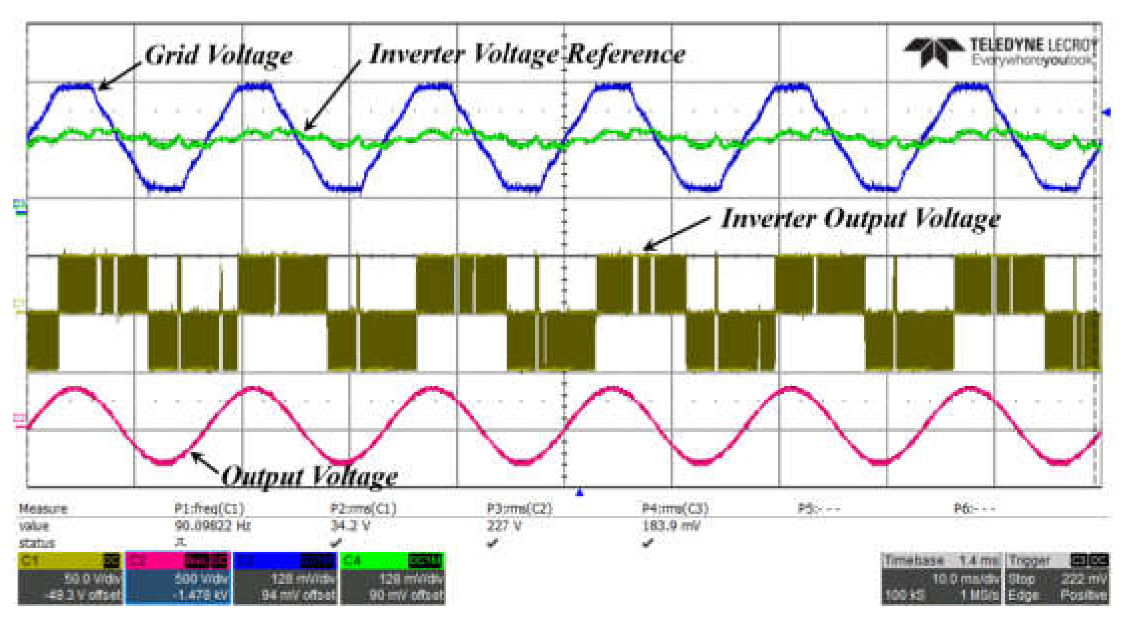
Figure 21 shows the waveform used to analyze the voltage compensation characteristics of the DVR. As shown in the figure, the command voltage waveform of the inverter generates a waveform that removes the voltage and harmonic components to control the magnitude of the fundamental wave voltage from the grid voltage (Vg), which contains the harmonics. A single-phase full-bridge inverter forms a PWM waveform to generate a command voltage. Therefore, when the sum of the grid voltage and PMW voltage passes through the LC filter, a sinusoidal output voltage can be formed.
5. Conclusion
In this paper, a simple topology is proposed that can not only maintain a constant output voltage but also effectively remove the harmonic component of the grid voltage to improve the power quality. The proposed DVR topology connects the grid voltage and inverter output voltage directly and uses the LCR low-pass filter for the sum of the two voltages to remove the harmonic component of the inverter output voltage. In this case, it has the great advantage of not having to take the phase delay of the compensator into account. In addition, a circular structure multi-pointer filtering algorithm has been proposed to remove noise components when detecting the grid voltage, excluding low-frequency filters and harmonic components. The proposed circular structure filter has the advantage of not only being able to arbitrarily perform phase potential, but also having a phase all-pass filter structure without phase delay thanks to its multi-filter structure, regardless of the cutoff frequency of the low-pass filter.
By performing Psim simulations and experiments to verify the validity of the topography and filter structure proposed above, an excellent conclusion was obtained.
DVRs are also used to improve the instantaneous voltage rise (swell) and voltage unbalance as they not only provide reactive power but also have the ability to absorb and are used to reduce harmonics by preventing waveform distortion, comparable to active filters.
Future research plan is the application of DVRs for power compensation in the microgrid field using the equivalent sampling technique proposed in this paper.
Funding
This research was supported by "Regional Innovation Strategy (RIS)" through the National Research Foundation of Korea (NRF) funded by the Ministry of Education (MOE) (2021RIS-002).
Acknowledgments
This study was supported by research fund from Honam University, 2021.
Conflicts of Interest
The author declares no conflict of interest.
References
- M. Rabinowitz, “Power systems of the future.” J. in IEEE Power Engineering Review, vol. 20, no. 1, pp. 5-16, Jan. 2000.
- N. K. Roy and H. R. Pota, "Current Status and Issues of Concern for the Integration of Distributed Generation Into Electricity Networks," in IEEE Systems Journal, vol. 9, no. 3, pp. 933-944, Sept. 2015. [CrossRef]
- E. W. Gunther, “Interharmonics in power systems.” C. 2001 Power Engineering Society Summer Meeting. Conference Proceedings (Cat. No.01CH37262), 2001, pp. 813-817.
- Grzegorz Benysek, Marian Pasko (2012). Power Theories for Improved Power Quality. Springer-Verlag, London.
- T. Tewari, A. T. Tewari, A. Mohapatra and S. Anand, "Coordinated Control of OLTC and Energy Storage for Voltage Regulation in Distribution Network With High PV Penetration," in IEEE Transactions on Sustainable Energy, vol. 12, no. 1, pp. 262-272, Jan. 2021. [CrossRef]
- N.Mahmud and, A. N.Mahmud and, A.Zahedi, “Review of control strategies for voltage regulation of the smart distribution network with high penetration of renewable distributed generation,” Renew. Sustain. Energy Rev., vol. 64, pp. 582-595, Oct. 2016.
- T. Aziz and N. Ketjoy, Enhancing PV penetration in LV networks using reactive power control and on load tap changer with existing transformers, IEEE Access, vol. 6, pp. 26832691, 2018.
- C. R. Sarimuthu, V. K. C. R. Sarimuthu, V. K. Ramachandaramurthy, K. R. Agileswari, and H. Mokhlis, “A review on voltage control methods using on-load tap changer transformers for networks with renewable energy sources,” Renew. Sustain. Energy Rev., vol. 62, pp. 11541161, Sep. 2016.
- H. Xu, A. D. Domínguez-García and P. W. Sauer, "Optimal Tap Setting of Voltage Regulation Transformers Using Batch Reinforcement Learning," in IEEE Transactions on Power Systems, vol. 35, no. 3, pp. 1990-2001, May 2020. [CrossRef]
- Moghassemi, A.; Padmanaban, S. Dynamic Voltage Restorer (DVR): A Comprehensive Review of Topologies, Power Converters, Control Methods, and Modified Configurations. Energies 2020, 13, 4152. [Google Scholar] [CrossRef]
- G. Ram, V. Prasanth, P. Bauer and E. -M. Bärthlei“, "Comparative analysis of on-load tap changing (OLTC) transformer topologi”s," 2014<sup> 1</sup>6th International Power Electronics and Motion Control Conference and Exposition, Antalya, Turkey, 2014, pp. 918-923. [CrossRef]
- A. Ismail, H. Alsuwaidi and A. Elnady, "Automatic Voltage Stabilization Using IGBT Based on Load Tap Changer With Fault Consideration," in IEEE Access, vol. 9, pp. 72769-72780, 2021, doi: 10.1109/ACCESS.2021.3079507.
- G. R. Chandra Mouli, P. Bauer, T. Wijekoon, A. Panosyan and E. -M. Bärthlein, "Design of a Power-Electronic-Assisted OLTC for Grid Voltage Regulation," in IEEE Transactions on Power Delivery, vol. 30, no. 3, pp. 1086-1095, June 2015. [CrossRef]
- R. N. D. C. Lima and J. R. Macedo, "A Novel Switching Methodology for Low Voltage Static Regulators," in IEEE Access, vol. 10, pp. 20745-20763, 2022. [CrossRef]
- Ghosh and G. Ledwich, “Compensation of distribution system voltage using DVR,” J. in IEEE Transactions on Power Delivery, vol. 17, no. 4, pp. 1030-1036, Oct. 2002.
- C. Udayakiran and S. H. Vali, “Design of Battery Energy Storage System (BESS) Support Dynamic Voltage Restorer (DVR) to Reduce the Rating of Voltage Source Converter (VSC) Applied to IEEE 11, 33 & 69 Bus Systems,” 2017 IEEE 7th International Advance Computing Conference (IACC), 2017, pp. 477-481.
- E. K. K. Sng, S. S. Choi and D. M. Vilathgamuwa, “Analysis of series compensation and DC-link voltage controls of a transformerless self-charging dynamic voltage restorer,” J. in IEEE Transactions on Power Delivery, vol. 19, no. 3, pp. 1511-1518, July 2004.
- E. K. K. Sng, S. S. Choi and D. M. Vilathgamuwa, “Analysis of series compensation and DC-link voltage controls of a transformerless self-charging dynamic voltage restorer,” J. in IEEE Transactions on Power Delivery, vol. 19, no. 3, pp. 1511-1518, July 2004.
- Ghosh and G. Ledwich, “Structures and control of a dynamic voltage regulator (DVR),” J. 2001 IEEE Power Engineering Society Winter Meeting. Conference Proceedings (Cat. No.01CH37194), 2001, pp. 1027-1032.
- A.H. Soomro, A.S. Larik, M.A. Mahar, A.A. Sahito, A.M. Soomro, G.S. Kaloi “Dynamic voltage restorer—a comprehensive review” Energy Rep., 7 (2021), pp. 6786-6805. [CrossRef]
Figure 1.
The structure of a typical ULTC. (a) Auto transformer type; (b) Serial transformer type.
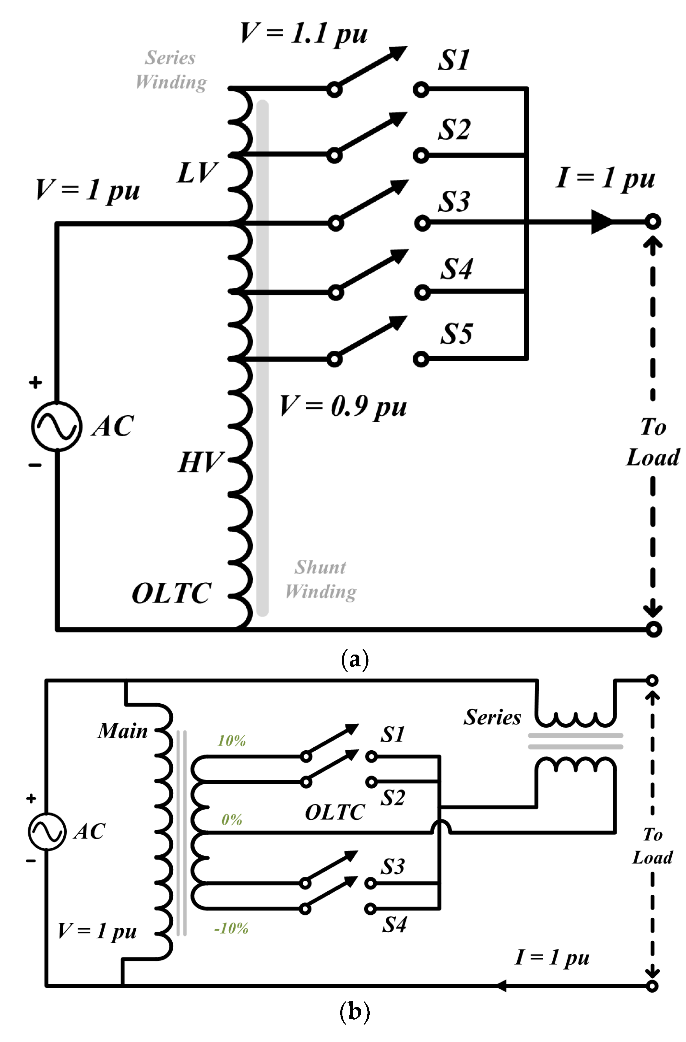
Figure 2.
ULTC tap change operation principle.
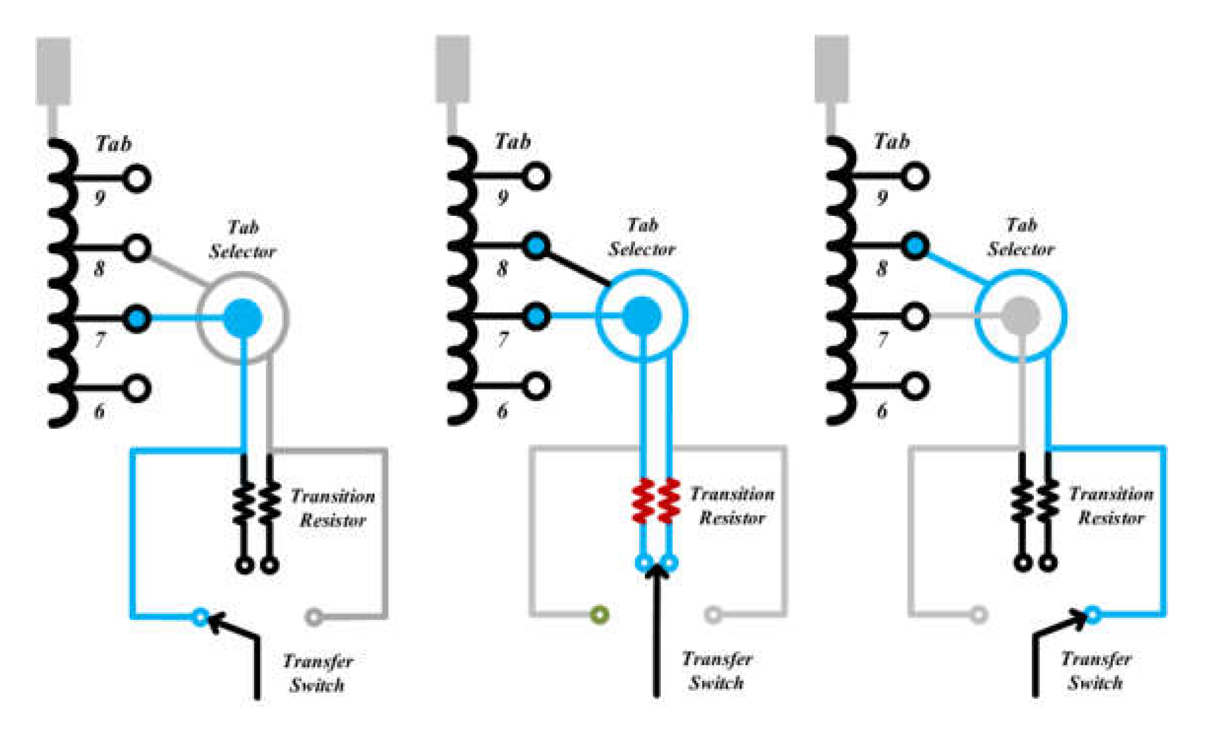
Figure 3.
Tap changer with static switches.
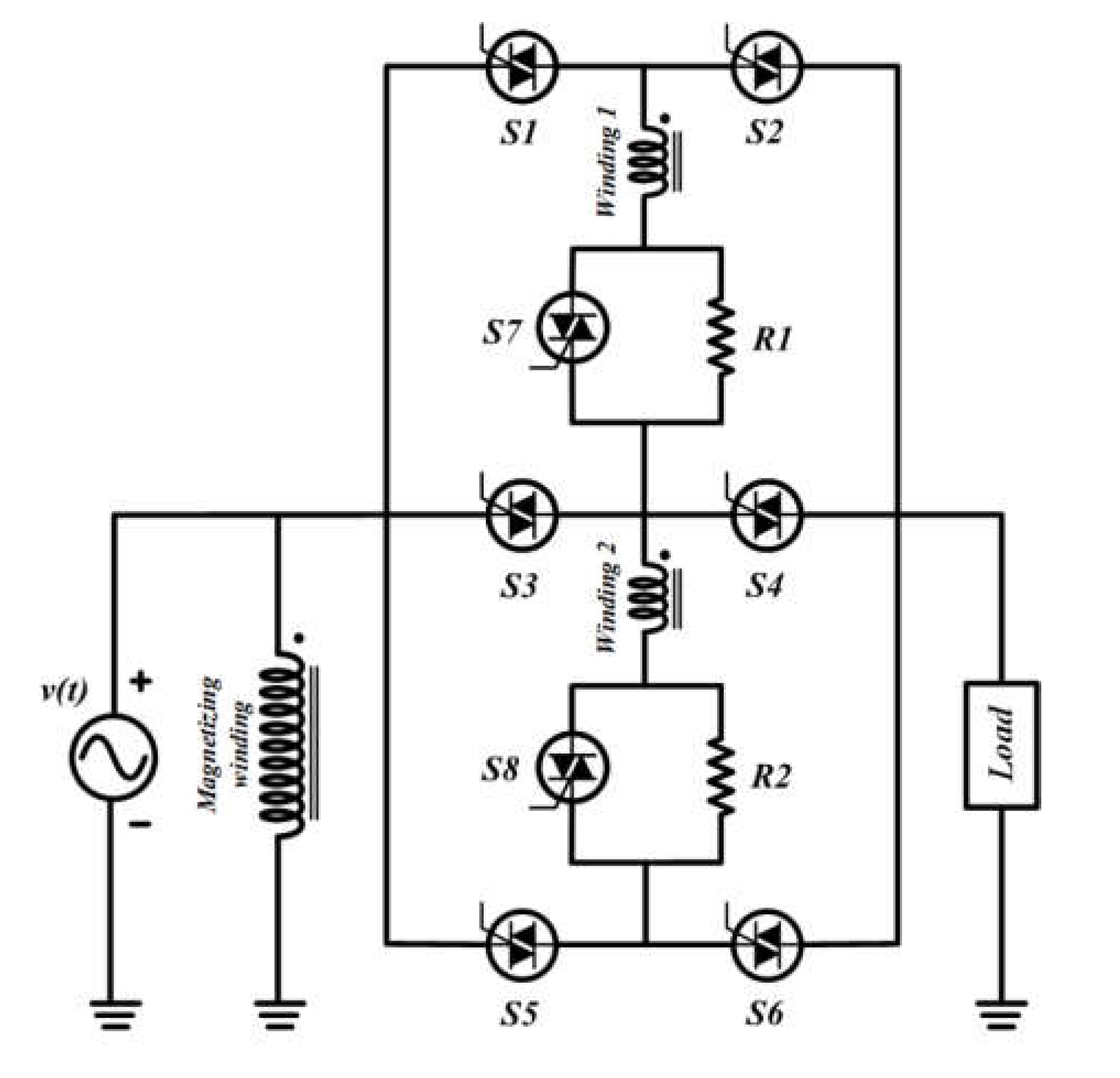
Figure 4.
Basic principles of the DVR.
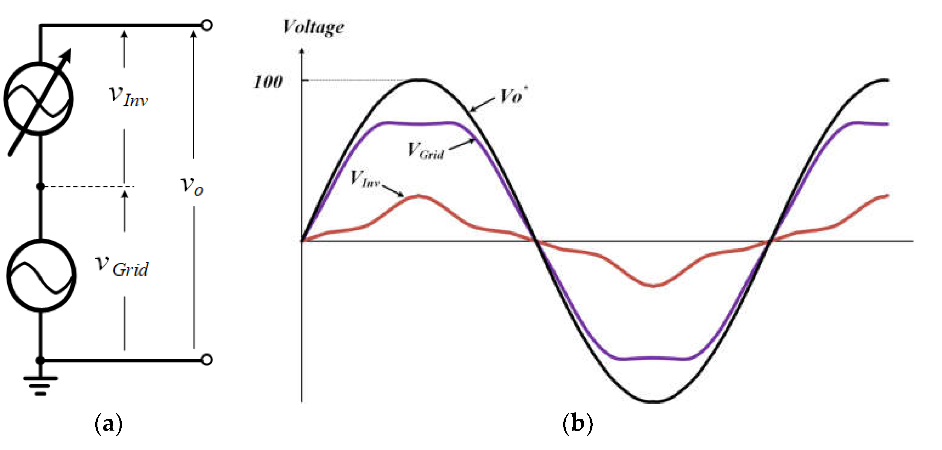
Figure 5.
Typical DVR system configuration.
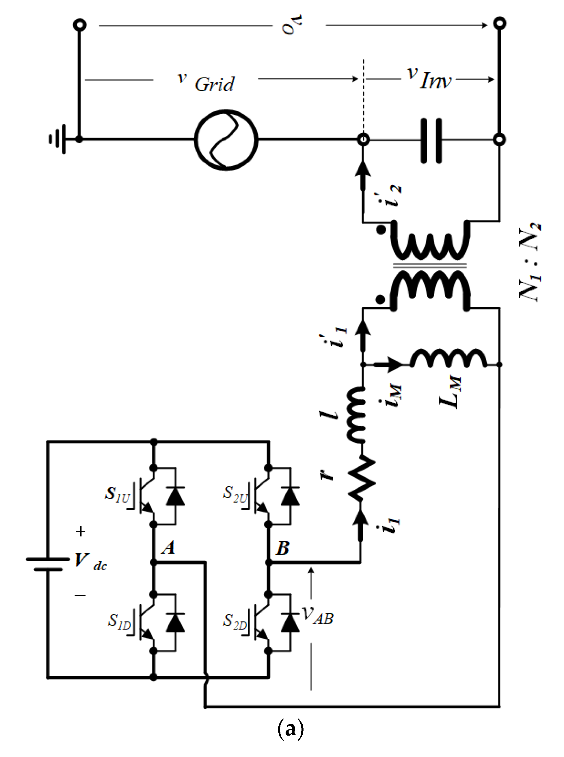
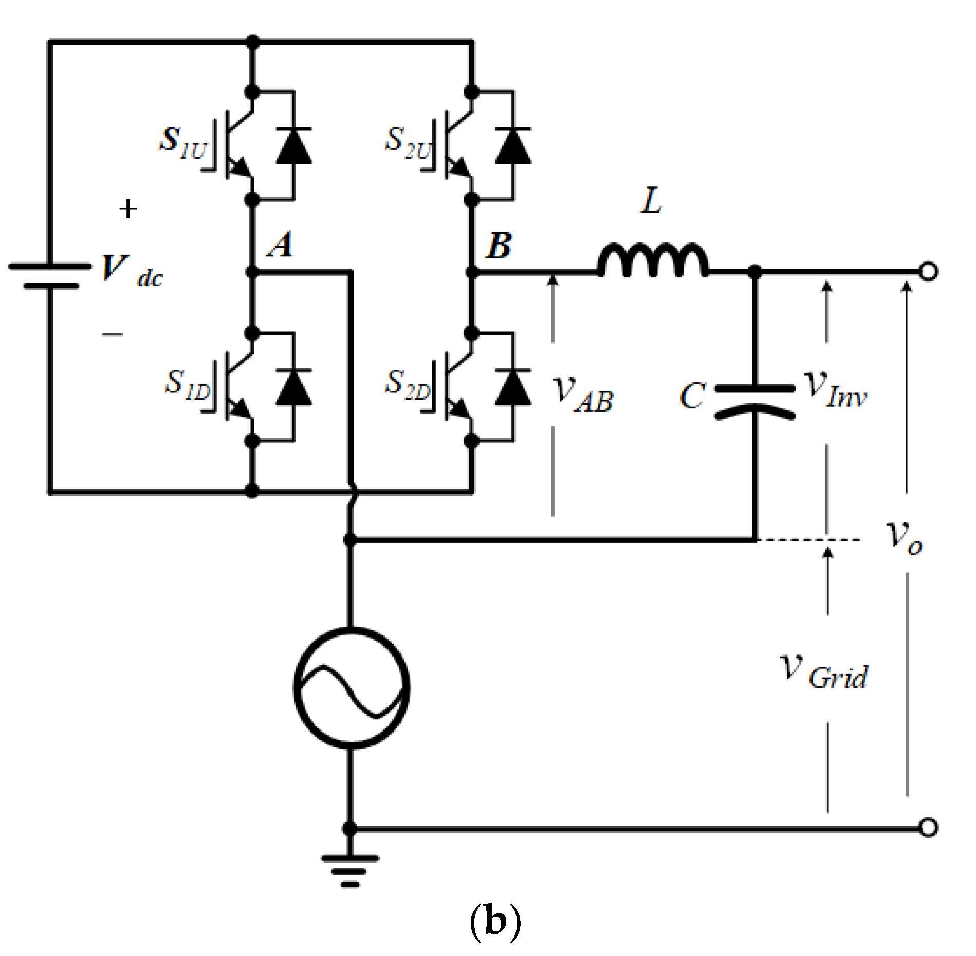
Figure 6.
Compensation characteristics as a function of DVR frequency; (a) Fundamental wave vector; (b) Harmonic vector.
Figure 6.
Compensation characteristics as a function of DVR frequency; (a) Fundamental wave vector; (b) Harmonic vector.
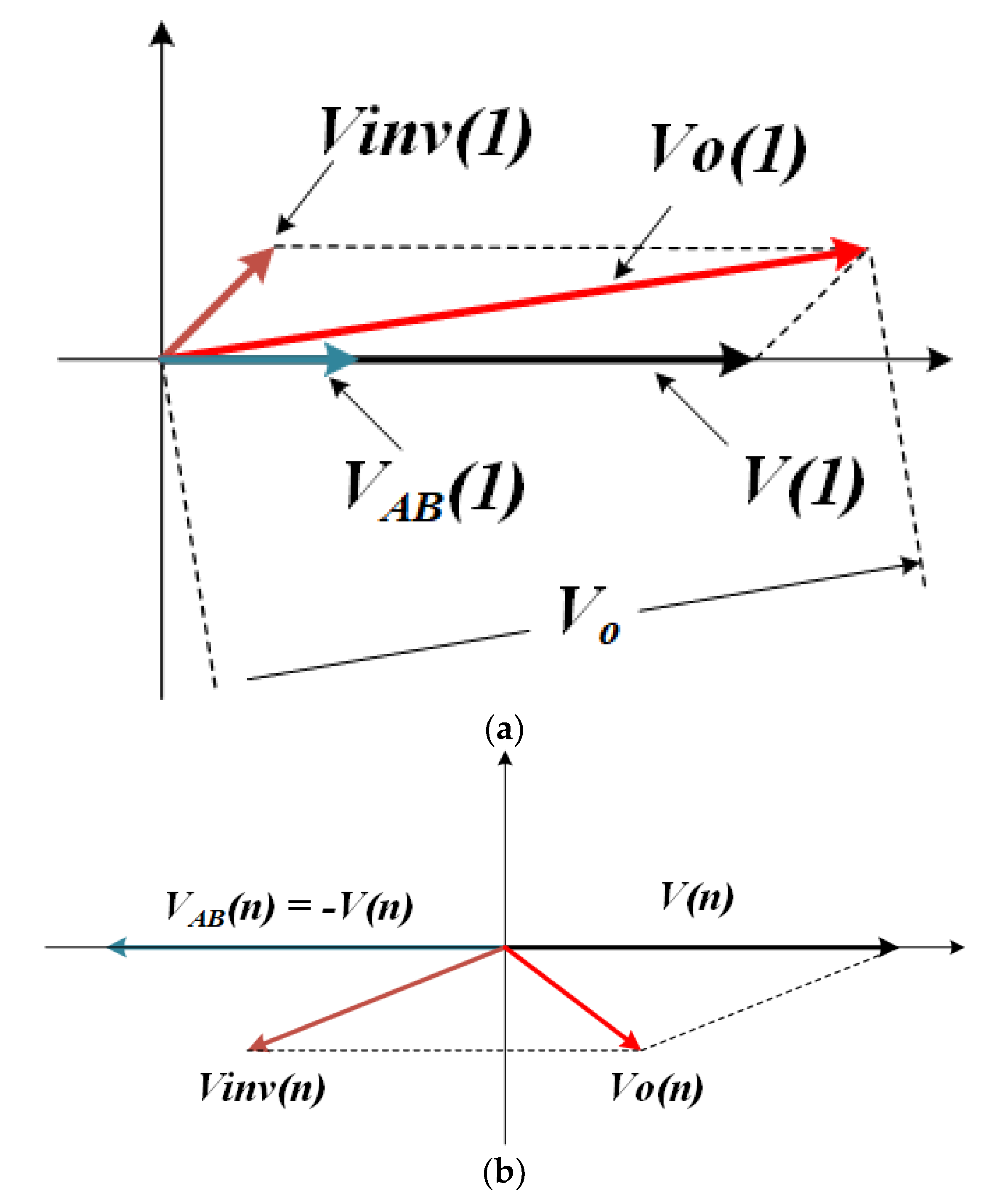
Figure 7.
Proposed DVR system configuration.
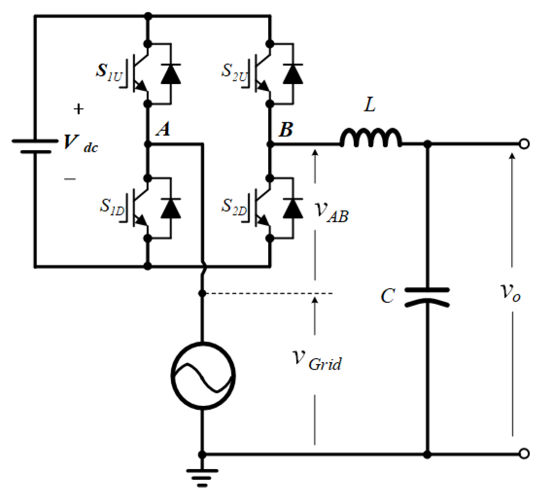
Figure 8.
Compensation characteristics as a function of the frequency of the proposed DVR. (a) Fundamental wave vector; (b) Harmonic vector.
Figure 8.
Compensation characteristics as a function of the frequency of the proposed DVR. (a) Fundamental wave vector; (b) Harmonic vector.
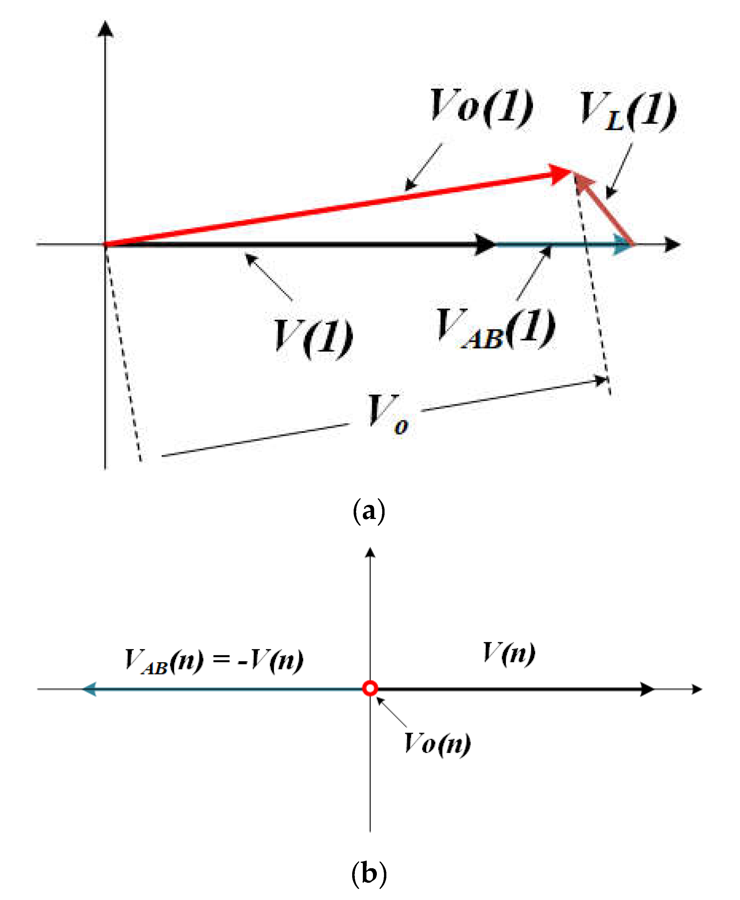
Figure 9.
Circular structure filter.
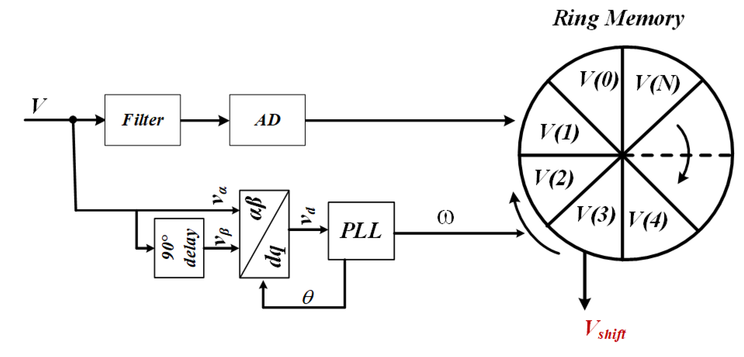
Figure 10.
Operating principle of the circular structure filter. (a) Characteristics of an analog voltage filter; (b) Voltage AD sampling; (c) Phase shift voltage.
Figure 10.
Operating principle of the circular structure filter. (a) Characteristics of an analog voltage filter; (b) Voltage AD sampling; (c) Phase shift voltage.
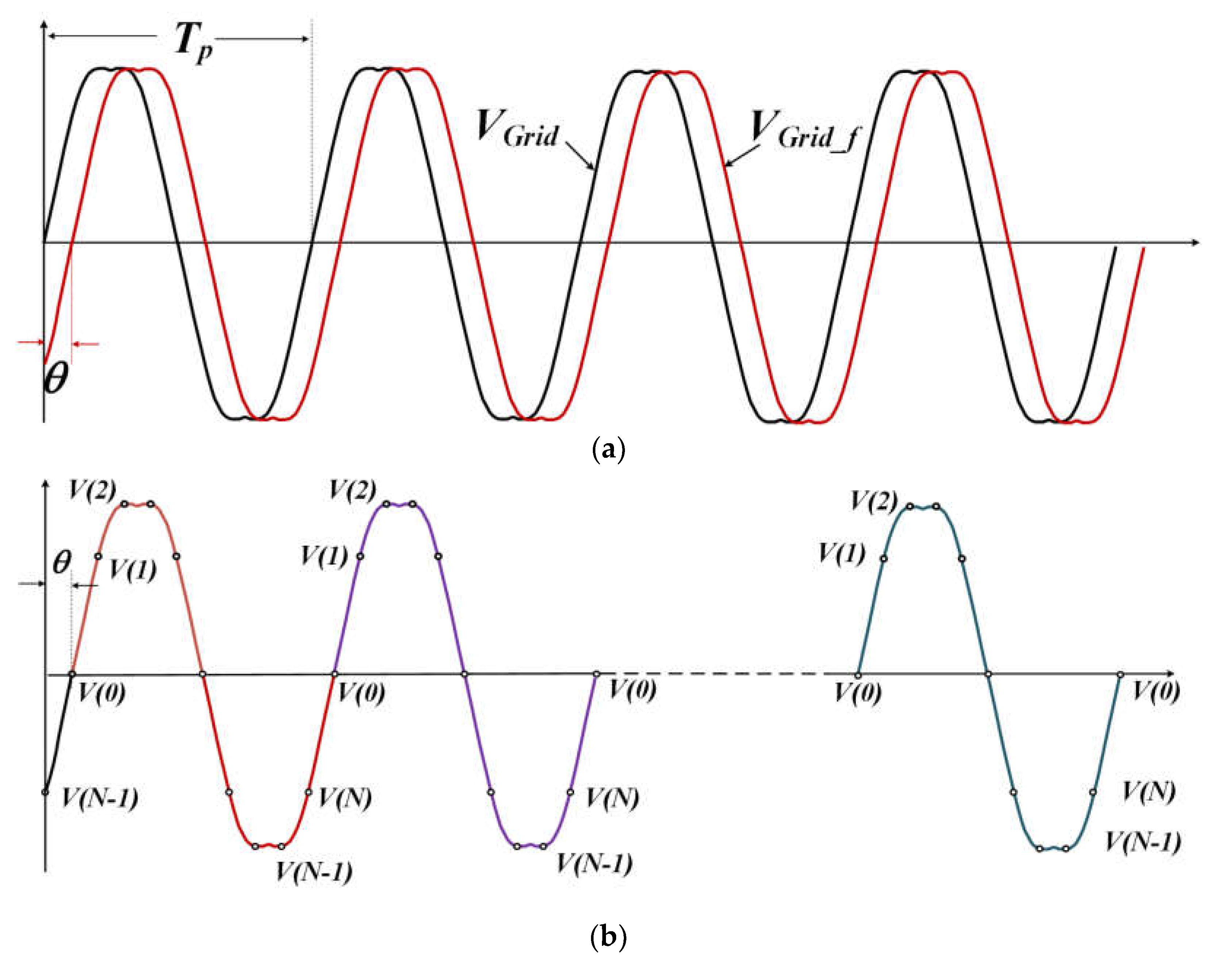
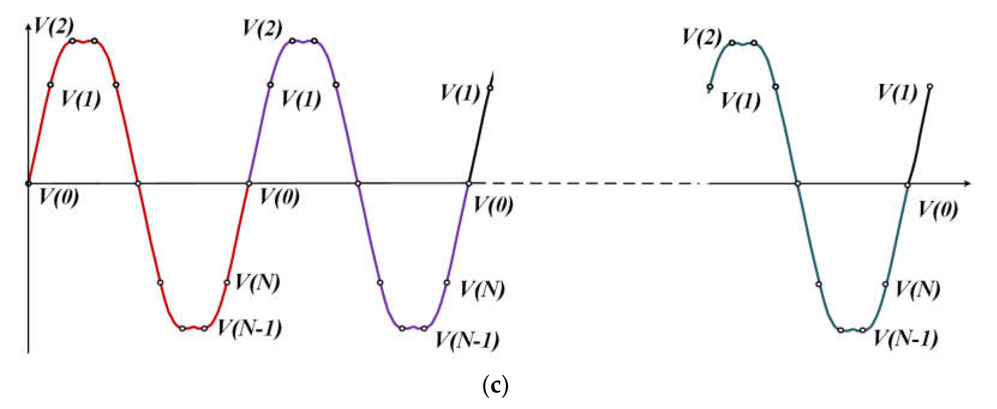
Figure 11.
Multi-pointer memory filter with circular structure.

Figure 12.
Operating principle of the multi-pointer memory filter with circular structure.
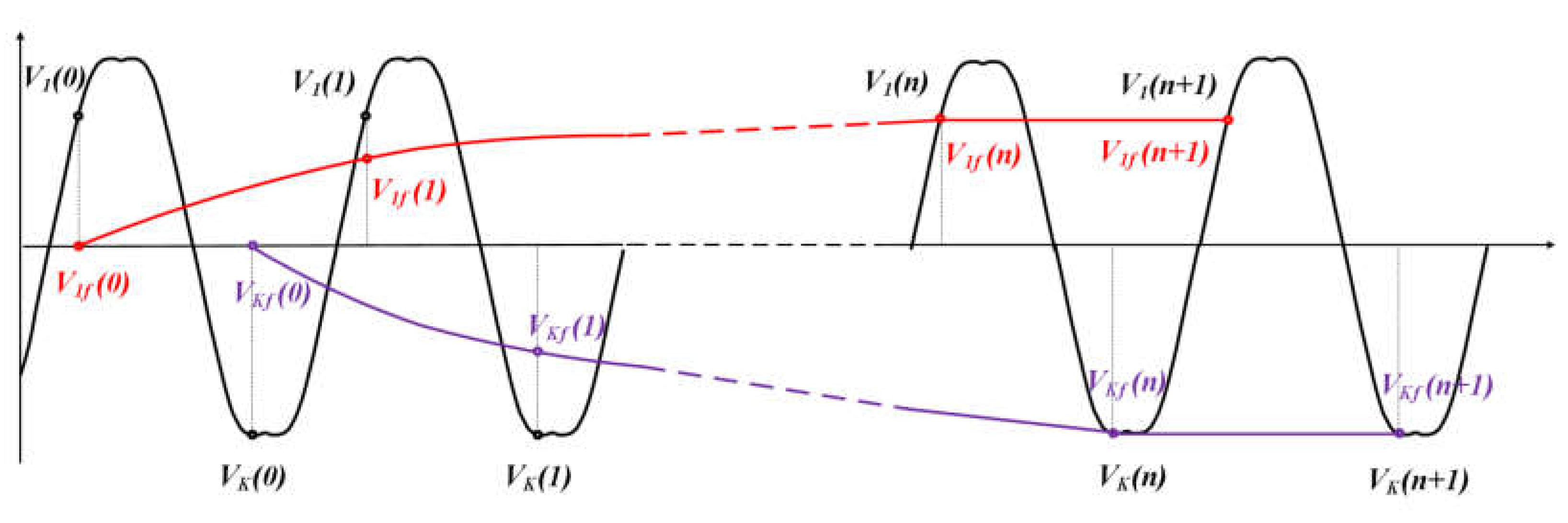
Figure 13.
Circuit diagram for the configuration of the DVR system.
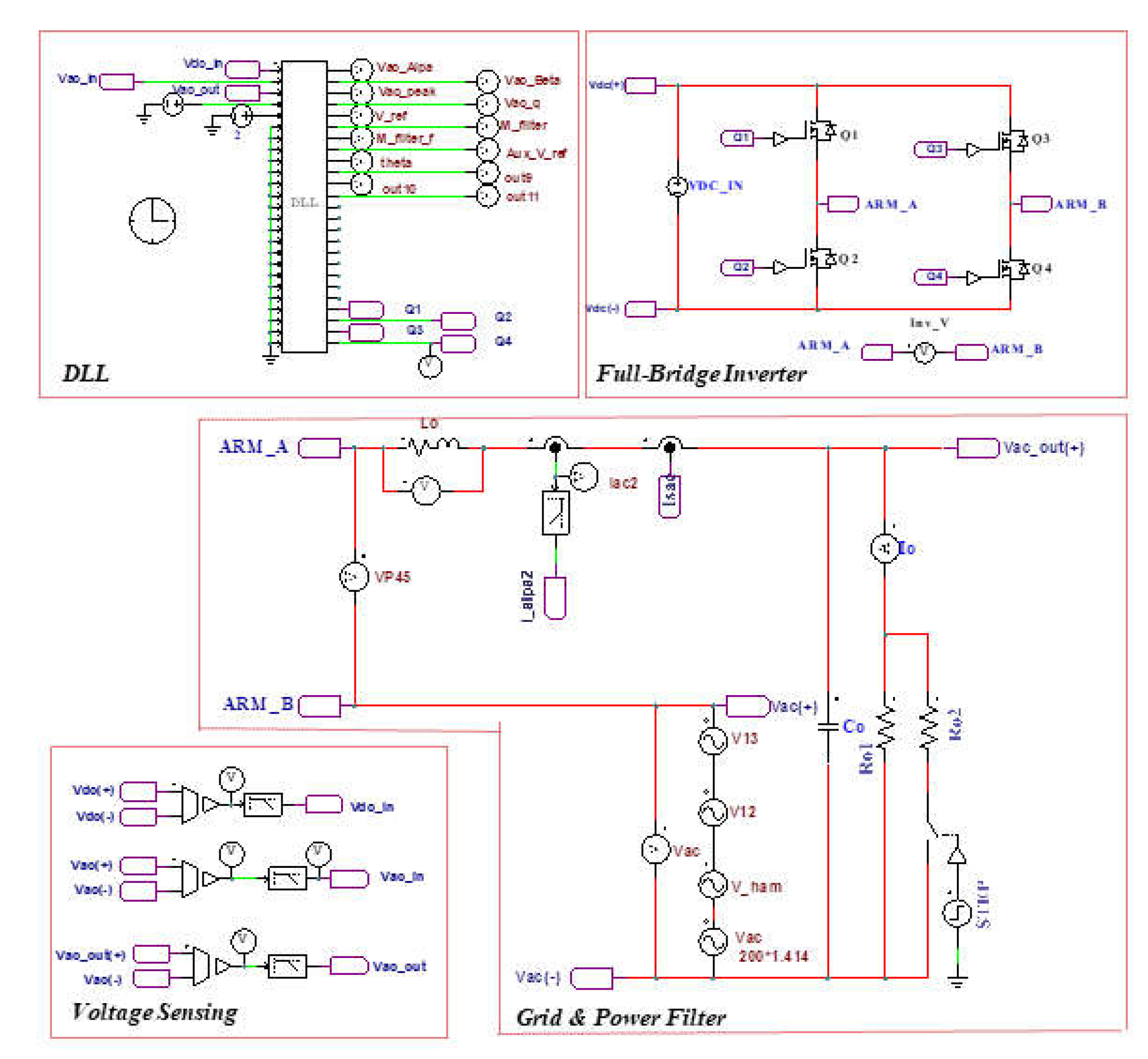
Figure 14.
Simulation results of the multi-pointer memory filter with circular structure.
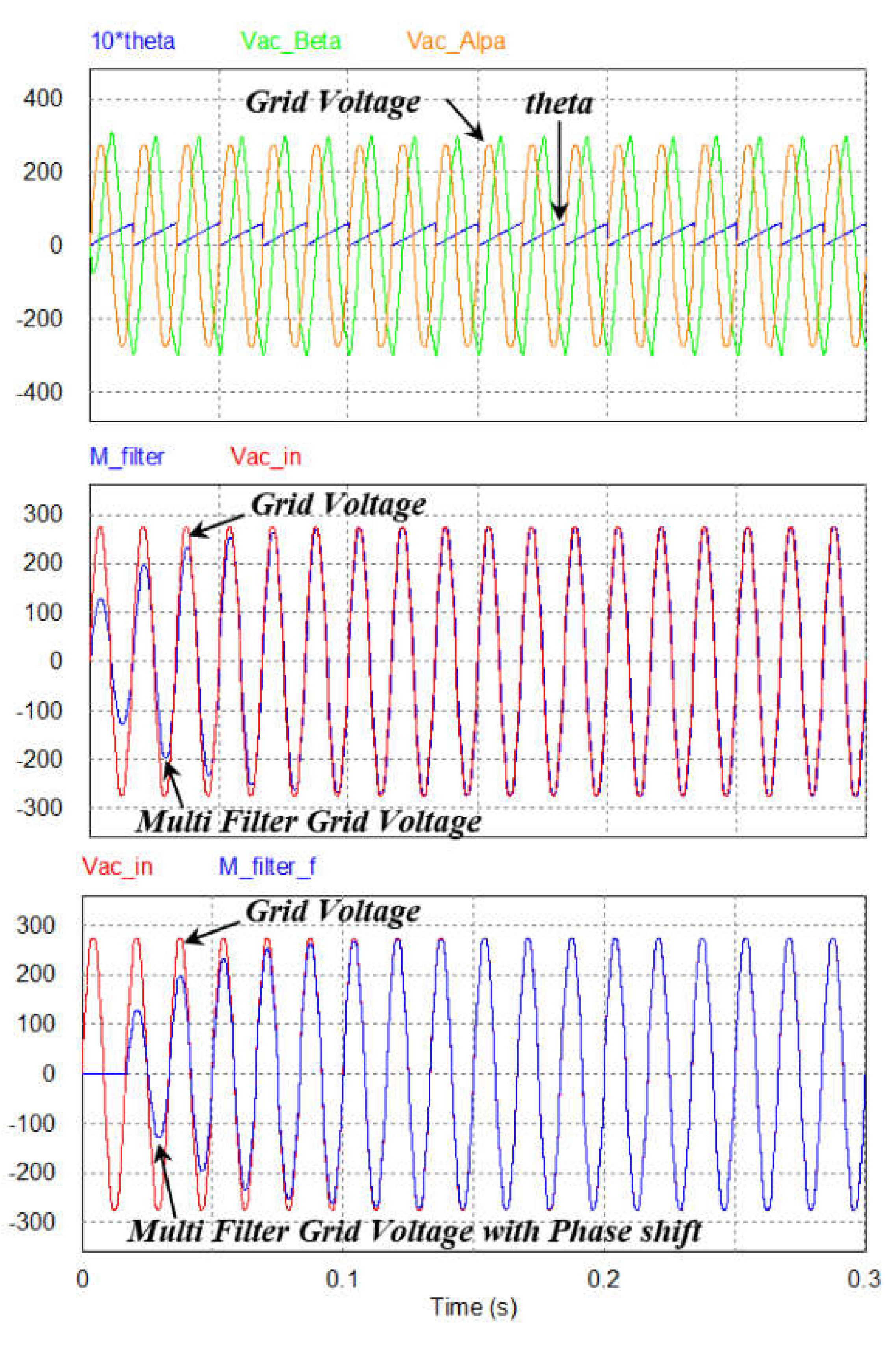
Figure 15.
Simulation results of the filter characteristic analysis near the voltage zero point.
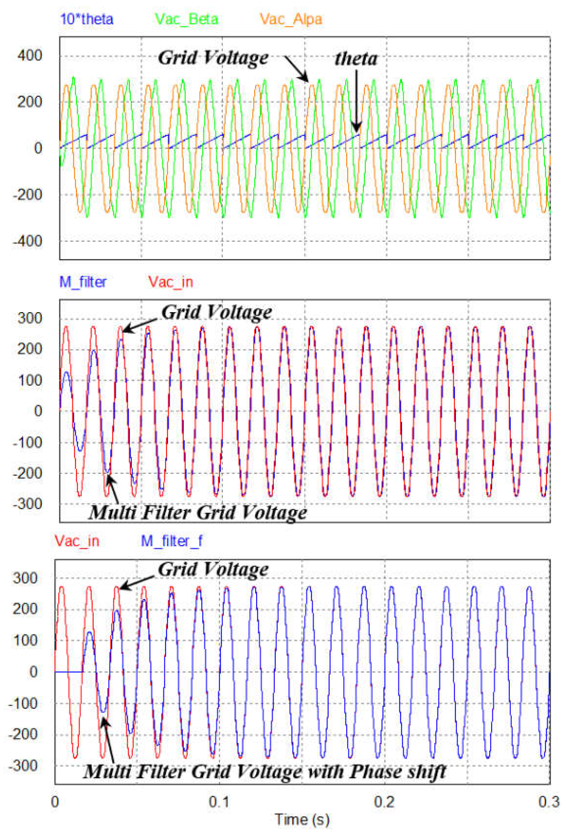
Figure 16.
Simulation result of DVR voltage compensation.
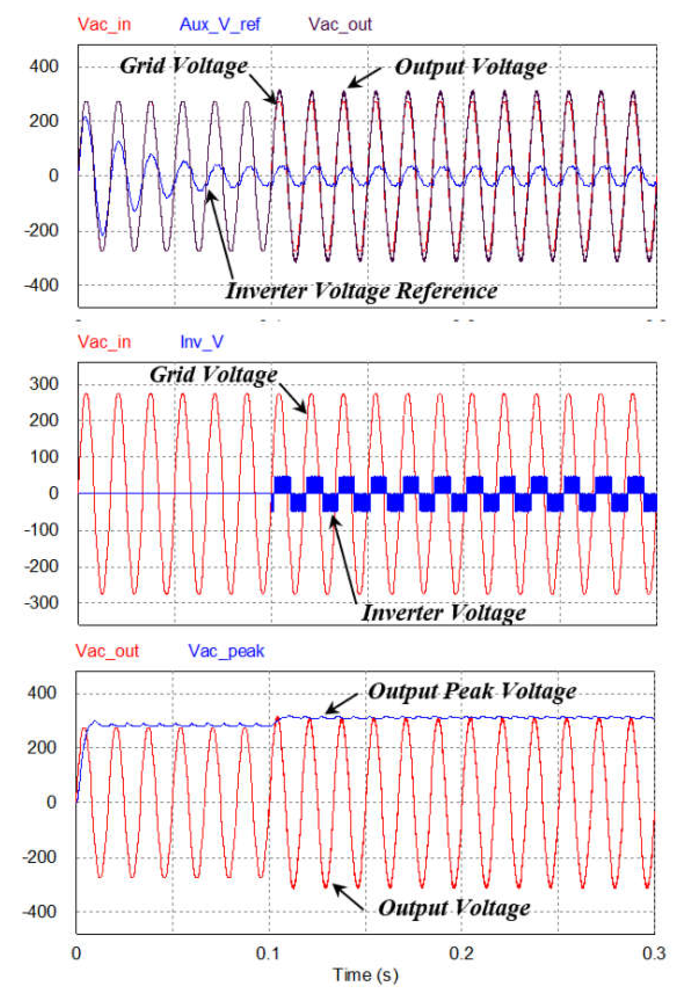
Figure 17.
Voltage compensation simulation results of the steady-state DVR.
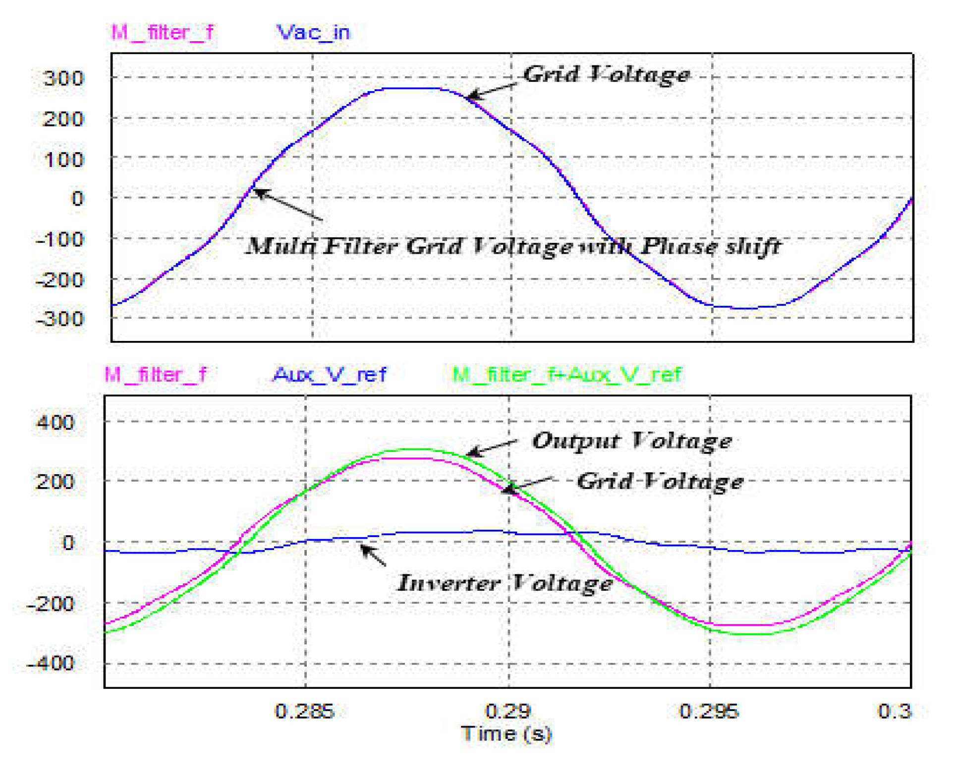
Figure 18.
Filter characteristic analysis.
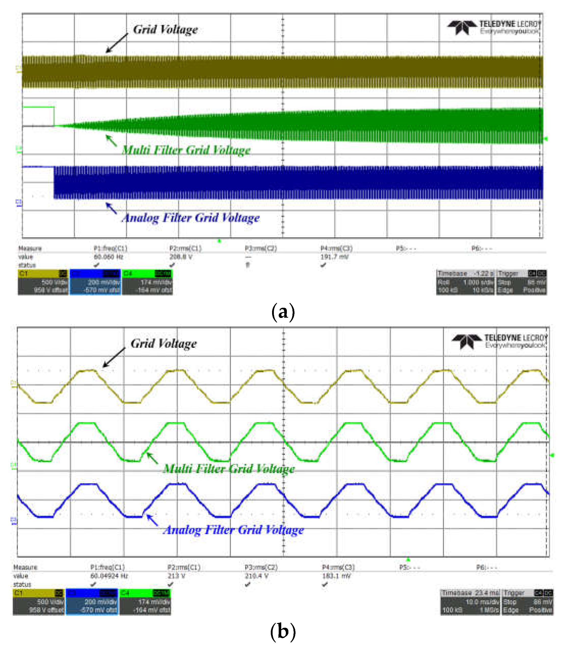
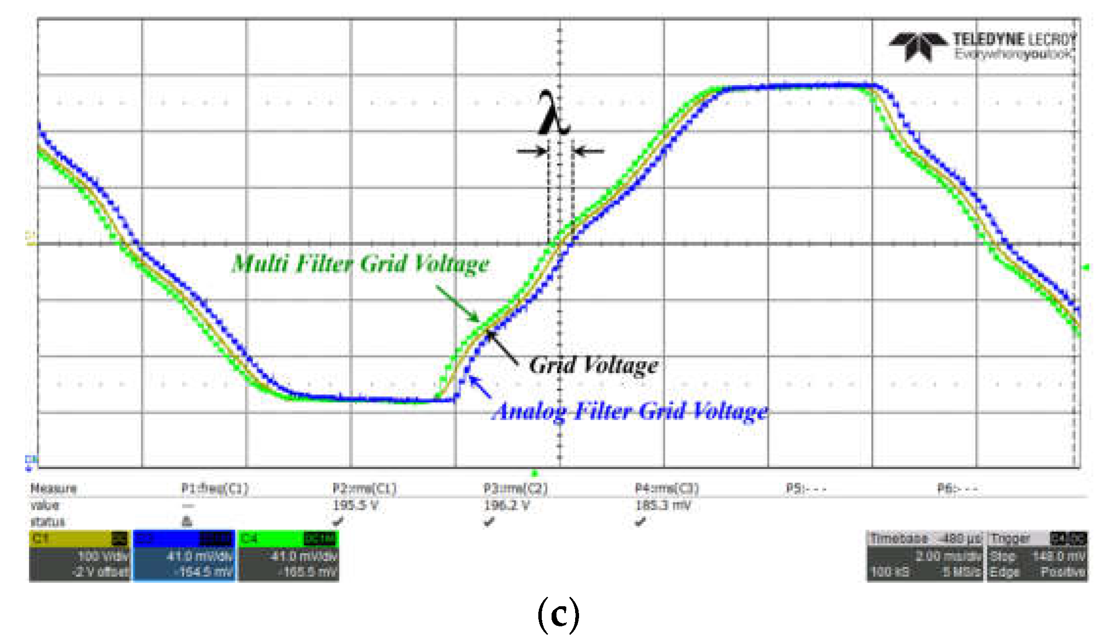
Figure 19.
Results of the DVR voltage compensation experiment.
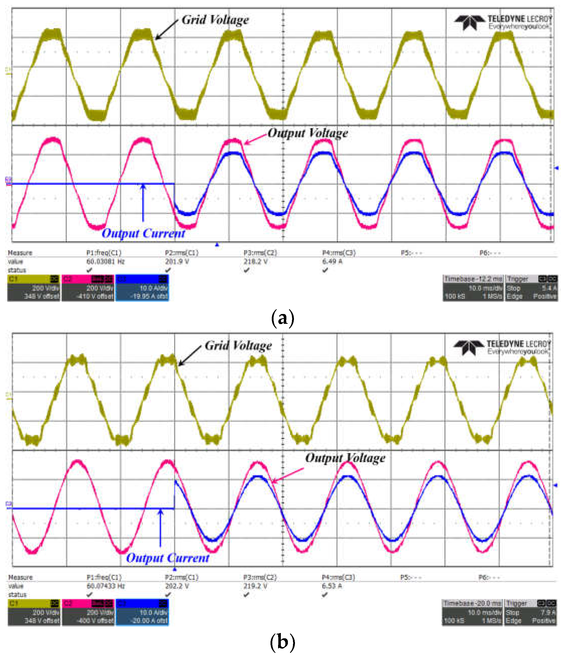
Figure 20.
Results of the DVR load fluctuation experiment.
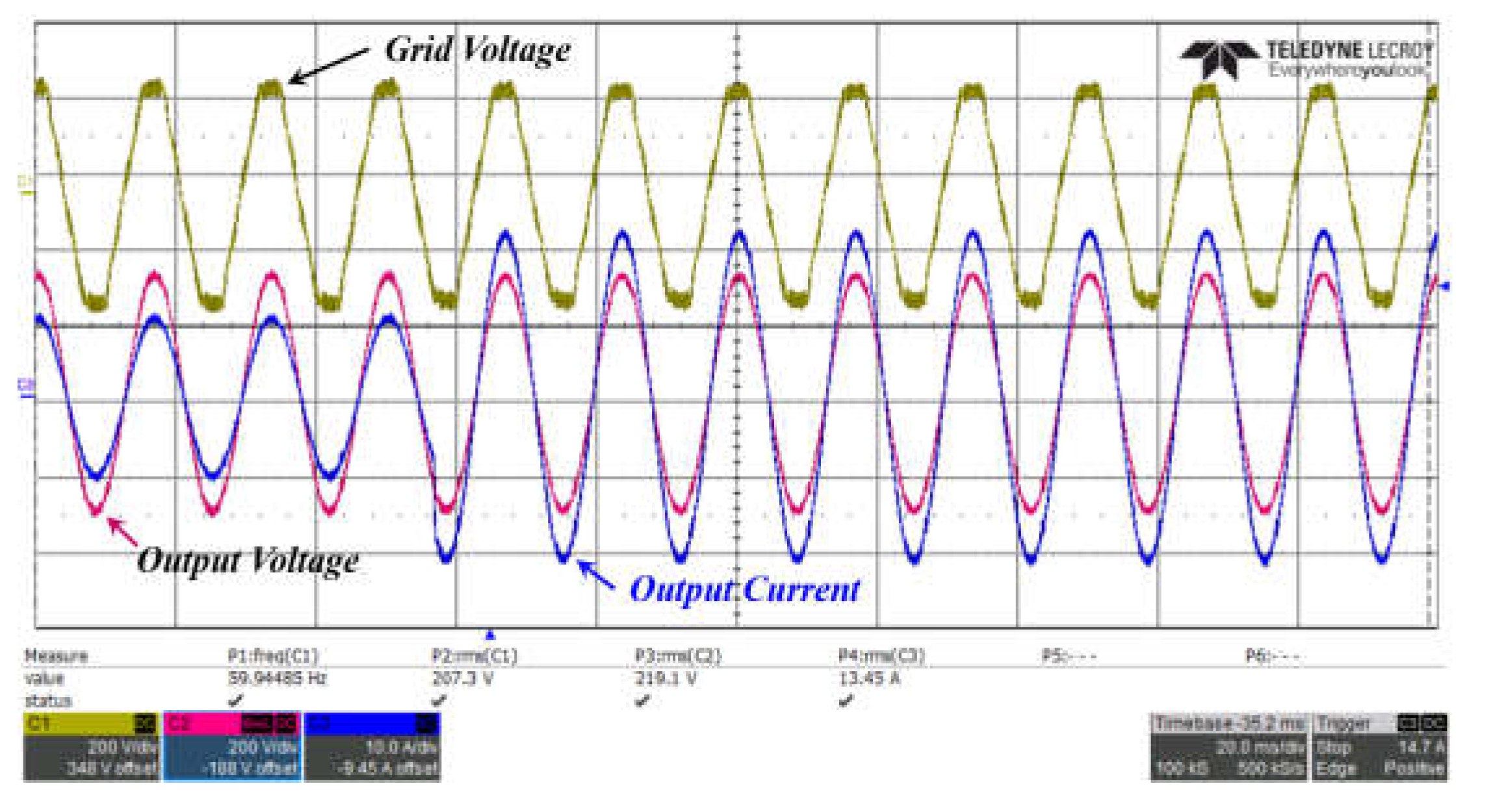
Figure 21.
Analysis of the voltage compensation waveforms in the DVR.
Disclaimer/Publisher’s Note: The statements, opinions and data contained in all publications are solely those of the individual author(s) and contributor(s) and not of MDPI and/or the editor(s). MDPI and/or the editor(s) disclaim responsibility for any injury to people or property resulting from any ideas, methods, instructions or products referred to in the content. |
© 2024 by the authors. Licensee MDPI, Basel, Switzerland. This article is an open access article distributed under the terms and conditions of the Creative Commons Attribution (CC BY) license (http://creativecommons.org/licenses/by/4.0/).
Copyright: This open access article is published under a Creative Commons CC BY 4.0 license, which permit the free download, distribution, and reuse, provided that the author and preprint are cited in any reuse.


