Submitted:
04 June 2024
Posted:
04 June 2024
You are already at the latest version
Abstract
Keywords:
1. Introduction
2. Piezoelectric Microphone Structure
2.1. Piezoelectric Layer
2.2. Mechanical Body
2.3. Acoustic Environment
3. Microphone Modeling
3.1. Finite-Elements Model
3.2. Lumped-Element Model
4. Parametric Optimization of the Microphone Structure
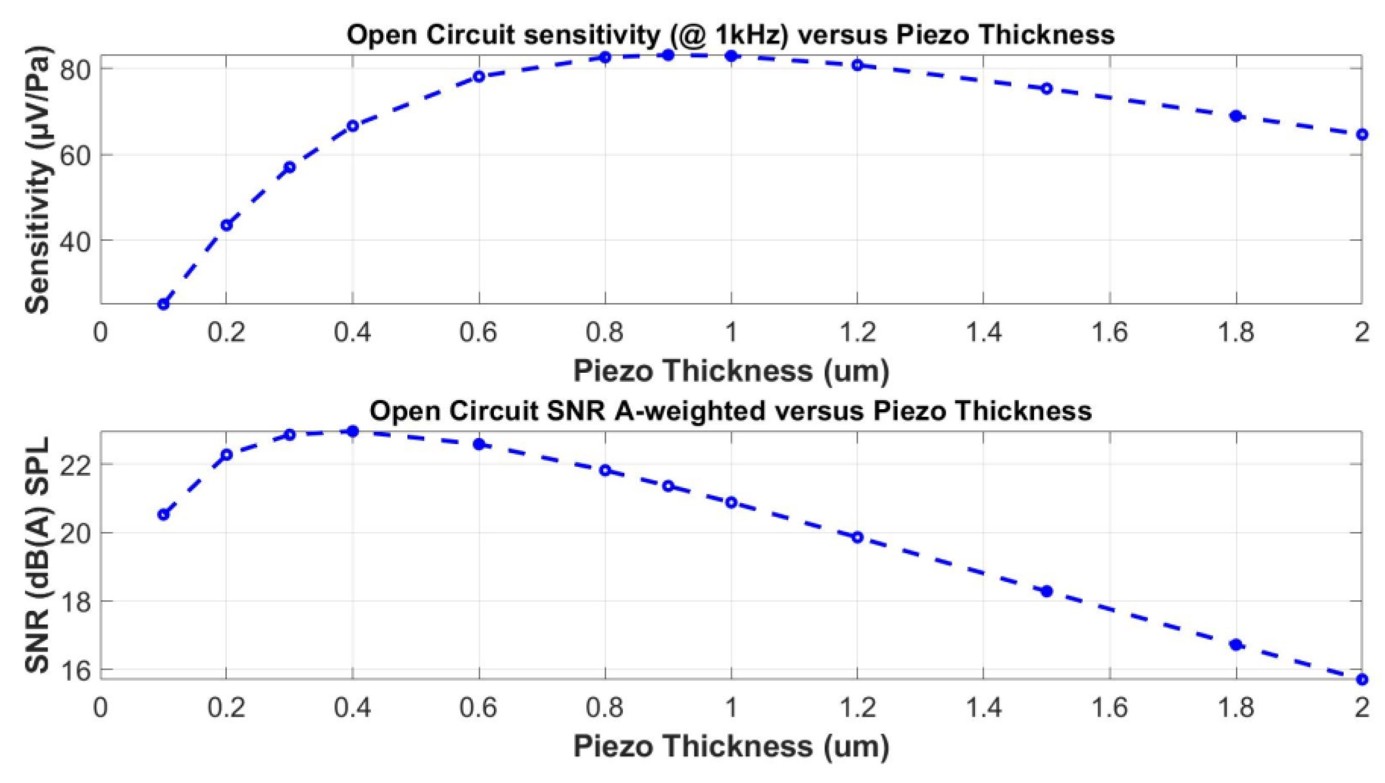
4.1. Optimization of the Piezoelectric Layer Thickness
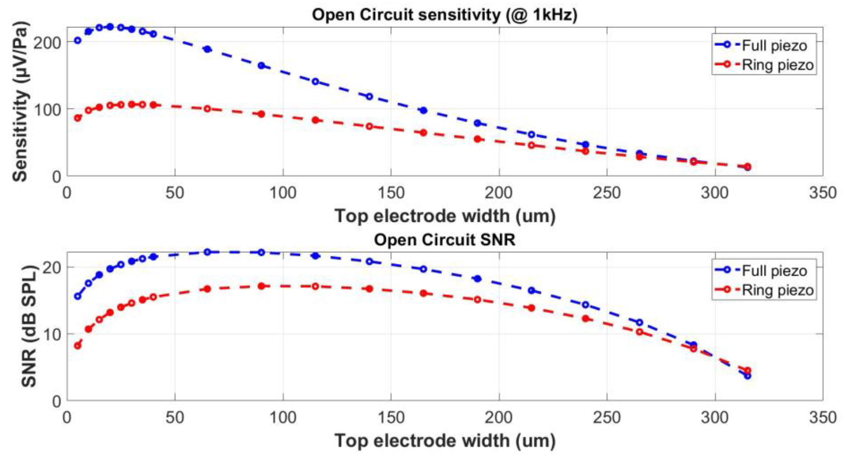
4.2. Optimization of the Piezoelectric Layer Width
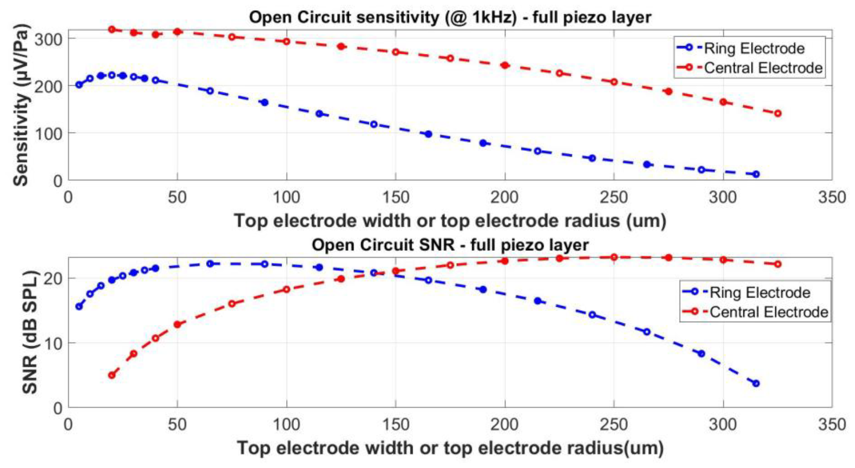
4.3. Effect of the Sensing Electrode Localization
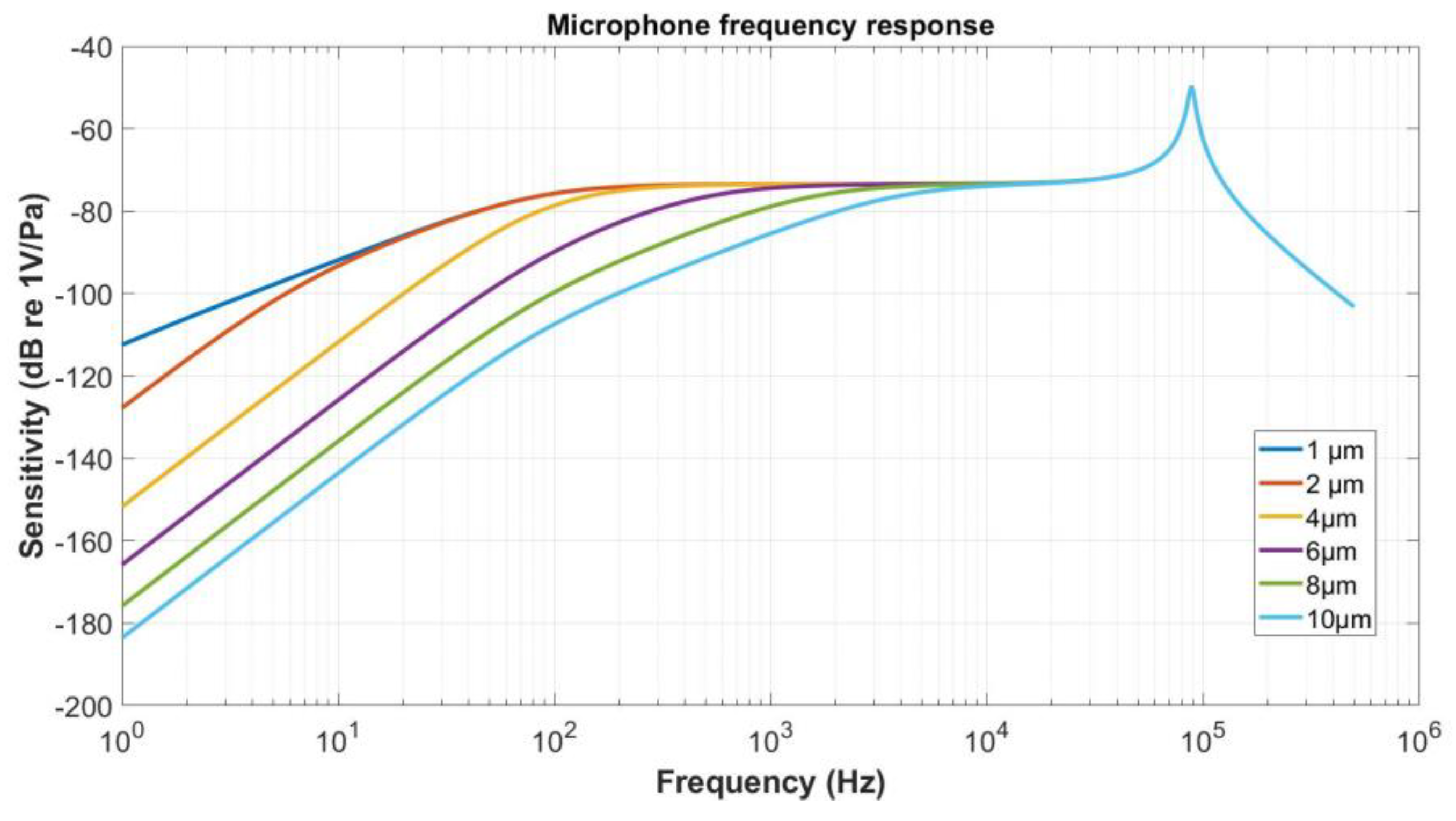
4.4. Effect of the Pressure Equalization Hole
4.5. Optimization Towards the Acoustic Overload Point
5. Microphone with Electrically Controlled Sensitivity
5.1. Basic Approach
5.2. Simulation Results
5. Conclusion
Author Contributions
Funding
Data Availability Statement
Conflicts of Interest
References
- Sessler, G.M.; West, J.E. Self-Biased Condenser Microphone with High Capacitance. Journal Acoust. Soc. Am. 1962, 34, 1787–1788. [Google Scholar] [CrossRef]
- Samaun, S.; Wise, K.D.; Nielsen, E.D.; Angel, J.B. An IC Piezoresistive Pressure Sensor for Biomedical Instrumentation. In Proceedings of the IEEE International Solid-state Circuits Conference; Univ. of Pennsylvania: USA, 1971; pp. 104–105. [Google Scholar] [CrossRef]
- Royer, M.; Holmen, P.; Wurm, M.; Aadland, P.; Glenn, M. ZnO on Si integrated acoustic sensor. Sensors & Actuators A Phys. 1983, 4, 357–362. [Google Scholar] [CrossRef]
- Hohm, D.; Sessler, G.M. An integrated silicon-electret-condenser microphone. In Proceedings of the 11th Int. Congress on Acoustics, Paris, France; 1983; pp. 29–32. [Google Scholar]
- Schellin, R.; Hess, G. A silicon subminiature microphone based on piezoresistive polysilicon strain gauges. Sensors & Actuators A Phys. 1992, 32, 555–559. [Google Scholar] [CrossRef]
- Kühnel, W. Silicon Condenser Microphone with Integrated Field-effect Transistor. Sensors & Actuators A Phys. 1991, 25–27, 521–525. [Google Scholar] [CrossRef]
- Schneider, U.; Schellin, R. A phase-modulating microphone utilizing integrated optics and micromachining in silicon. Sensors & Actuators A Phys. 1994, 41–42, 695–698. [Google Scholar] [CrossRef]
- Loeppert, P.V.; Lee, S.B. SiSonic TM—The First Commercialized MEMS Microphone. In Proceedings of the Solid-State Sensors, Actuators, and Microsystems Workshop, Hilton Head Island, South Carolina, USA; 2006; pp. 27–30. [Google Scholar] [CrossRef]
- Dehé, A.; Wurzer, M.; Füldner, M.; Krumbein, U. Design of a Poly Silicon MEMS Microphone for High Signal-to-Noise Ratio. In Proceedings of the European Solid-State Device Research Conference (ESSDERC), Bucharest, Romania; 2014; pp. 292–295. [Google Scholar] [CrossRef]
- Oralkan, O.; et al. Capacitive micromachined ultrasonic transducers: Next-generation arrays for acoustic imaging? IEEE Transactions on Ultrasonics, Ferroelectrics, and Frequency Control 2002, 49, 1596–1610. [Google Scholar] [CrossRef]
- Przybyla, R.J.; et al. In-Air Rangefinding With an AlN Piezoelectric Micromachined Ultrasound Transducer. IEEE Sensors Journal 2011, 11, 2690–2697. [Google Scholar] [CrossRef]
- Lu, Y.; Tang, H.; Fung, S.; Wang, Q.; Tsai, J.; Daneman, M.; Boser, B.; Horsley, D. Ultrasonic fingerprint sensor using a piezoelectric micromachined ultrasonic transducer array integrated with complementary metal oxide semiconductor electronics. Appl. Phys. Lett. 2015, 106, 5. [Google Scholar] [CrossRef]
- He, Q.; Liu, J.; Yang, B.; Wang, X.; Chen, X.; Yang, C. MEMS-based ultrasonic transducer as the receiver for wireless power supply of the implantable microdevices. Sensors & Actuators A Phys. 2014, 219, 65–72. [Google Scholar]
- Williams, M.D.; Griffin, B.A.; Reagan, T.N.; Underbrink, J.R.; Sheplak, M. An AlN MEMS Piezoelectric Microphone for Aeroacoustics Applications. J. of Microelectromechanical Systems 2012, 21, 270–283. [Google Scholar] [CrossRef]
- Yamashita, K.; Tomiyama, K.; Yoshikawa, K.; Noda, M.; Okuyama, M. Resonant Frequency Tuning of Piezoelectric Ultrasonic Microsensors by Bias Voltage Application to Extra Top-Electrodes on PZT Diaphragms. Ferroelectrics 2010, 408, 48–54. [Google Scholar] [CrossRef]
- Nastro, A.; Ferrari, M.; Rufer, L.; Basrour, S.; Ferrari, V. Piezoelectric MEMS Acoustic Transducer with Electrically-Tunable Resonant Frequency. Micromachines 2022, 13, 1–17. [Google Scholar] [CrossRef] [PubMed]
- Yamashita, K.; Shimizu, N.; Okuyama, M. Piezoelectric Charge Distribution on Vibrating Diaphragms with Static Deflection and Sensitivity Improvement of Ultrasonic Sensors. Journal of the Korean Physical Society, 2007, 51, 785–789. [Google Scholar] [CrossRef]
- Kanno, I. Piezoelectric MEMS: Ferroelectric Thin Films for MEMS Applications. Japanese Journal of Applied Physics 2018, 57, 1–9. [Google Scholar] [CrossRef]
- Muralt, P. Ferroelectric thin films for micro-sensors and actuators: A review. Journal of Micromechanics and Microengineering 2000, 10, 136–146. [Google Scholar] [CrossRef]
- Muralt, P. PZT Thin Films for Microsensors and Actuators: Where Do We Stand? IEEE Trans. on Ultrasonics, Ferroelectrics, and Frequency Control 2000, 47, 903–915. [Google Scholar] [CrossRef] [PubMed]
- Trolier-McKinstry, S.; Muralt, P. Thin Film Piezoelectrics for MEMS. Journal of Electroceramics 2004, 12, 7–17. [Google Scholar] [CrossRef]
- Ngoc Thao, P.; Yoshida, S.; Tanaka, S. Fabrication and Characterization of PZT Fibered-Epitaxial Thin Film on Si for Piezoelectric Micromachined Ultrasound Transducer. Micromachines 2018, 9, 1–22. [Google Scholar] [CrossRef]
- Gangidi, P.; Gupta, N. Optimal selection of dielectric film in piezoelectric MEMS microphone. Microsystem Technologies 2019, 25, 4227–4235. [Google Scholar] [CrossRef]
- Poudyal, A.; Jackson, N. Characterization of confocal sputtered molybdenum thin films for aluminum nitride growth. Thin Solid Films 2020, 693, 1–7. [Google Scholar] [CrossRef]
- Ali, W.R.; Prasad, M. Piezoelectric MEMS based acoustic sensors: A review. Sensors & Actuators A Phys. 2020, 301, 1–31. [Google Scholar]
- Dutta, S.; Pandey, A. Overview of residual stress in MEMS structures: Its origin, measurement, and control. J. of Mat. Sci.: Materials in Electronics 2021, 32, 6705–6741. [Google Scholar] [CrossRef]
- Yang, H.; Liu, M.; Zhu, Y.; Wang, W.; Qin, X.; He, L.; Jiang, K. Characterization of Residual Stress in SOI Wafers by Using MEMS Cantilever Beams. Micromachines 2023, 14, 1510. [Google Scholar] [CrossRef] [PubMed]
- Pandey, A.; Dutta, S.; Prakash, R.; Raman, R.; Kapoor, A.K.; Kaur, D. Growth and Comparison of Residual Stress of AlN Films on Silicon (100), (110) and (111) Substrates. Journal of Electronic Materials 2018, 47, 1405–1413. [Google Scholar] [CrossRef]
- Schlögl, M.; Weißenbach, J.; Schneider, M.; Schmid, U. Stress engineering of polycrystalline aluminum nitride thin films for strain sensing with resonant piezoelectric microbridges. Sensors & Actuators A Phys. 2023, 349, 1–11. [Google Scholar]
- Fazzio, R.S.; Lamers, T.; Buccafusca, O.; Goel, A.; Dauksher, W. Design and performance of aluminum nitride piezoelectric microphones. In Proceedings of the 14th International Solid-State Sensors, Actuators and Microsystems Conference, Lyon, France; 2007; pp. 1255–1258. [Google Scholar] [CrossRef]
- Merhaut, J. Theory of Electroacoustics; McGraw-Hill: New York, USA, 1981; 317p. [Google Scholar]
- Reutter, T.; Schrag, G. Reliable Piezoelectric FEM-Simulations of MEMS Microphones: Basis for Intrinsic Stress Reduction. In Proceedings of the IEEE Sensors Conference; 2010; pp. 193–196. [Google Scholar] [CrossRef]
- Esteves, J.; Rufer, L.; Ekeom, D.; Basrour, S. Lumped-parameters equivalent circuit for condenser microphones modeling. Journal Acoust. Soc. Am 2017, 142, 2121–2132. [Google Scholar] [CrossRef]
- Esteves, J.; Rufer, L.; Ekeom, D.; Defoort, M.; Basrour, S. Approaches to Piezoelectric Micromachined Microphone Design: Comparative Study. In Proceedings of the 10th Conv. of the European Acoustics Association, Forum Acusticum, Torino, Italy, 11–15th September 2023; pp. 4909–4916. [Google Scholar] [CrossRef]
- Timoshenko, P.; Krieger, S.W. Theory of Plates and Shells; McGraw-Hill: NY, USA, 1959. [Google Scholar]
- Wang, G.; Sankar, B.V.; Cattafesta, L.N.; Sheplak, M. Analysis of a Composite Piezoelectric Circular Plate With Initial Stresses for MEMS. In Proceedings of the IMECE, New Orleans, Louisiana, USA; 2002; pp. 1–8. [Google Scholar] [CrossRef]
- Yamashita, K.; Nishimoto, H.; Okuyama, M. Diaphragm deflection control of piezoelectric ultrasonic microsensors for sensitivity improvement. Sensors & Actuators A Phys. 2007, 139, 118–123. [Google Scholar] [CrossRef]



| Property | AlN | PZT |
|---|---|---|
| Compliance s11E [TPa-1] | 3.53 | 12.8 |
| Compliance s12E [TPa-1] | -1.01 | -3.7 |
| Compliance s13E [TPa-1] | -0.77 | -5.8 |
| Material density [kg/m3] | 3260 | 7700 |
| Piezoelectric constant d31[pm/V] | -2.65 | -118 |
| Piezoelectric constant e31[C/m2] | -0.58 | -4.1 |
| Relative permittivity ε33T [-] | 9.5 | 1160 |
| Dielectric loss angle (tanδ) [%] | 0.3 | 2 |
| Figure of merit MN [105 Pa1/2] | 20.9 | 9 |
| Property | Si | SiO2 | Al |
|---|---|---|---|
| Compliance s11E [TPa-1] | 7.67 | 13.7 | 14.3 |
| Compliance s12E [TPa-1] | -2.13 | -2.33 | -5 |
| Compliance s13E [TPa-1] | -2.13 | -2.33 | -5 |
| Material density [kg/m3] | 2330 | 2200 | 2700 |
Disclaimer/Publisher’s Note: The statements, opinions and data contained in all publications are solely those of the individual author(s) and contributor(s) and not of MDPI and/or the editor(s). MDPI and/or the editor(s) disclaim responsibility for any injury to people or property resulting from any ideas, methods, instructions or products referred to in the content. |
© 2024 by the authors. Licensee MDPI, Basel, Switzerland. This article is an open access article distributed under the terms and conditions of the Creative Commons Attribution (CC BY) license (http://creativecommons.org/licenses/by/4.0/).


