Submitted:
05 June 2024
Posted:
06 June 2024
You are already at the latest version
Abstract
Keywords:
1. Introduction
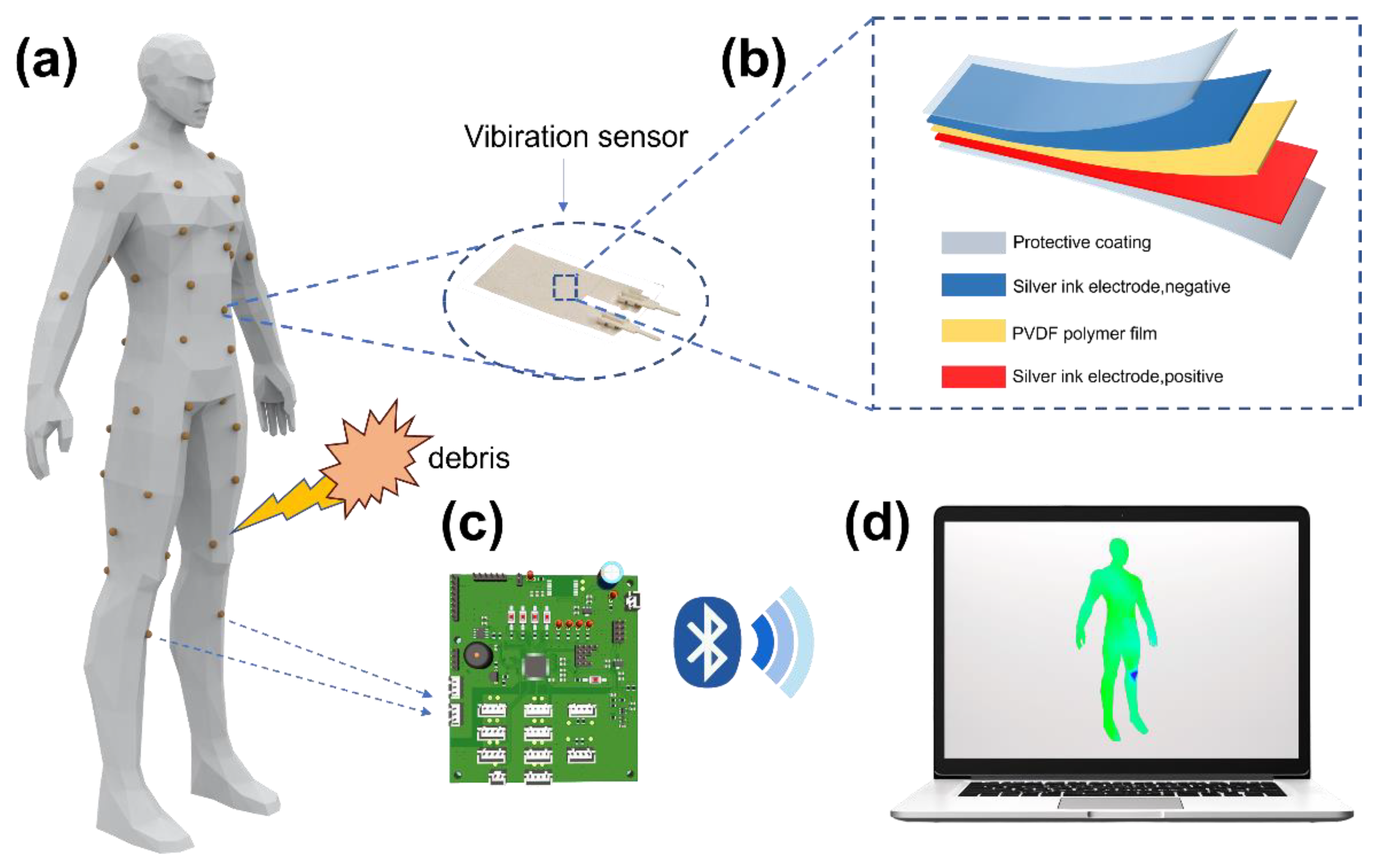
2. System Design
2.1. Piezoelectric Sensor Selection and Structural Analysis
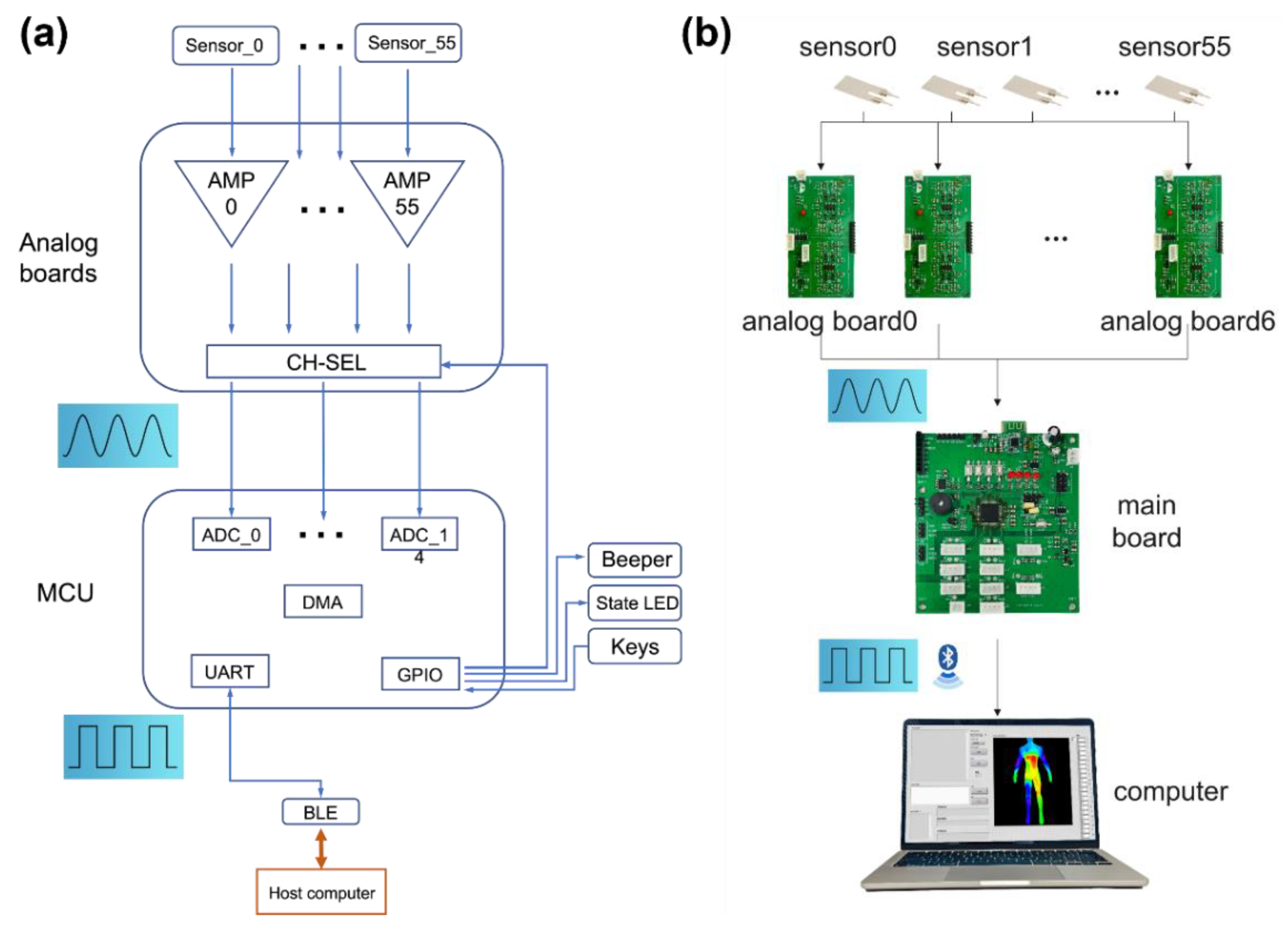
2.2. Hardware Circuit
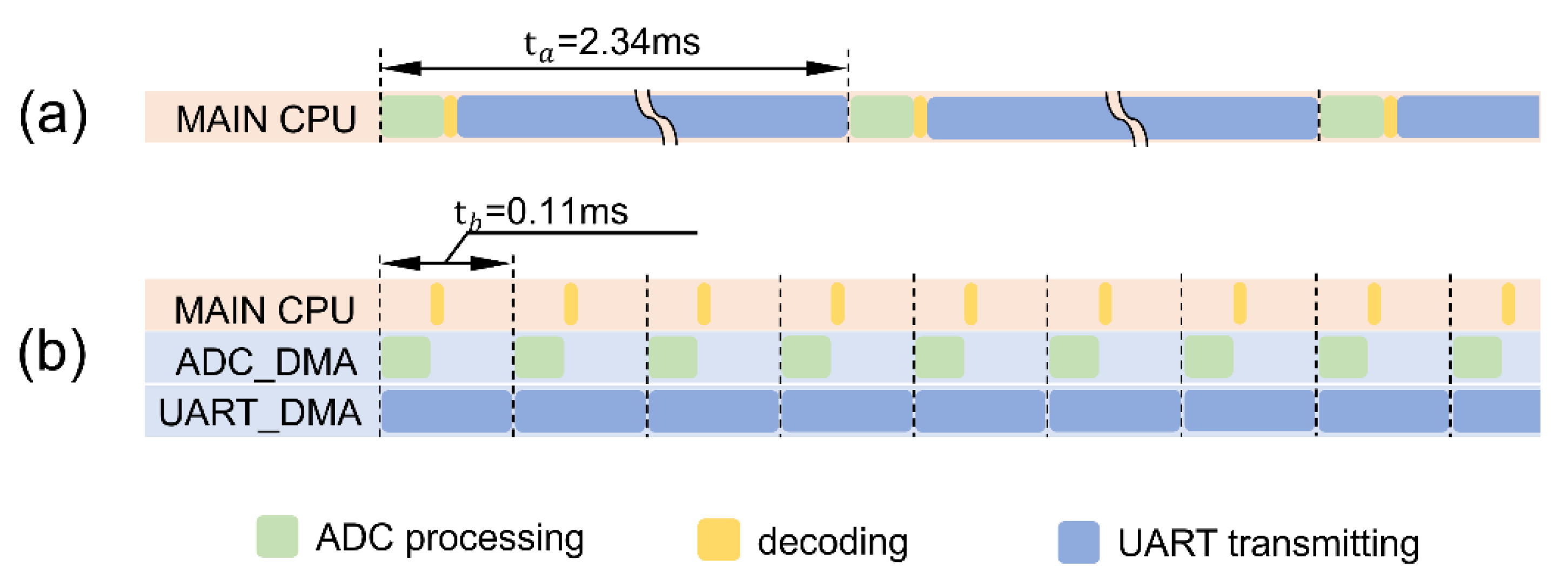
2.3. Software Program
2.4. State Machine Partitioning
2.4.1. Init State
2.4.2. Wait State
- Serial_Open Button: If the port is closed, sets the port name and baud rate, opens the port, and moves to GetData state. If open, closes the port and stays in Wait.
- Clear Button: Resets all arrays to zero. If the port is open, proceeds to GetData; if closed, remains in Wait.
- Exit Button: Transitions to Exit state, closing the serial port and terminating the LabVIEW program if open, or exits directly if the port is already closed.
2.4.3. GetData State
2.4.4. Exit State
2.5. Data Decoding
2.6. Error Data Handling
2.7. Three-Dimensional Model Visualization Post-Data Decoding
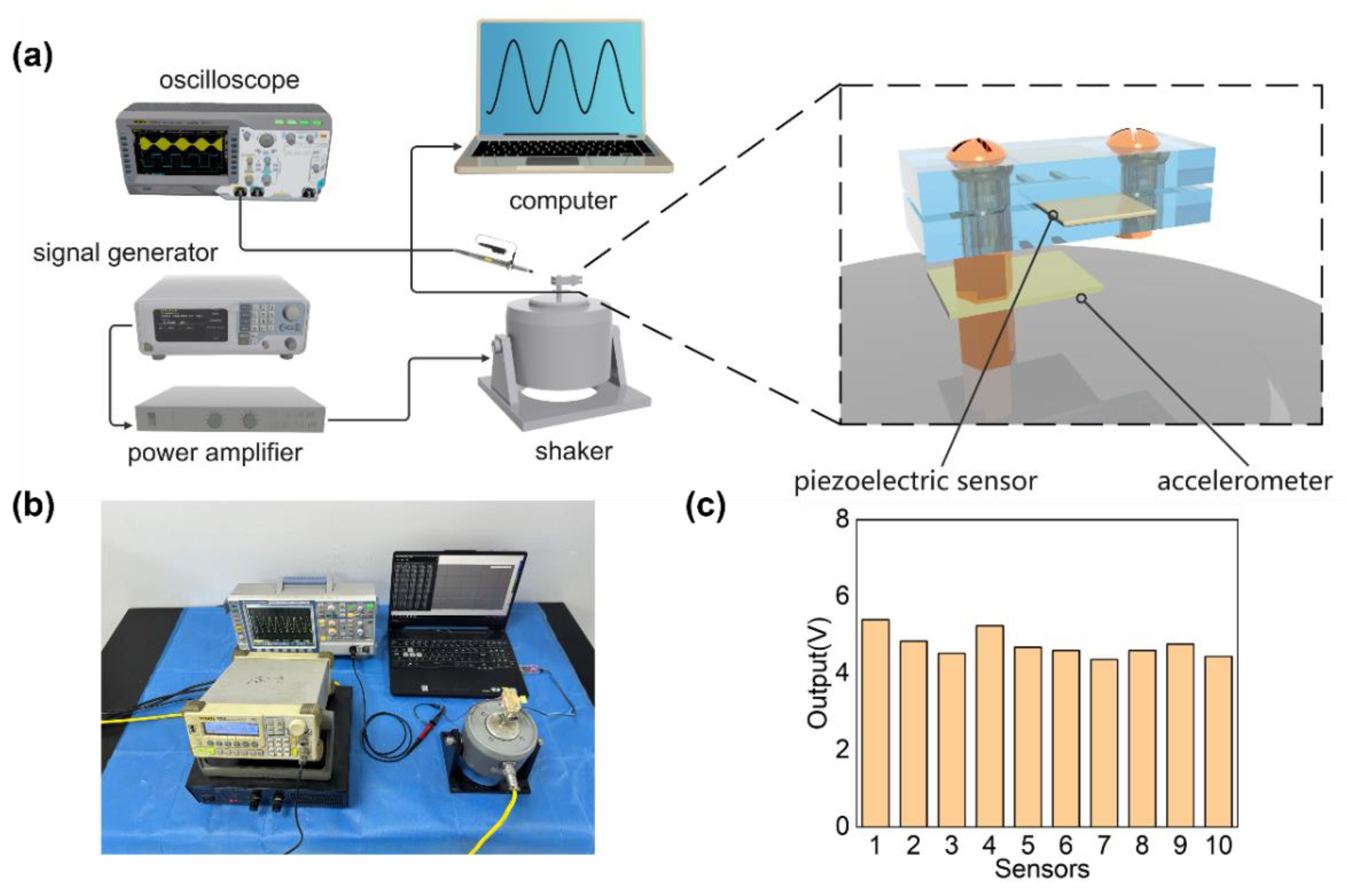
3. Results and Discussion
Author Contributions
Funding
Institutional Review Board Statement
Informed Consent Statement
Data Availability Statement
Conflicts of Interest
References
- Park, H.; Park, J.; Lin, S.-H.; Boorady, L.M. Assessment of Firefighters’ needs for personal protective equipment. Fashion and Textiles 2014, 1, 1–13. [Google Scholar] [CrossRef]
- Jin, Q.; Tan, S.; Zhang, G.; Yang, Z.; Wen, Y.; Xiao, H.; Wu, X. Visible and Infrared Image Fusion of Forest Fire Scenes Based on Generative Adversarial Networks with Multi-Classification and Multi-Level Constraints. Forests 2023, 14, 1952. [Google Scholar] [CrossRef]
- Raimundo, A.M.; Figueiredo, A.R. Personal protective clothing and safety of firefighters near a high intensity fire front. Fire Safety Journal 2009, 44, 514–521. [Google Scholar] [CrossRef]
- Monea, B.F.; Ionete, E.I.; Spiridon, S.I.; Ion-Ebrasu, D.; Petre, E. Carbon nanotubes and carbon nanotube structures used for temperature measurement. Sensors 2019, 19, 2464. [Google Scholar] [CrossRef]
- Kane, C.; Mele, E.; Lee, R.; Fischer, J.; Petit, P.; Dai, H.; Thess, A.; Smalley, R.; Verschueren, A.; Tans, S. Temperature-dependent resistivity of single-wall carbon nanotubes. Europhysics Letters 1998, 41, 683. [Google Scholar] [CrossRef]
- Wang, Y.; Liu, J.; Zhao, Y.; Qin, Y.; Zhu, Z.; Yu, Z.; He, H. Temperature-triggered fire warning PEG@ wood powder/carbon nanotube/calcium alginate composite aerogel and the application for firefighting clothing. Composites Part B: Engineering 2022, 247, 110348. [Google Scholar] [CrossRef]
- Baksi, A.; Bhattacharjee, M.; Ghosh, S.; Bishnu, S.K.; Chakraborty, A. Internet of Things (IOT) based ambulance tracking system using GPS and GSM modules. In Proceedings of the 2020 4th International Conference on Electronics, Materials Engineering & Nano-Technology (IEMENTech), 2020. pp. 1–4,.
- Pettorru, G.; Pilloni, V.; Martalò, M. Trustworthy Localization in IoT Networks: A Survey of Localization Techniques, Threats, and Mitigation. Sensors 2024, 24, 2214. [Google Scholar] [CrossRef]
- Blecha, T.; Soukup, R.; Kaspar, P.; Hamacek, A.; Reboun, J. Smart firefighter protective suit-functional blocks and technologies. In Proceedings of the 2018 IEEE International Conference on Semiconductor Electronics (ICSE), 2018. pp. C4–C4.
- Vallozzi, L.; Vandendriessche, W.; Rogier, H.; Hertleer, C.; Scarpello, M. Design of a protective garment GPS antenna. Microwave and optical technology letters 2009, 51, 1504–1508. [Google Scholar] [CrossRef]
- Li, Y.; Liu, C.; Zou, H.; Che, L.; Sun, P.; Yan, J.; Liu, W.; Xu, Z.; Yang, W.; Dong, L. Integrated wearable smart sensor system for real-time multi-parameter respiration health monitoring. Cell Reports Physical Science 2023, 4, 1–9. [Google Scholar] [CrossRef]
- Bruce-Low, S.; Cotterrell, D.; Jones, G. Effect of wearing personal protective clothing and self-contained breathing apparatus on heart rate, temperature and oxygen consumption during stepping exercise and live fire training exercises. Ergonomics 2007, 50, 80–98. [Google Scholar] [CrossRef]
- Tochihara, Y.; Lee, J.-Y.; Son, S.-Y. A review of test methods for evaluating mobility of firefighters wearing personal protective equipment. Industrial health 2022, 60, 106–120. [Google Scholar] [CrossRef] [PubMed]
- Liu, C.; Wang, Y.; Zhang, N.; Yang, X.; Wang, Z.; Zhao, L.; Yang, W.; Dong, L.; Che, L.; Wang, G. A self-powered and high sensitivity acceleration sensor with VQa model based on triboelectric nanogenerators (TENGs). Nano Energy 2020, 67, 104228. [Google Scholar] [CrossRef]
- Liu, C.; Fang, L.; Zou, H.; Wang, Y.; Chi, J.; Che, L.; Zhou, X.; Wang, Z.; Wang, T.; Dong, L. Theoretical investigation and experimental verification of the self-powered acceleration sensor based on triboelectric nanogenerators (TENGs). Extreme Mechanics Letters 2021, 42, 101021. [Google Scholar] [CrossRef]
- Kester, W. Which ADC architecture is right for your application. In Proceedings of the EDA Tech Forum, 2005. pp. 22–25.
- Dan, S.; Yano, Y.; Wang, J. Batteryless BLE Module with a Piezoelectric Element Mounted on a Shoe Sole. Sensors 2024, 24, 2829. [Google Scholar] [CrossRef] [PubMed]
- Decharat, A.; Wagle, S.; Jacobsen, S.; Melandsø, F. Using Silver Nano-Particle Ink in Electrode Fabrication of High Frequency Copolymer Ultrasonic Transducers: Modeling and Experimental Investigation. Sensors 2015, 15, 9210–9227. [Google Scholar] [CrossRef] [PubMed]
- Gandelli, A.; Ottoboni, R. Charge amplifiers for piezoelectric sensors. In Proceedings of the 1993 IEEE Instrumentation and Measurement Technology Conference, 1993. pp. 465–468.
- Han, S.-J.; Jenkins, K.A.; Valdes Garcia, A.; Franklin, A.D.; Bol, A.A.; Haensch, W. High-frequency graphene voltage amplifier. Nano letters 2011, 11, 3690–3693. [Google Scholar] [CrossRef]
- Qiu, Y.; Shi, L.; Chen, L.; Yu, Y.; Yu, G.; Zhu, M.; Zhou, H. A Wide-Band Magnetoelectric Sensor Based on a Negative-Feedback Compensated Readout Circuit. Sensors 2024, 24, 423. [Google Scholar] [CrossRef]
- Shen, H.; Zhu, Z.; Lu, H.; Ju, H.; Huang, J.; Chen, Z. Development of a Sandwiched Piezoelectric Accelerometer for Low-Frequency and Wide-Band Seismic Exploration. Sensors 2023, 23, 9168. [Google Scholar] [CrossRef] [PubMed]
- Pinna, L.; Valle, M. Charge amplifier design methodology for PVDF-based tactile sensors. Journal of Circuits, Systems and Computers 2013, 22, 1350066. [Google Scholar] [CrossRef]
- Alnasser, E. A novel low output offset voltage charge amplifier for piezoelectric sensors. IEEE Sensors Journal 2020, 20, 5360–5367. [Google Scholar] [CrossRef]
- Kodosky, J. LabVIEW. Proceedings of the ACM on Programming Languages 2020, 4, 1–54. [Google Scholar] [CrossRef]
- Yang, B.; Guo, Y.; Wang, Z.D.; Gao, Y. Serial communication based on LabVIEW for the development of an ECG monitor. Advanced Materials Research 2013, 734, 3003–3006. [Google Scholar] [CrossRef]
- Lin, J.Q.; Xia, M.H.; Yang, W.L.; Leng, J. Design of Labview based equipment for measuring Thermally Stimulated Current. Applied Mechanics and Materials 2013, 274, 555–558. [Google Scholar] [CrossRef]
- Machacek, J.; Drapela, J. Control of serial port (RS-232) communication in LabVIEW. In Proceedings of the 2008 International Conference-Modern Technique and Technologies, 2008. pp. 36–40.
- Win, M.T. Comparison Between Mealy and Moore State Models UsingSequence Detector with VHDL Coding Techniques. International Journal of Advanced Research in Computer Engineering & Technology (IJARCET) 2018, 7, 651–656. [Google Scholar]
- Nedjah, N.; Mourelle, L.d.M. Mealy finite state machines: An evolutionary approach. International Journal of Innovative Computing, Information and Control 2006, 2, 789–806. [Google Scholar]
Disclaimer/Publisher’s Note: The statements, opinions and data contained in all publications are solely those of the individual author(s) and contributor(s) and not of MDPI and/or the editor(s). MDPI and/or the editor(s) disclaim responsibility for any injury to people or property resulting from any ideas, methods, instructions or products referred to in the content. |
© 2024 by the authors. Licensee MDPI, Basel, Switzerland. This article is an open access article distributed under the terms and conditions of the Creative Commons Attribution (CC BY) license (http://creativecommons.org/licenses/by/4.0/).


