1. Introduction
The response and performance of sensor devices are critically influenced by several factors, including the size, shape, and surface characteristics of the active oxide material. These attributes play a crucial role in defining the electronic and optical properties of oxides, which are known to vary significantly with spatial dimensions and composition. Among the various forms that these materials can take, thin films have emerged as one of the most effective configurations for achieving high sensitivity in sensors. This heightened sensitivity is primarily due to the increased number of surface atoms present in thin films, which enhances their interaction with the surrounding environment. The physical and chemical properties of the nano-structured sensing layer, such as tungsten oxide (WO3), are notably different from those of their bulk counterparts. This disparity arises because the large surface area to volume ratio in nanostructures intensifies surface effects. In nano-scale dimensions, the effective van der Waals forces, Coulombic interactions, and inter-atomic couplings are significantly altered compared to the bulk material. These modified interactions lead to changes in the electronic structure and chemical reactivity of the material. Specifically, the high surface area in thin films means that a larger proportion of the atoms are exposed to the environment, which can enhance the sensitivity of the sensor. The increased surface interactions enable the material to respond more readily to external stimuli, such as changes in gas concentration, temperature, or light. Furthermore, the reduced dimensionality in thin films can result in quantum confinement effects, which can further modify the electronic properties of the material, leading to improved performance in applications like gas sensing, photodetectors, and other optoelectronic devices. The ability to tailor the properties of the oxide material by manipulating its size, shape, and surface characteristics opens new possibilities for designing sensors with enhanced performance. For example, by optimizing the thickness of WO3 thin films and controlling their nanostructure, it is possible to achieve a balance between high sensitivity and stability, which is crucial for practical sensor applications. The interplay between surface atoms and the altered inter-atomic forces in these nanostructured films provides a rich field of study for developing advanced materials with superior sensing capabilities. The performance of sensor devices is intricately linked to the characteristics of the active oxide material, particularly in its nano-structured thin film form. The unique properties that arise from the high surface area and modified inter-atomic interactions in these materials pave the way for highly sensitive and efficient sensors, making thin films a preferred choice in the design of next-generation sensing technologies.
WO
3 is a typical n-type gas-sensing material that attracted considerable attention and it is used to detect various hazardous gases. Previous studies indicated that unique nanostructuring during growth is highly related to the sensing performances. Countless advances have been achieved to design and fabricate diverse WO
3 in different forms. However, it is still challenging to achieve high performances. To significantly enhance the gas-sensing properties, many strategies have been explored. Although the mechanisms responsible for WO
3 gas sensing are not completely understood, an empirical model to explain the fundamental gas sensing mechanism is widely accepted as follows. Upon exposing to air, oxygen molecules will be chemisorbed on the WO
3 surface, inducing the creation of an electron depletion layer by attracting electrons from conduction band. The adsorbed oxygen can further evolve into active oxygen species such as O
2−, O−, and O
2− at a certain temperature [
2], which is highly reactive with target gas molecules. The charge carriers are affected by the presence of target gas. For example, a reduction reaction can occur between reducing gases and these oxygen species, leading to the release of the trapped electrons back. As a result, the change in resistance reflects the concentrations of target gas. In the past years, typical 2D WO
3 structures such as thin films have drawn considerable attention in the gas-sensing field due to the high surface-to-volume ratio, modulated surface activities, surface polarization and rich oxygen vacancies. Many studies on WO
3 use as sensing layers are present in the scientific literature but this material is still challenging [
3,
4]. Raman spectroscopy can detect different stoichiometries and structures, including polymorphs that contain the same atoms but in different crystalline forms. This technique allows for the analysis of mixtures and the quantification of their chemical composition. Despite the extensive research on WO
3 thin films, a Raman spectroscopy study examining the effects of thickness variations correlated with the initial concentration of the precursor has, to our knowledge, not been performed before. This specific investigation is important as it could provide new insights into how these variables influence the material's structural and chemical properties, which are critical for optimizing its performance in various applications. By leveraging Raman spectroscopy, one can detect subtle changes in the WO
3 thin films' structure and composition induced by varying thickness and precursor concentration. This method's sensitivity to different stoichiometries and crystalline forms makes it particularly suited for such an analysis. Therefore, conducting this study could potentially uncover novel information about the interplay between film thickness, precursor concentration, and the resultant properties of WO
3 thin films. This could lead to improved methodologies for fabricating thin films with tailored properties for specific technological applications. The scope of the present study is to observe and correlate structural properties characterized by Raman spectroscopy for two kinds of pure WO
3 nanostructured thin films thickness series grown from precursors with two different concentrations leading to a rare structuring of the surface, only briefly noticed in the scientific literature. As mentioned above, up to our knowdlege, a Raman spectroscopy study of the thickness variations effect correlated with initial concentration of precursor was never performed before on WO
3 thin films. This is a specific niche in materials science research. While WO
3 thin films and their properties have been extensively studied, the unique combination of variables—thickness variation and initial precursor concentration, specifically analyzed through Raman spectroscopy is novel.
3. Results and Discussions
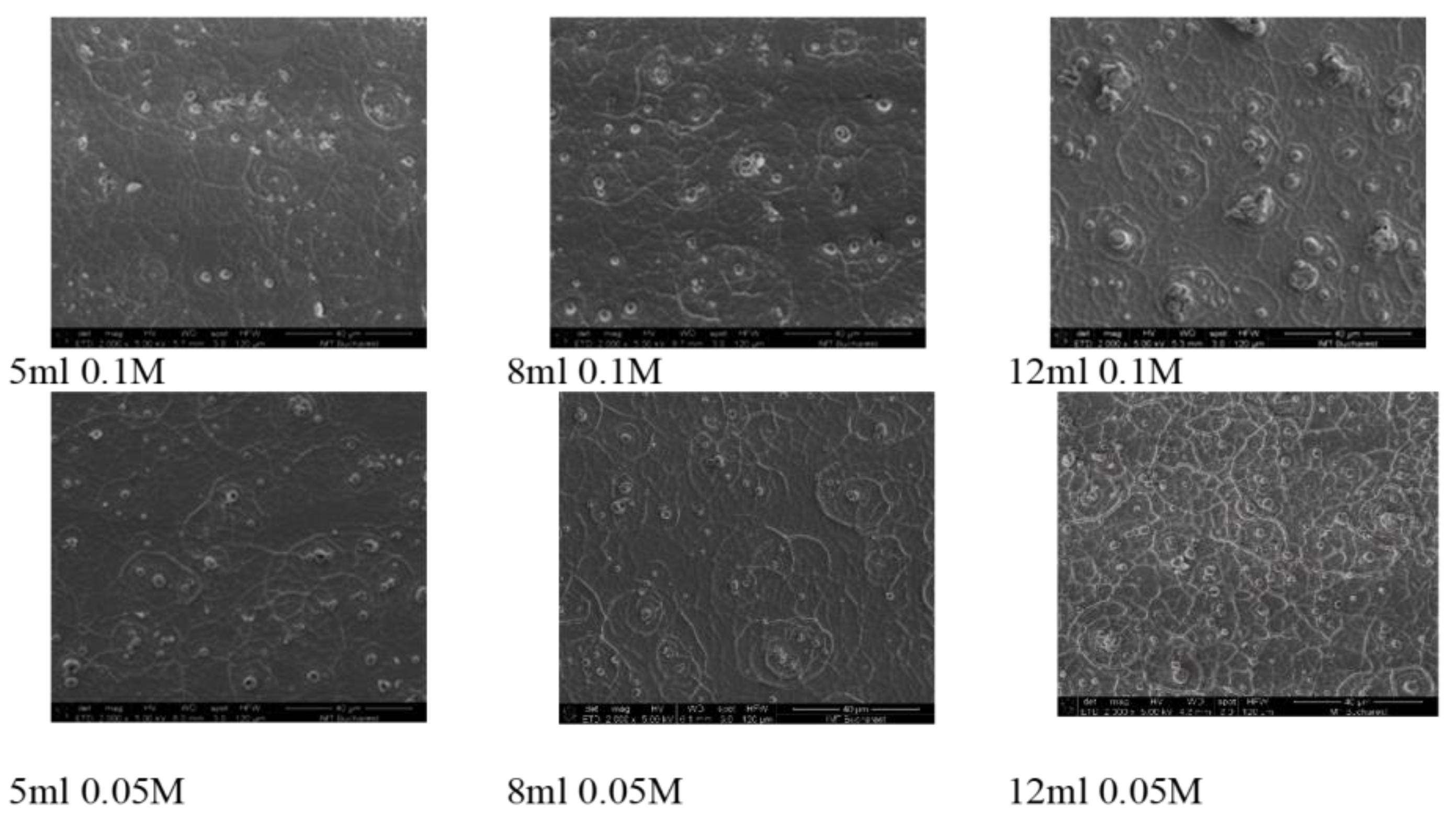
SEM imaging at low-magnification was conducted on six samples selected upon the precursor’s volumes and concentrations: 5, 8, 12 ml at 0.1 M and 0.05 M. The SE images displayed in Figure 1 disclose significant morphological variations on large areas of the WO3 layer, as seen below:
Figure 1.
SEM images of WO3 thin films grown at precursor’s volumes and concentrations: 5, 8, 12 ml at 0.1 M and 0.05 M.
Figure 1.
SEM images of WO3 thin films grown at precursor’s volumes and concentrations: 5, 8, 12 ml at 0.1 M and 0.05 M.
It can be observed that for a specific precursor concentration, the increasing thickness leads to a surface morphology with increased number of features. It is observed the presence of small islands alternating with walls like structures with size increasing as the thickness increases. With respect to the precursor concentration, higher molar concentration for the precursor solution leads to similar surface morphology at small thickness but, as the thickness increases the surface morphologies changes and, at lower precursor concentration a higher number of wall-like structures appears while the island like structures number and size decreases. At higher precursor concentration, the surface morphology seems to evolve towards larger islands-like structures as the thickness is increasing.
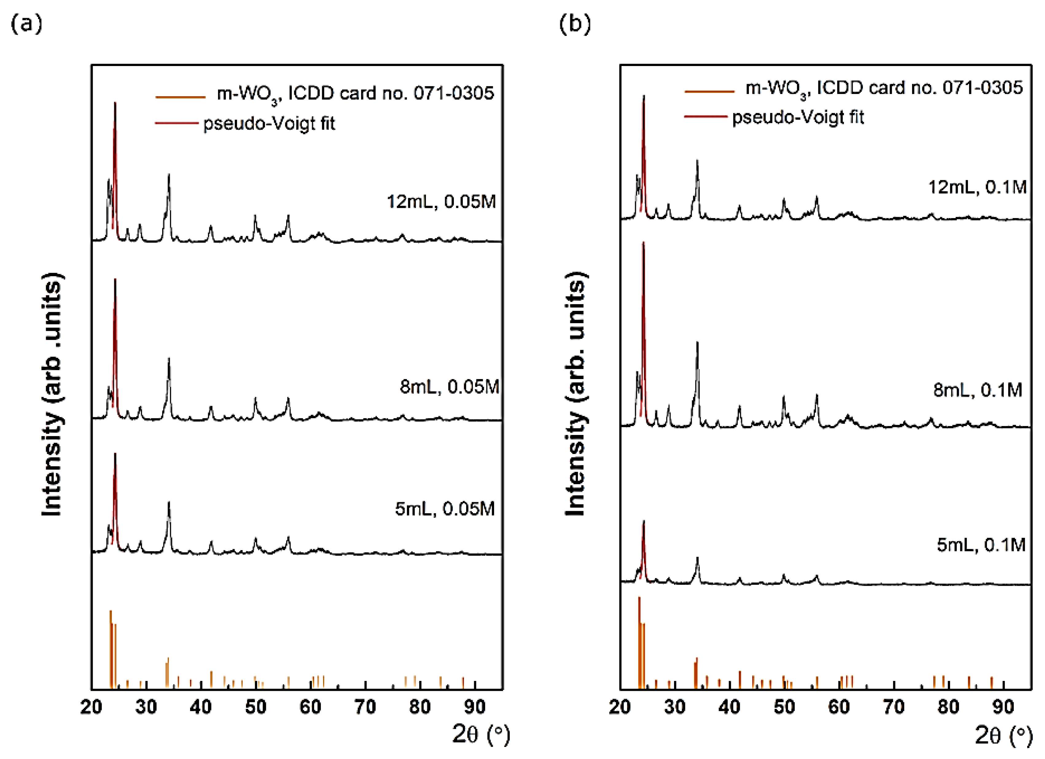
Grazing incidence X-ray diffraction was employed to study the constituent phases of WO
3 films. For this purpose, the incidence angle was kept at 0.5°, while the detector scanned in the 2θ range of 20 - 60° as shown in
Figure 2.
The XRD data reveal the presence of single phase WO
3. Each diffraction pattern presents a set of diffraction features with different intensities located at 23.1, 23.5, 24.2, 26.5, 28.7, 33.3, 34.1, 35.4, 41.7, 44.4, 45.6, 47.2, 48.3, 49.9, 50.7 and 55.8°, assigned with different (hkl) Miller indices using ICDD database – International Center for Diffraction Data. These were at-tributed to WO
3 with monoclinic crystal structure, belonging to P21/n(14) space group with the following lattice parameters and angles: a = 0.73 nm; b = 0.75 nm; c = 0.76 nm; α = 90°; β = 90.9°; γ = 90°, according to card no. 05-0363. No impurities peaks were detected in the XRD patterns. A monoclinic phase was also observed by different authors. For in-stance, Dongale and co-workers [
5] reported monoclinic WO
3 films obtained using spray pyrolysis at different substrate temperatures. Acosta et al. [
6] reported monoclinic phase of WO3 with a preferred orientation of the crystallites along the c-axis, while Ortega et al. [
7] showed the hexagonal and monoclinic phase co-existence on glass substrate and a pure monoclinic phase on FTO for WO
3 deposited by pulsed spray pyrolysis. In addition, multiple reports related to the WO
3 films and nanostructures exhibit monoclinic crystal structures [8; 9; 10]. Different deposition parameters do not affect the position of the diffraction peaks, which indicates that the interplanar distance of the monoclinic-WO3 remains constant along different precursor’s volume and concentration. However, the fitting of the main diffraction peaks located at 24.3˚, with a pseudo-Voigt function indicates that the crystal quality is affected at different deposition parameters. For instance, at 0.05M for the lowest precursor’s volume (5mL), the Full Width at Half Maximum (FWHM) of the main diffraction peak is 0.51˚. Further, when the precursor’s volume increases, the FWHM de-creases to 0.46˚ (8 mL), reaching to 0.45˚ (12 mL). Similarly, at 0.1 M, the FWHM decreases from 0.51˚ (5 mL) to 0.43˚ (8 and 12 mL). According to Scherrer equation [
11], with increasing the precursor’s volume, the crystal quality becomes better, which it is reflected in the mean crystallite size increases from ~ 16 nm to ~ 19.5 nm. These observations are sup-ported by the Raman spectroscopy characterization that follows.
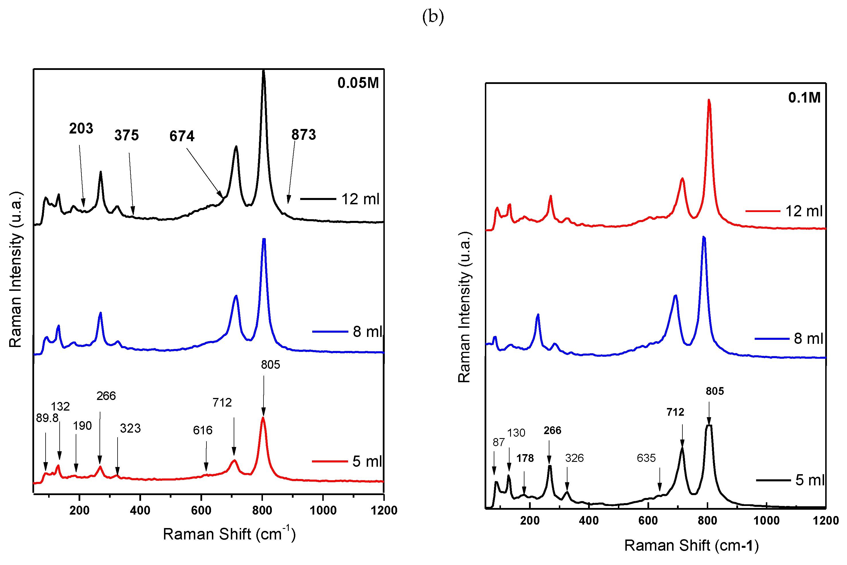
Raman spectroscopy results for the WO3 thin films grown at precursor’s volumes and concentrations: 5, 8, 12 ml at 0.1 M and 0.05 M are presented in
Figure 3.
As already mentioned, Raman spectroscopy offers important information about the crystalline phases of WO
3 crystal. Tungsten trioxide thin films can exist in different phases depending on synthesis temperature (a) low-temperature phase (m-WO
3) - this is the most stable phase of WO
3 at ambient conditions corresponding to the monoclinic crystal structure. The α-phase can be synthesized at relatively low temperatures, typically below 740°C [
12]; (b) high-temperature phase (- at higher temperatures, typically above 740°C, α-WO
3 transforms into the c-phase a cubic (ideal) crystal structure; (c) the phase transitions in the WO
3 thin films occur in sequence as the temperature is increased: monoclinic (α-WO
3) --> orthorhombic (β-WO
3) --> tetragonal phase (α-WO
3) [
13].
For sensing functions, the WO
3 needs to be nanostructured and have a large surface area to enable the analytes to diffuse through the film. Acentric nature and spontaneous electric dipole moment of ferroelectric ε–WO
3 for example, leads to increased interaction with high dipole moment analytes such as acetone [
14] which is used for medical devices sensing the acetone level in human breath in concentrations of parts per billion (ppb) for non–invasive blood glucose monitoring [
15]. In the monoclinic phase, photo electrochemical and photo catalytic properties are enhanced when the film is highly crystalline and preferentially oriented because this highly crystalline structure will have fewer defects when acting as the recombination center and should suppress mutual e––h+ recombination [
16]. According to some authors, polycrystalline WO
3 film has almost no photochromic sensitivity whereas amorphous WO
3 has high photochromic and electrochromic sensitivity due to high surface area [
17].
The fundamental Raman vibrational modes within the lattice of WO3 contain stretching (ν), bending (δ), and out-of-plane wagging (γ) modes.
In the monoclinic m-WO3 crystalline structure, these vibration modes are observed at ≃ 803, 714, and 270 cm
−1, corresponding to the stretching of ν (O−W−O) bonds, stretching of ν (W−O) bonds, and bending of δ (O−W−O) bonds, respectively [
18].
Comparing the Raman spectra (
Figure 3) obtained for WO
3 films made by spray deposition method with results reported in the literature using other deposition techniques (Chemical Vapor Deposition, Chemical Solution Deposition, or Dip-Coating), one can observe a dominant presence of vibration modes at 270 cm
-1, 714 cm
-1, and 805 cm
-1. This indicates a monoclinic structure of m-WO
3 but with changes in the Raman spectrum of the resulting material induced by the deposition method.
The O-W-O and W-O bonds in monoclinic structure remain unchanged, with variations only in intensity when the increase in volume for spray-coating (for 0.5 M δ (O-W-O), I12 ml/I5ml= 1.96) and are less sensitive to higher molar masses (for 0.1 M δ (O-W-O), I12 ml/I5ml = 0.15).
The WO
3 Raman spectra (
Figure 3a – 0.05 M probes) displays bands at low wavenumbers, observed within the wavenumber range of 80 - 400 cm
−1. Above all,
Figure 3b – 0.1 M probe with bands identification, there is a cluster of bands at 89,131, 190, and 266 cm
−1. The bands below 270 cm−1 are attributed to low frequency phonon charge marker. The band at 266 cm
−1 is attributed to lattice modes ν (O-W-O) vibration, the other bands correspond to W-W lattice modes vibration. At the same time, the Raman bands corresponding to the W-W bonding located in the 200 cm
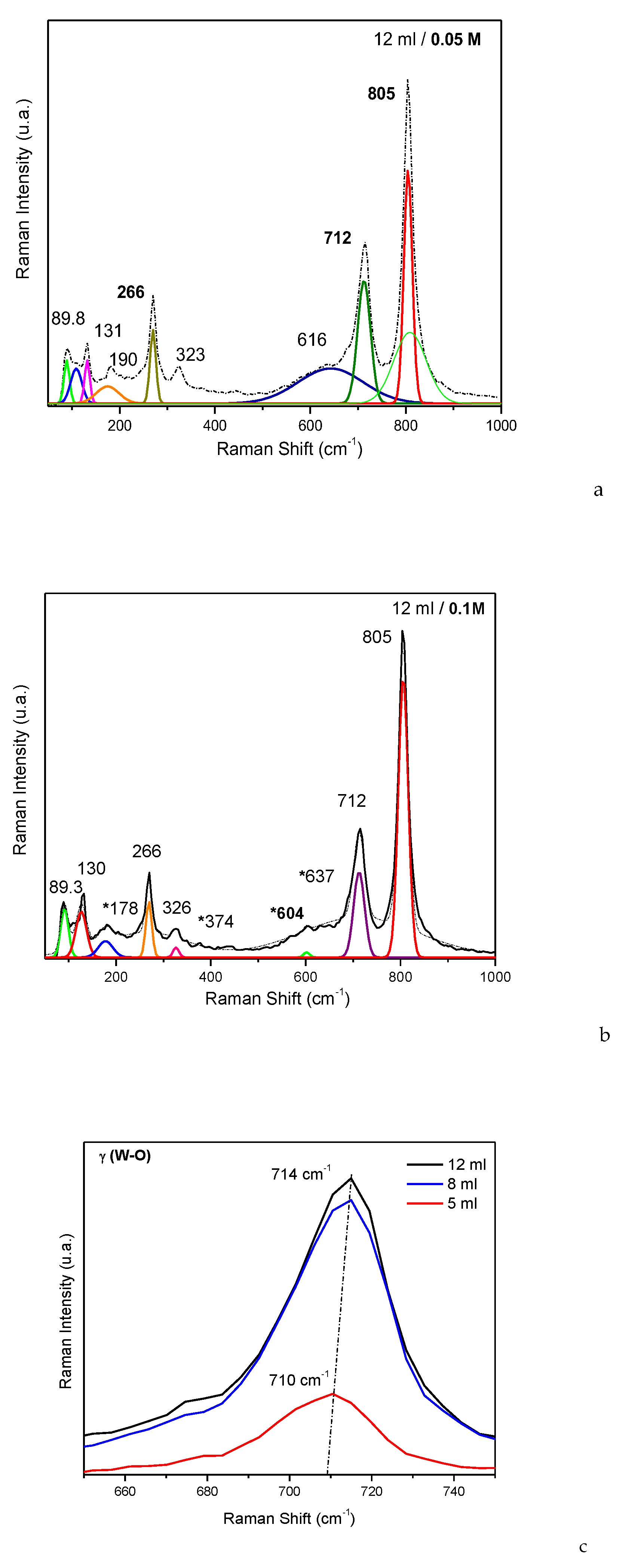
-1 region become more intense, being closely related to the increased structural order in the spray-deposited WO
3 material (
Figure 4, 12 ml volume sprayed).
The bands between 270 and 700 cm
−1 are the typical modes indicating the crystalline quality of the WO
3 films [
19].
In this case, the deposition process influenced the crystalline structure of WO
3, altering the vibration mode of certain atomic bonds in the material such as a weak δ (O-W-O), reflected through weak vibration modes in the Raman spectrum (
Figure 3), as well as the weak presence of O-lattice bonds in the spectral region around 600 cm
-1 (absence of predominant O-lattice modes at frequencies of approx. 604 and 674 cm
-1 – table 1). All these changes are induced by deviations from the ideal stoichiometry of the WO
3 composition, resulting in a variation of the atomic ratio between tungsten and oxygen
The bond at 714 cm−1, also known as the γ (W-O) band, in the Raman spectrum of WO3, indicates the vibrations of tungsten atoms bonded to oxygen atoms in the crystalline lattice. The disappearance of this band may be associated with the loss of some oxygen atom bonds in the crystal lattice.
The band at 806 cm−1 represents the Raman vibration mode of crystalline WO3 (m-phase), indicating the stretching vibrations of the bridging oxygen, νa (O−W−O).
The disappearance of symmetric νs (O−W−O) may be caused by chemical reactions leading to modification or destruction of terminal oxygen groups in the WO3 lattice. This could result from interactions with compounds during the deposition process.
Deposition of WO
3 by spray-coating induces slight shifts in the frequency of the Raman bands (
Figure 4c γ (W-O)). These shifts may be caused by changes in the local environment of the tungsten atoms or alterations in the interactions between atoms and light.
Another consequence of using the spray deposition process seems to be the decrease in FWHM Raman modes: FWHM for ν (O-W-O) mode for 5 ml decrease with ≈ 12%, the same behavior is observed for the modes γ (W-O) and νa (O-W-O) as well.
All these changes in the Raman spectrum of the spray-deposited material may be associate with the improved crystallization of the material and a reduction in the dispersion of vibration modes in the WO3 crystalline structure. The detailed Raman spectroscopy analysis of spray-deposited WO3 films provides a comprehensive understanding of structural characteristics, crystalline properties, and the influence of deposition parameters on material quality. These insights are crucial for optimizing WO3-based sensors and other applications requiring precise control over material structure and properties.


