2. Experimental Procedure
To prepare flexible buckypaper (BP), we utilized multi-walled carbon nanotubes (MWCNTs) acquired from CONJUTEK, product model CRUDE, which possess a purity greater than 95%. These MWCNTs have diameters ranging from 10 to 50 nanometers and lengths between 10 to 100 micrometers. A mass of 0.06 grams of the carbon nanotube powder was dispersed into a diluent containing Triton X-100 as a surfactant. This dispersion process involved sonication at a power of 50W for 2 hours, ensuring uniform distribution of the individual nanotubes within the liquid.
Subsequently, the dispersion was subjected to vacuum filtration. Using a vacuum pump, the liquid was passed through filter paper, resulting in the collection of BP on the paper. The resultant BP film was then carefully peeled off from the filter paper and immersed in ethanol for two hours, followed by an additional hour of immersion in deionized water. This dual soaking process was employed to eliminate any residual Triton X. Finally, the BP was air-dried in a desiccator for 24 hours to ensure complete removal of moisture.
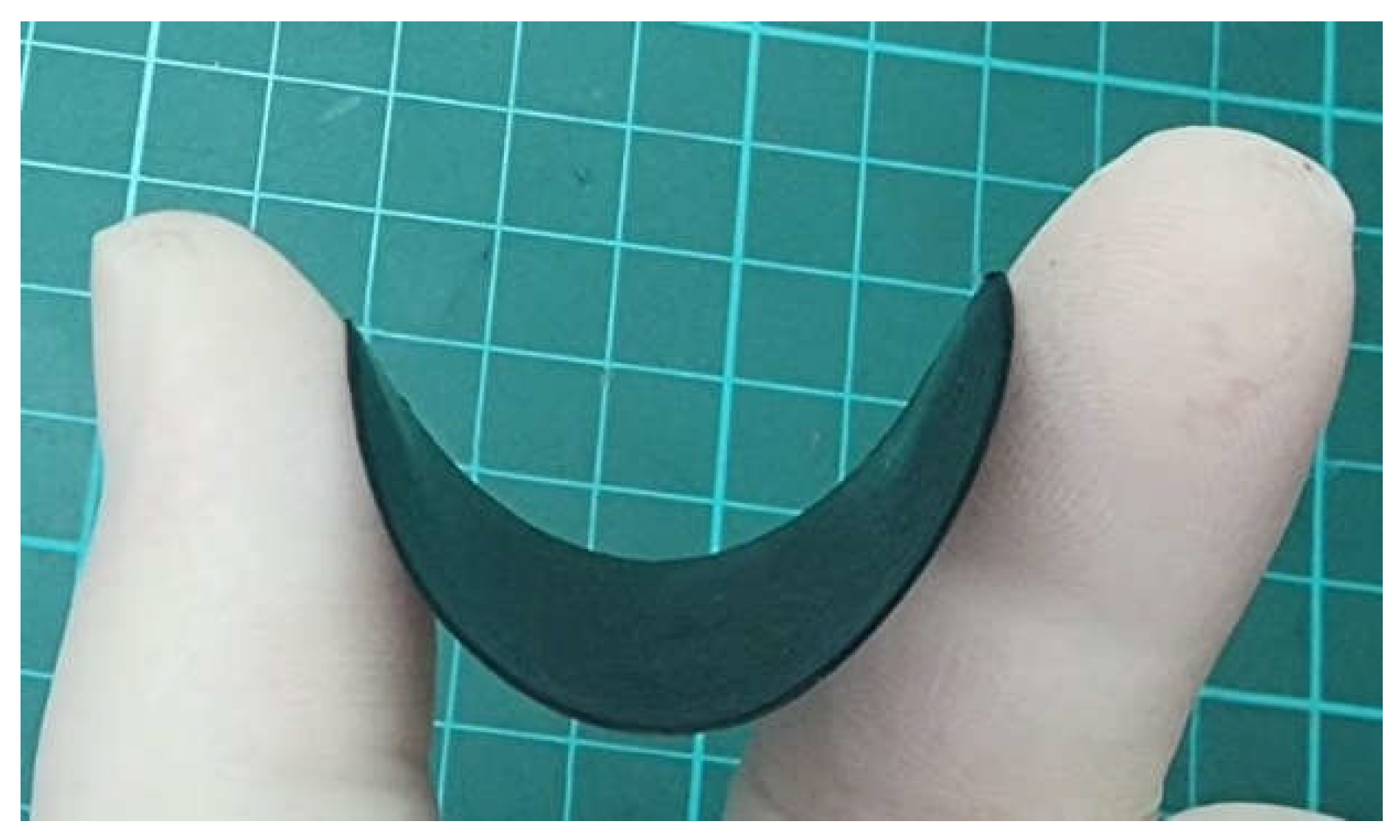
The final product was a flexible BP with a weight of 0.06 grams, a diameter of 4.5 cm, a thickness of 0.075 mm, and a porosity of 78%, as illustrated in
Figure 1. For subsequent experimentation, the BP was cut into rectangular strips measuring 2.0 cm by 0.5 cm. These strips were then subjected to various experimental conditions for plasma treatment and optoelectronic measurement.
To enhance the optoelectronic response of buckypaper (BP), we employed a gas ion plasma treatment system (Junsun Tech. CS-400, New Taipei City, Taiwan). The experimental parameters for the plasma treatment are detailed as follows: the type of gas used was varied among argon, nitrogen, and oxygen. The working gas pressure was maintained at a constant 30 mTorr, and the gas flow rate was fixed at 20 standard cubic centimeters per minute (SCCM). The plasma power was varied across different levels—5W, 10W, 20W, 30W, and 50W. Within each sample, distinct regions were demarcated and subjected to plasma modification for different durations of 1 minute, 2 minutes, 3 minutes, or 4 minutes, thereby creating gradients in carrier concentration.
For the measurement of the BP samples' optoelectronic properties, we utilized a solar simulator (A.M. 1.5G Forter Tech. LCS-100, Taichung City, Taiwan). This simulator features a standard AM 1.5G spectrum and an adjustable irradiance range of 0 to 1500 W/m². Silver paste was used to affix electrode wires onto the BP samples, which were then connected to a Keithley 2000 digital multimeter (Cleveland, OH, USA) to measure photovoltage and photocurrent.
The illumination modes were categorized into uniform full illumination and gradient illumination. Under uniform full illumination, the entire surface of the BP sample was exposed to the light source. For gradient illumination, we placed a gradient neutral density filter at the exit of the light source to achieve a gradually diminishing light intensity across the BP sample, ranging from high to low intensity. This gradient in light intensity consequently created varying carrier concentration gradients.
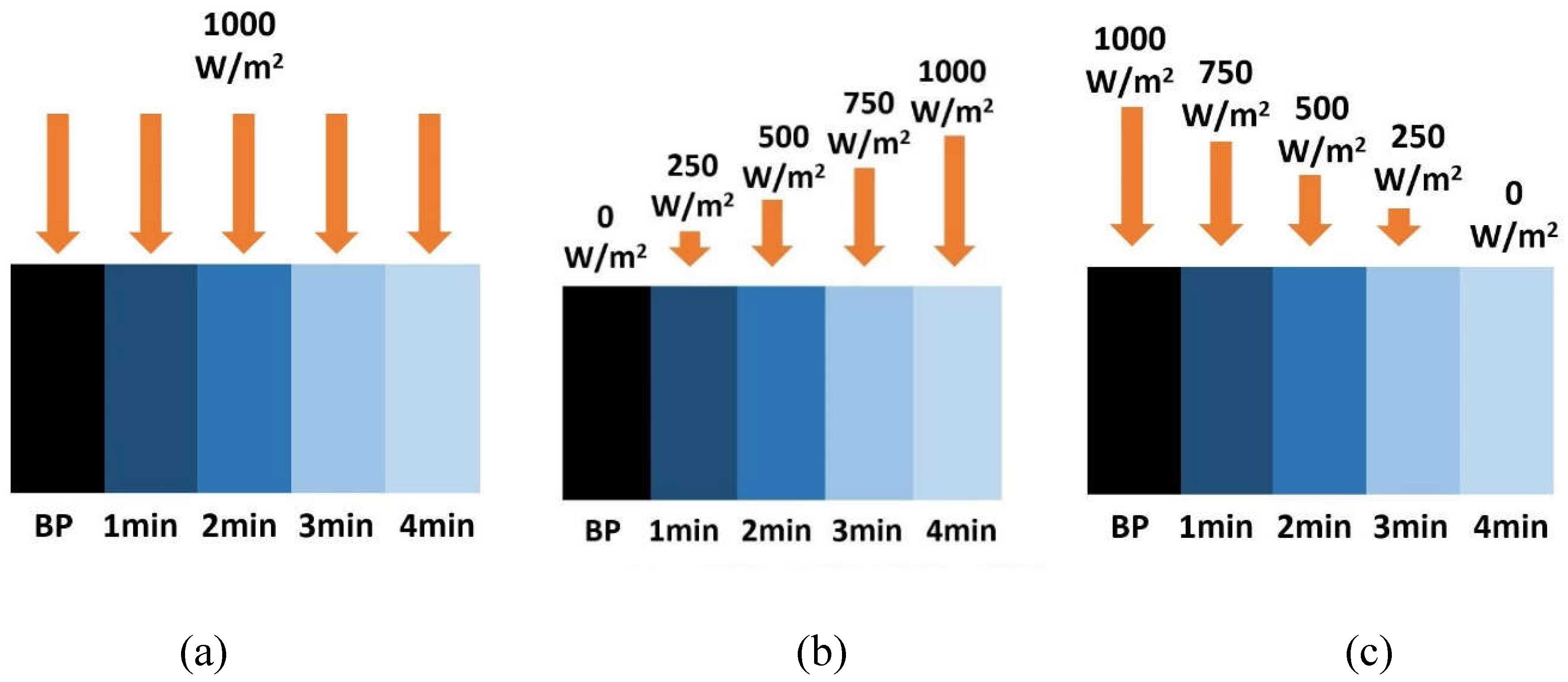
Moreover, based on the directions of the p-type carrier concentration gradients induced by both plasma modification and gradient illumination, we classified the gradient illumination modes into forward and reverse gradients. The forward gradient mode aligns the direction of the illumination gradient with the plasma gradient, while the reverse gradient mode opposes it. The schematic diagram illustrating these modes is depicted in
Figure 2.
To validate the variations in carrier concentration resulting from different plasma treatment durations or varying levels of illumination, we employed a Hall measurement system (Keithlink Tech., Taipei City, Taiwan). Utilizing the van der Pauw method, we conducted four-point probe measurements to ascertain the carrier concentration in the BP samples. Post-treatment with argon plasma at varying power levels, we observed slight modifications in the surface morphology, which were examined using a Field Emission Scanning Electron Microscope (FESEM, JEOL JSM-7000F, Tokyo, Japan).
To delve deeper into the changes in surface defects of the carbon nanotubes following plasma modification, we utilized Raman spectroscopy (Andor BWII RAMaker SR-750). The BP samples were placed on glass slides and scanned with a laser beam at an excitation wavelength of 532 nm. The Raman spectroscopic analysis was performed by measuring the intensity and wavelength of the scattered light to detect alterations in the nanotube surface.
3. Results and Discussion
To verify that the carrier concentration of untreated buckypaper (BP) changes under illumination, we manually adjusted the solar simulator to output different light intensities. The BP samples were uniformly illuminated and the carrier concentration was measured using the Hall effect method under various light intensities, specifically at 0, 250, 500, 750, 1000, and 1500 W/m². The results are presented in
Figure 3a.
Untreated BP exhibited p-type semiconductor behavior, indicating that holes are the predominant carriers. As the light intensity increased, the carrier concentration decreased from 9.22×1018 cm-3 at 0 W/m² to 0.96×1018 cm-3 at 1500 W/m². This decline is likely due to the recombination of photoinduced electron-hole pairs, which reduces the number of free carriers in the BP.
Subsequently, we introduced a gradient neutral density filter in front of the light source to produce a gradient light, aimed at enhancing the sample's photoelectric response. We then carefully moved the light intensity sensor to detect the variation in light intensity across the gradient as a function of distance, as illustrated in
Figure 3b.
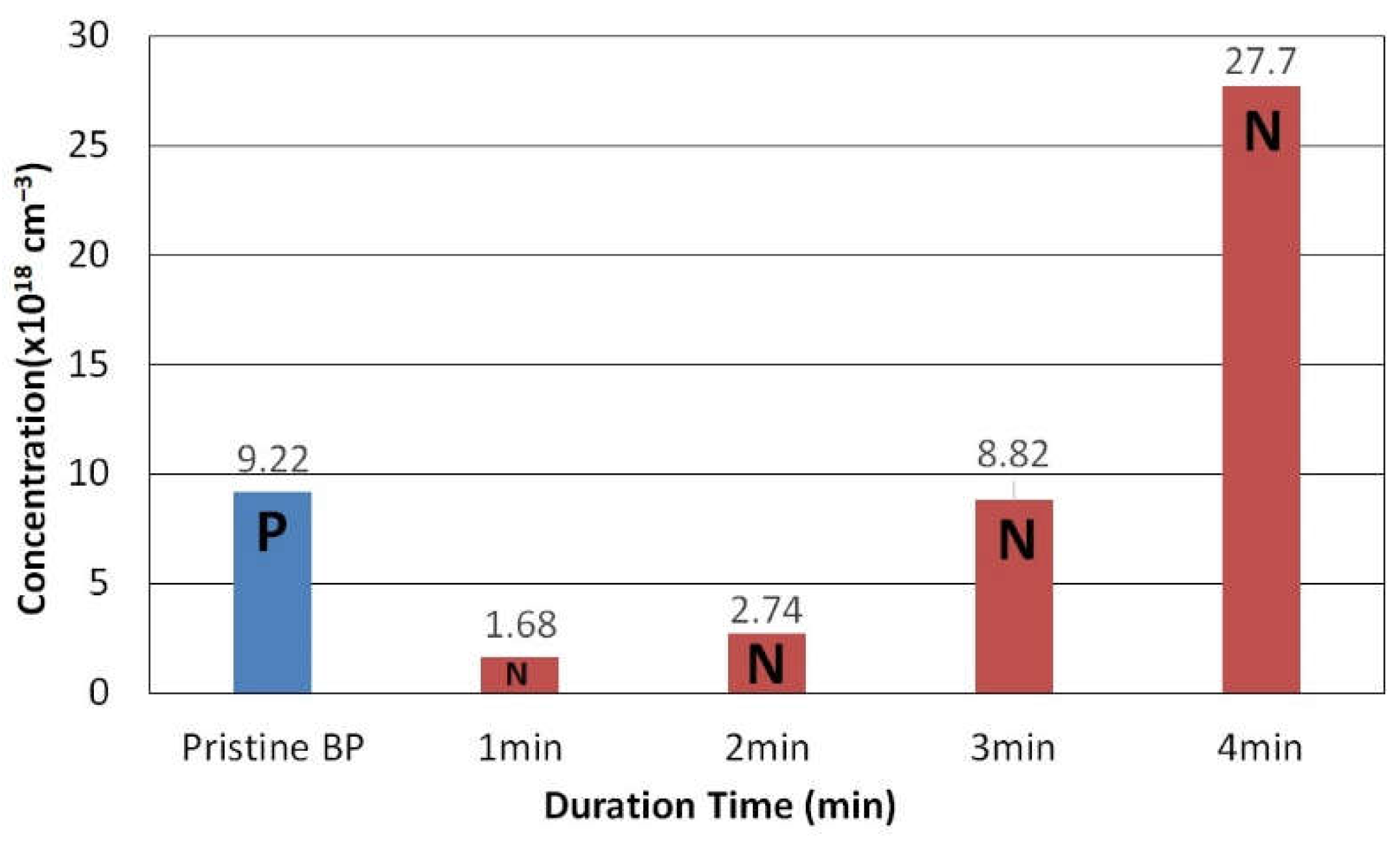
To further enhance the optoelectronic properties of buckypaper (BP), we experimented with surface modification using argon plasma at a power setting of 20W. Initially, the first sample underwent uniform plasma treatment for 1 minute, followed by measurement of its carrier concentration. We repeated these steps with additional samples, varying the plasma treatment duration to 2 minutes, 3 minutes, and 4 minutes, respectively. The carrier concentrations for each sample are illustrated in
Figure 5.
Figure 4.
Changes in carrier concentration of BP under 20W argon plasma treatment over different durations.
Figure 4.
Changes in carrier concentration of BP under 20W argon plasma treatment over different durations.
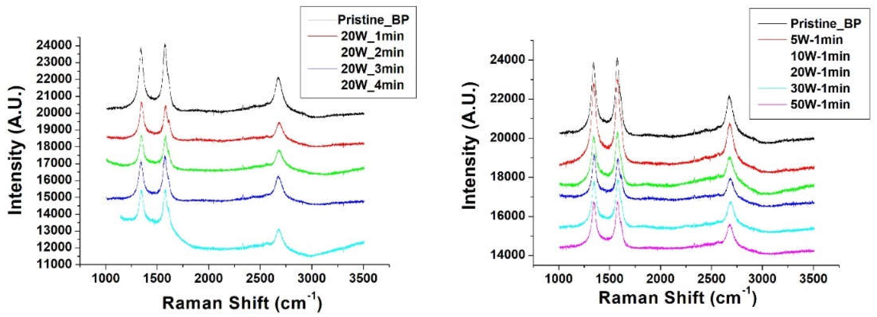
Figure 5.
Raman spectra of Buckypaper (BP) under (a) 20W argon plasma power at various treatment durations and (b) different plasma powers for a one-minute argon plasma treatment.
Figure 5.
Raman spectra of Buckypaper (BP) under (a) 20W argon plasma power at various treatment durations and (b) different plasma powers for a one-minute argon plasma treatment.
Our observations indicate that as the plasma treatment duration increased, the carrier concentration transitioned from p-type to n-type, becoming progressively more concentrated. This transition is hypothesized to result from the gradual depletion of oxygen molecules bonded to the dangling bonds on the surface of the carbon nanotubes, caused by the prolonged exposure to plasma. This phenomenon effectively alters the BP's semiconducting properties to exhibit n-type behavior [
21].
Furthermore, we varied the plasma power while maintaining a consistent treatment duration of one minute for each sample, aiming to modify the BP surface. The Raman spectra for these samples are shown in
Figure 5. The D-band, G-band, and 2D-band peaks became progressively less sharp as the power increased, indicating a broadening effect. Such broadening is typically attributed to alterations in the material's structural or chemical properties.
The D-band is commonly associated with the presence of defects within the material, while the G-band serves as an indicator of the graphitization level in carbon materials. The 2D-band, being a secondary scattering process of the G-band, can provide insights into interlayer interactions and multilayer structures.
As the plasma power increased, the introduction of additional defects or changes to the chemical structure of the carbon nanotube surface likely caused the observed broadening and decrease in peak intensity. This can be attributed to the fact that higher power plasma treatments tend to induce surface functionalization, introducing new functional groups or disrupting the existing structure of the carbon nanotubes.
In Raman spectroscopy, broadening of peaks may indicate an increase in structural disorder, which is associated with the introduction of defects. An increase in defects and irregular structures can lead to greater scattering of energy, resulting in broader peaks. Additionally, if the plasma treatment partially disrupts the graphitic structure, variations in the G-band peak shape might be observed.
Furthermore, if plasma treatment causes cross-linking between carbon nanotubes or the formation of new carbon-based structures, it could also impact the 2D-band. These structural changes would alter the electronic interactions between carbon nanotubes, thereby affecting the characteristics of the 2D-band.
In summary, the changes observed in the Raman spectra are likely due to structural defects, surface functionalization, or the disruption of the material structure induced by high-power argon plasma treatment [
22,
23]. These findings underscore the critical importance of plasma treatment conditions in modulating the properties of carbon-based materials.
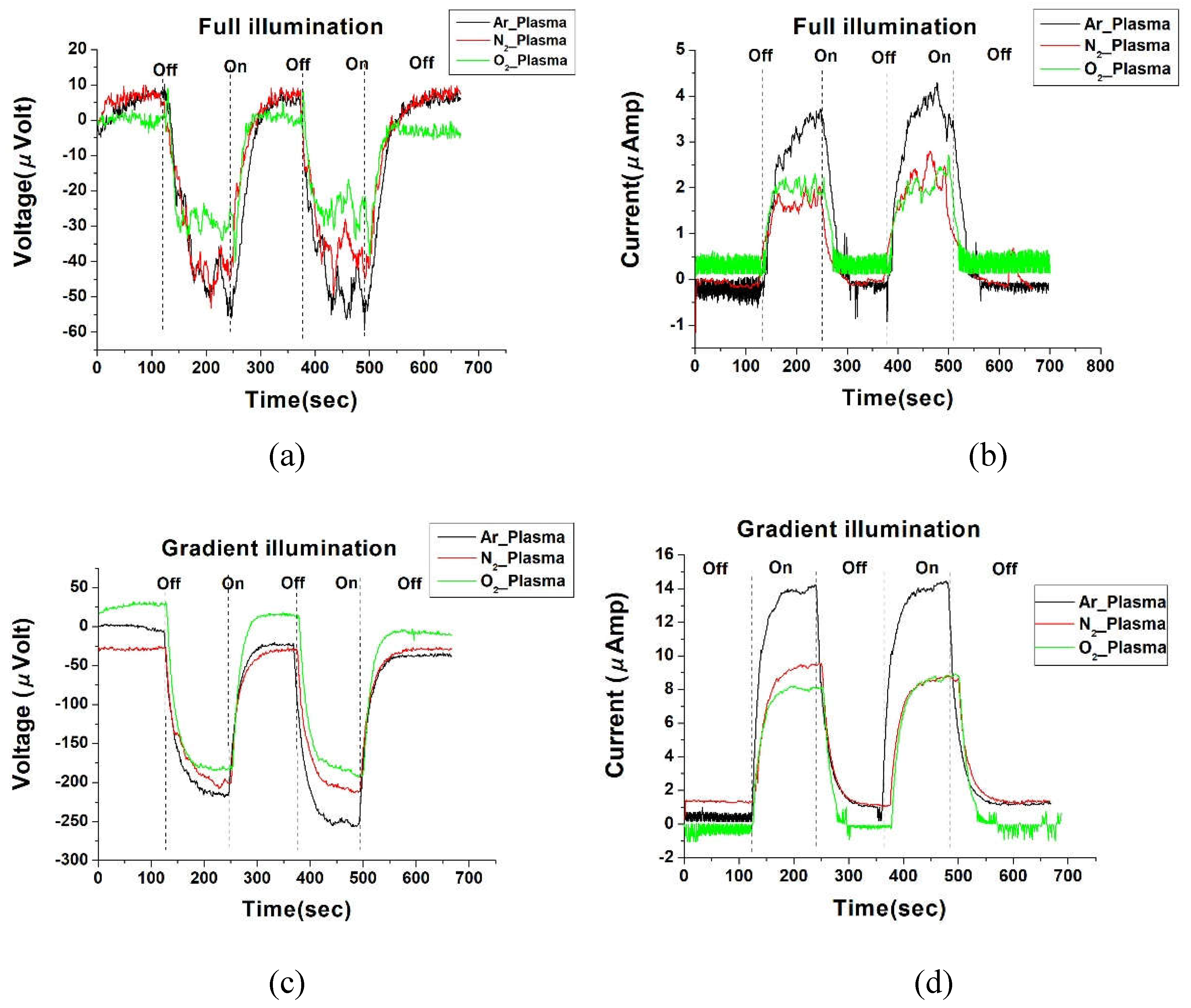
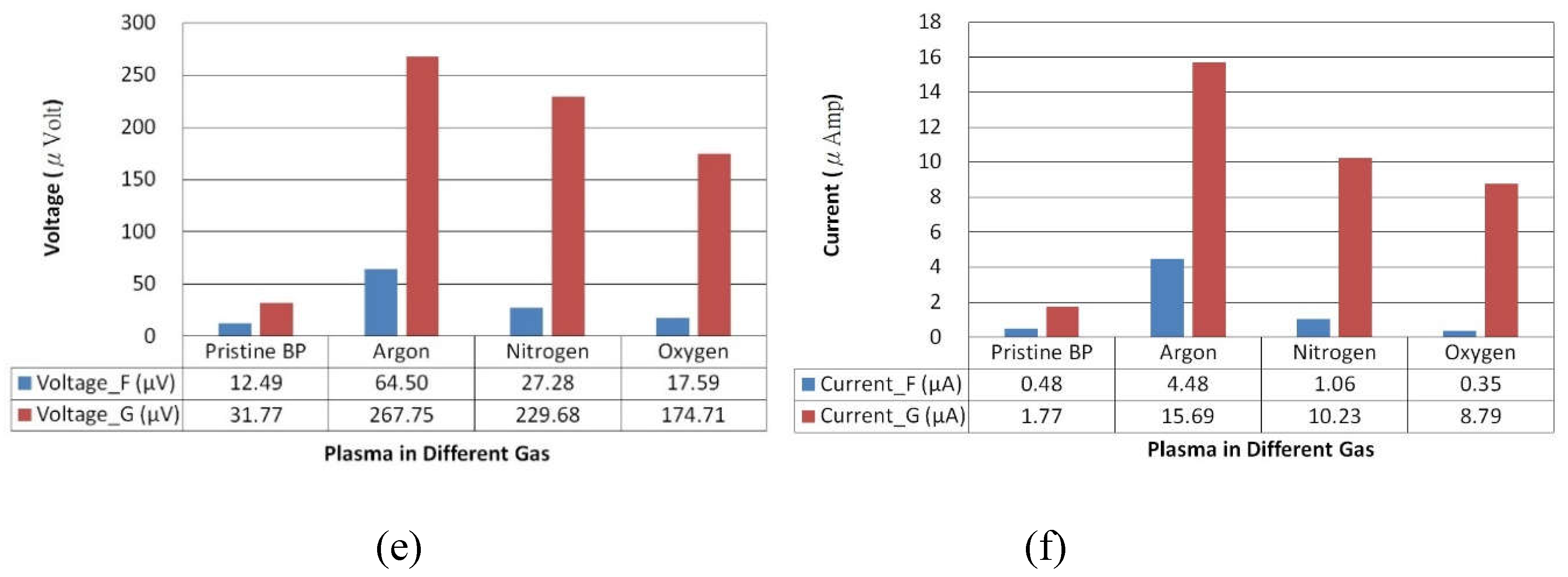
Following our preliminary findings that plasma modification can induce changes in carrier concentration, we proceeded to experiment with three different plasma gases: argon, nitrogen, and oxygen. The plasma power was maintained at a constant 20W, and the treatment duration was varied to 1 minute, 2 minutes, 3 minutes, and 4 minutes. Each segment of the BP surface underwent plasma gradient modification across consecutive spatial regions. We then measured the photovoltage and photocurrent under both uniform full illumination and forward gradient illumination conditions.
As depicted in
Figure 6a–d, it is evident that the photovoltage and photocurrent of BP samples under gradient illumination were significantly higher than those under uniform illumination. Referring to the current density equation in semiconductor materials (Equation 1), the total current density
Jp is the sum of the drift current and the diffusion current. When illuminated, numerous conductive electrons and holes are excited, and they contribute to the drift current
Jp,drift by moving under the influence of the built-in electric field. Additionally, the gradient in carrier concentration leads to an increase in
dp/
dx, the spatial derivative of the carrier concentration, which consequently enhances the diffusion current
Jp,diffusion. Therefore, the overall current increases.
In summary, the higher photoelectric response observed under gradient illumination is attributed to the creation of a significant concentration gradient within the BP, which enhances the diffusion current of carriers. Simultaneously, the mechanism underlying the photoelectric effect in BP under uniform illumination can be explained by the vibrations of the π-bonds and the mobility of π-electrons within the CNTs when exposed to light.
In this equation, Jp,drift represents the drift current, Jp,diffusion denotes the diffusion current, q is the elementary charge of the carrier, p indicates the concentration of the carriers, μp is the mobility of the carriers, E represents the electric field applied across the semiconductor material, and Dp is the diffusion coefficient for the carriers.
Additionally, under both uniform full illumination and gradient illumination conditions, the BP modified with argon (Ar) plasma exhibited the highest photovoltage, followed by the BP modified with nitrogen (N₂) plasma, while the BP modified with oxygen (O₂) plasma demonstrated the lowest photovoltage. This disparity can be attributed to the distinct effects of different plasma gases on the BP surface.
Ar plasma, being inert, primarily causes physical sputtering and etching of the BP surface. This process generates more defects and increases the surface area, thereby enhancing light absorption and carrier generation. In contrast, N₂ plasma can incorporate nitrogen atoms into the BP surface, forming C-N bonds and doping the BP with n-type impurities, which increases the electron concentration and conductivity. Meanwhile, O₂ plasma tends to oxidize the BP surface, forming C-O and C=O bonds and doping the BP with p-type impurities, which, in turn, reduce the electron concentration and conductivity.
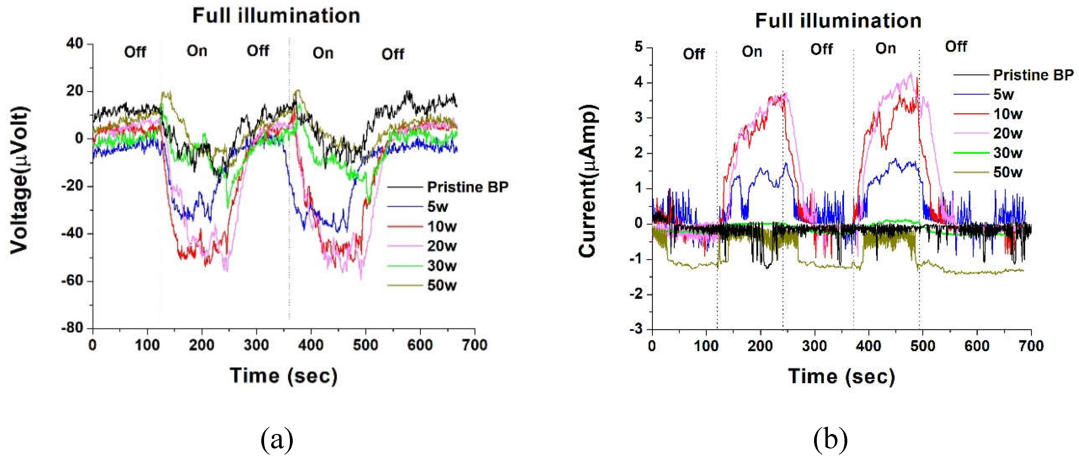
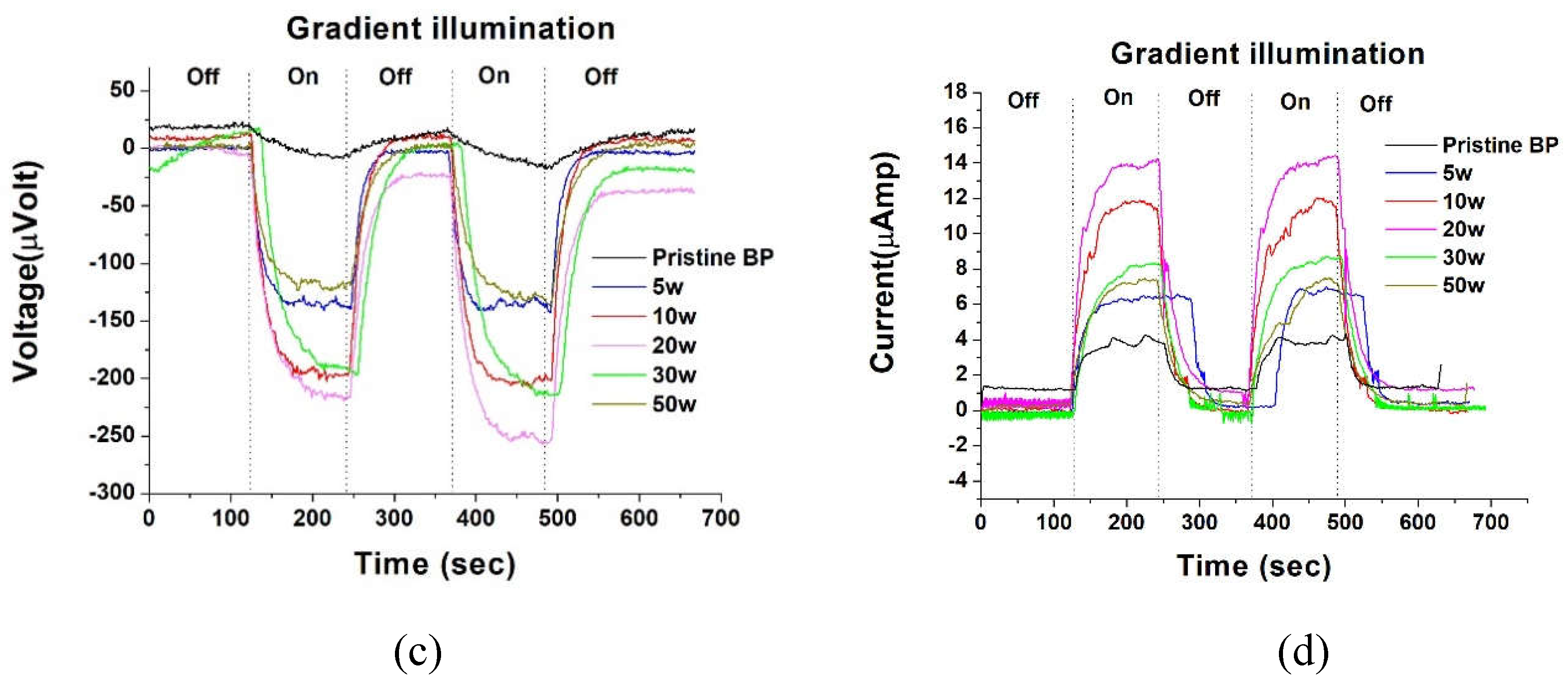
Therefore, Ar plasma modification more effectively enhances the optoelectronic properties of BP compared to N₂ and O₂ plasma modifications. Based on these findings, Ar plasma was chosen as the optimal gas for BP modification. We subsequently employed different power settings—5W, 10W, 20W, 30W, and 50W—with a treatment duration of one minute to modify the BP. The photovoltage and photocurrent responses under both uniform illumination and gradient illumination for these different power settings are depicted in
Figure 7.
We observed that BP modified with a plasma power of 20W exhibited the highest photovoltage and photocurrent under both uniform full illumination and gradient illumination modes. This was followed by BP modified with 30W plasma power, while BP modified with 50W plasma power showed the lowest photovoltage and photocurrent. This phenomenon can be explained by the balance between plasma etching and plasma damage effects.
Plasma etching tends to create more defects and increase the surface area of BP, which enhances light absorption and carrier generation. On the other hand, plasma damage can break C-C bonds and reduce the π-electron density in BP, thereby diminishing light absorption and carrier generation. As plasma power increases, the plasma etching effect becomes more pronounced, but so does the plasma damage effect. Therefore, an optimal plasma power exists that maximizes the plasma etching effects while minimizing plasma damage effects to achieve the best optoelectronic performance of BP. In this study, the optimal plasma power was found to be 20W.
To further examine the damage induced by plasma bombardment on the BP surface, we utilized a Scanning Electron Microscope (SEM) to assess the impact of plasma power on BP’s surface morphology. SEM images of BP treated with 20W and 50W Ar plasma are shown in
Figure 8.
From
Figure 8, it is evident that a plasma power of 50W inflicted severe damage on the BP surface, leading to the fragmentation and localized collapse of carbon nanotubes, which subsequently fused together. This observation substantiates the plasma damage effect and elucidates why BP modified with 50W plasma power exhibited poor optoelectronic performance. Conversely, a plasma power of 20W did not cause significant damage to the BP surface; instead, it created more defects and increased surface roughness. This supports the plasma etching effect and explains the enhanced optoelectronic performance of BP modified with 20W plasma power.
Finally, using the experimental setup depicted in
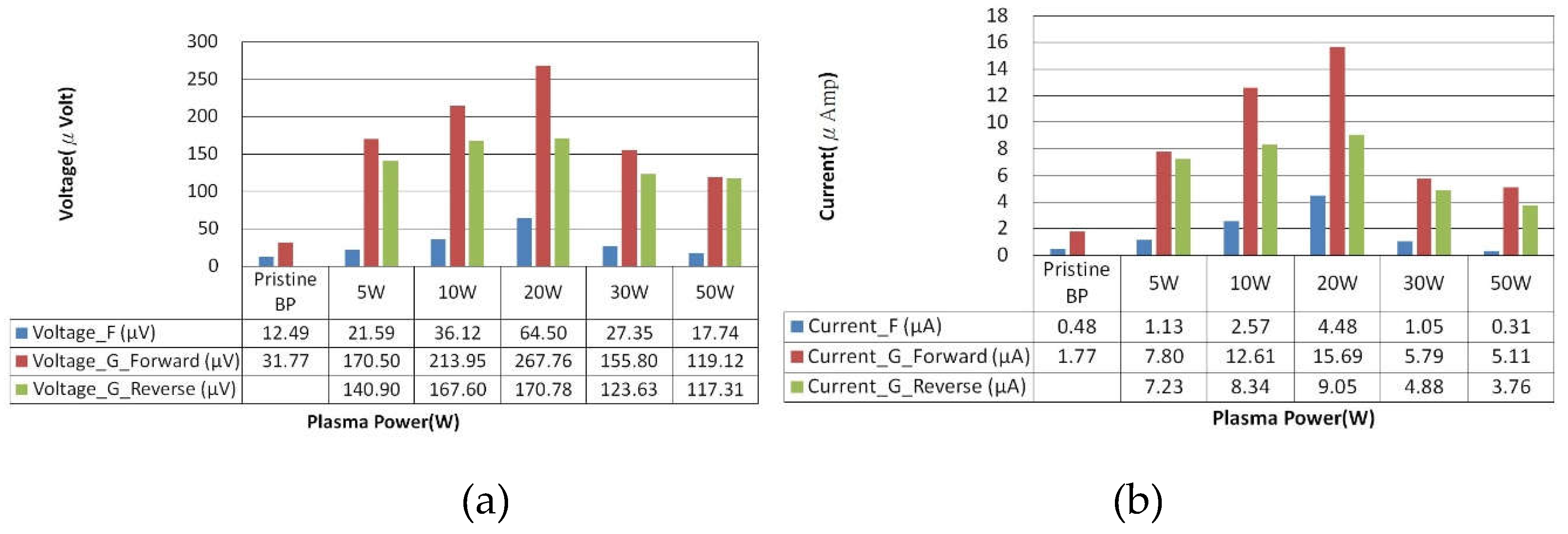
Figure 3, we applied a plasma power of 5W to different spatial regions of a single BP sample. Each region was treated for varying durations of 1 minute, 2 minutes, 3 minutes, or 4 minutes to induce carrier concentration gradients. Following the same experimental procedure, we repeated this with plasma powers of 10W, 20W, 30W, and 50W, each applied to different regions for different durations. These gradient-modified samples were then subjected to measurements of photovoltage under uniform illumination (Voltage_F), photovoltage under forward gradient illumination where the light gradient aligns with the plasma treatment gradient (Voltage_G_Forward), and photovoltage under reverse gradient illumination where the light gradient opposes the plasma treatment gradient (Voltage_G_Reverse).
From
Figure 9, we can observe the experimental setup as depicted in
Figure 2b. Assuming the positive direction is defined as rightward, the light intensity increases gradually from left to right. According to the p-type carrier concentration distribution shown in
Figure 3a, the concentration decreases to the right, indicating
Additionally, the plasma gradient time increases from left to right. Based on the n-type carrier concentration distribution illustrated in
Figure 4, the concentration increases to the right, resulting in
, which equivalently means
. When the illumination gradient aligns with the plasma gradient, the diffusion current and drift current can sum up, leading to higher photovoltage and photocurrent. Consequently, the photovoltage and photocurrent are higher when the gradients of illumination and plasma are in the same direction compared to when they are in opposite directions.
Comparatively, under uniform illumination, the intrinsic BP produced a photovoltage of 12.49 microVolts. After being modified by 20W plasma under uniform illumination, the photovoltage increased to 64.50 microVolts. Furthermore, with the addition of plasma gradient modification and gradient illumination, the photovoltage reached 267.76 microVolts, which represents a 21.44 times increase. Similarly, the photocurrent rose from 0.48 microAmps to 15.69 microAmps, achieving a 32.69 times enhancement.
