1. Introduction
Nowadays, equipment designed for military applications, such as communications or electronic warfare (EW), is experiencing a significant increase in relevance, largely due to the various conflicts that have arisen on the global stage [
1,
2]. Multifunctional RF systems (MFRF) that integrate multiple RF functions such as radar, electronic warfare (EW) or communications (COMMs) in a single system are of particular interest today [
3,
4,
5,
6]. To achieve this capability, active electronically scanned array (AESA) systems are an essential technology. In this regard, the CROWN Project represents an initial stage in the development of a fully European AESA with combined radar, COMMs, and EW functions. The main objective of the CROWN Project is to demonstrate the integrated and coordinated operation of the different functions (Radar, EW, COMMs) in a digital RF AESA system[
7,
8,
9]. The project is being carried out by the main representatives of the European defense industry. In total, 11 entities from 7 European countries.
AESA systems are based on an array of antennas with a transmission (Tx) and reception (Rx) module connected to each of the radiating elements. These Tx/Rx modules consist on a high-power amplifier (HPA) in Tx mode and a low-noise amplifier (LNA) in Rx mode. To switch between Tx and Rx modes single-pole double-throw (SPDT) switches are included to provide this capability. Additionally, beamforming elements are placed in each channel, such as a phase shifter or a real-time delay circuit (TTD), to generate the required phase shift enabling electronic scanning capabilities. The HPA, LNA, and beamforming elements are typically packaged in monolithic microwave integrated circuit (MMIC) modules that are placed into the array structure to be as close as possible to the radiating elements, minimizing system losses.
In the space and military electronics industry, the use of Gallium Arsenide (GaAs) technology for implementing various subsystems has become well-established, largely due to the following characteristics: low noise level, high operating frequency, moderate power level, and excellent immunity to radiation interference [
10,
11,
12,
13,
14]. However, in the defense and satellite domains, even more demanding requirements needed, requiring receivers with superior robustness and the ability to handle even higher power levels [
15,
16,
17,
18]. The robustness of these devices must be optimal to ensure their operation in any condition, whether in terrestrial military environments or the vacuum in the space. This mplies that designed receivers [
20,
21] that use robust circuits and redundant systems in the various subsystems, such as the low-noise amplifiers (LNA), high-power amplifiers (HPA), driver amplifier (DA), mixers, combiners, and even filters. Implementing these redundancies and employing durable materials are crucial for reducing the risks associated with potential failures and ensuring the continuity of operations in hostile environments.
In this context, GaN technology emerges as an extremely promising option for developing robust subsystems and circuits[
22,
23]. Besides its capability to handle high power levels, GaN exhibits a low noise factor, making it a strategic choice for applications in adverse environments such as space and military industries [
16,
17,
24]. The use of gallium nitride (GaN) technology for designing MMICs has grown over the past decade due to its specific properties that make it particularly suitable for designing active RF components [
17,
24,
25,
26,
27,
28,
29]. In comparison to other technologies, like gallium asenide (GaAs) [
30,
31,
32,
33,
34,
35,
36], Gallium nitride (GaN), as one of the wide bandgap semiconductors, presents a high electric breakdown field and a high electron saturation velocity. Compared to gallium arsenide (GaAs) and silicon (CMOS or LDMOS) power amplifiers [
11,
37,
38,
39,
40,
41], GaN power amplifiers exhibit higher output power, greater efficiency, wider bandwidth, and better thermal characteristics. Therefore, GaN technology is a strong candidate for high-performance high-power amplifiers [
42,
43,
44,
45,
46,
47]. Among these characteristics, the most important are the wide bandgap and the high breakdown voltage, which allow MMICs to operate at higher voltages, higher saturation speed, and higher power density compared to conventional GaAs circuits. Additionally, GaN offers excellent thermal conductivity, especially when placed on high-conductivity substrates like silicon carbide (SiC).
Consequently, GaN technology is positioned as a key element for advancement and innovation in these fields, promising to drive the continuous evolution of technological capabilities in space exploration and national defense. In this article, is presented the design of an HPA using 250 nm GaN pHEMT technology from LEONARDO semiconductor’s standard GaN pseudomorphic high electron mobility transistor MMIC technology on a substrate thickness of only 100 µm for MFRF systems. Both the output power and the Power Added Efficiency (PAE) are maximized in the frequency band from 2 to 10 GHz at a nominal supply voltage of 28 V.
Additionally, parameters such as bandwidth, large-signal gain, and the compression point not only contributes to the academic understanding of circuit design also has practical implications for real-world applications. This study offers valuable insights for optimizing future circuit designs and improving overall system efficiency. Moreover, the comprehensive nature of the analysis, which encompasses both design considerations and experimental validation, underscores the rigor and validity of the data presented. Through systematic evaluation, this work establishes a solid foundation for future advancements in MMIC technology and contributes to the evolution of high-frequency electronic systems.
In conclusion, this research represents a significant advancement in the field of circuit design and evaluation, demonstrating the successful integration of advanced semiconductor technology with rigorous experimental validation. This work offers valuable contributions to both academic research and practical applications in the realm of high-frequency electronics. Also accompanied by a comparative analysis between simulations and measurements. This work demostrates the successful implementation and evaluation of the circuit, and the viability and effectiveness of the chosen approach. Moreover, the utilization of advanced semiconductor technology from LEONARDO highlights the commitment to leveraging cutting-edge materials and methods in the pursuit of high-performance electronic solutions.
The article is structured as follows. First, the GaN HEMT technology used and its transistor characteristics will be described. Followed by the design and analysis of the proposed HPA. The measured performance of the fabricated amplifier will be provided and discussed before the conclusion.
After the introduction, the main design requirements and objectives are presented in
Section 2 under the heading "Issues of Broadband HPA Design." This section includes a series of subsections detailing the initial specifications imposed by
INDRA company, the description of the GaN technology used in this project for the design and integration of the HPA MMIC, and the selection of the architecture chosen for the design.
In
Section 3, a brief description of the HPA is provided, identifying the main critical aspects.
Section 4 presents the measurement setup. For this purpose, the amplifier was assembled in a test bench. The design has been measured “on wafer” and “on jig” and compared with the simulation of the completed design.
Finally,
Section 5 and 6 conclude with a comparison and discussion of the obtained design characteristics and their comparison with the state of the art and other consulted references. The article ends with conclusions about the work carried out and the constructed MMIC.
2. Issues of Broadband HPA Design
2.1. Specifications of Design
Before undertaking any design, the initial specifications for the proposed design must first be presented.
Table 1 shows the initial specifications imposed by
INDRA company for the design presented in this article.
These specifications (
Table 1), as well as the GN25 process from the LEONARDO GaN foundry, will greatly influence the presented solution, as will be demonstrated in the following sections. As we can see, the initial specifications imposed by
INDRA company are stringent and pose a significant technological challenge that will prove difficult to meet.
Another important aspect to highlight is the large-signal gain specifications, along with the required input power and the number of stages of the HPA, are determined by the application for which the HPA MMIC will be used. The size of the MMIC HPAs is largely dictated by the size of the output stage (output power) and the number of stages required to achieve the desired large-signal gain. Therefore, compliance with the size specification imposed by the
INDRA company will be conditioned by the desired power level and large-signal gain.
2.2. Process GN25
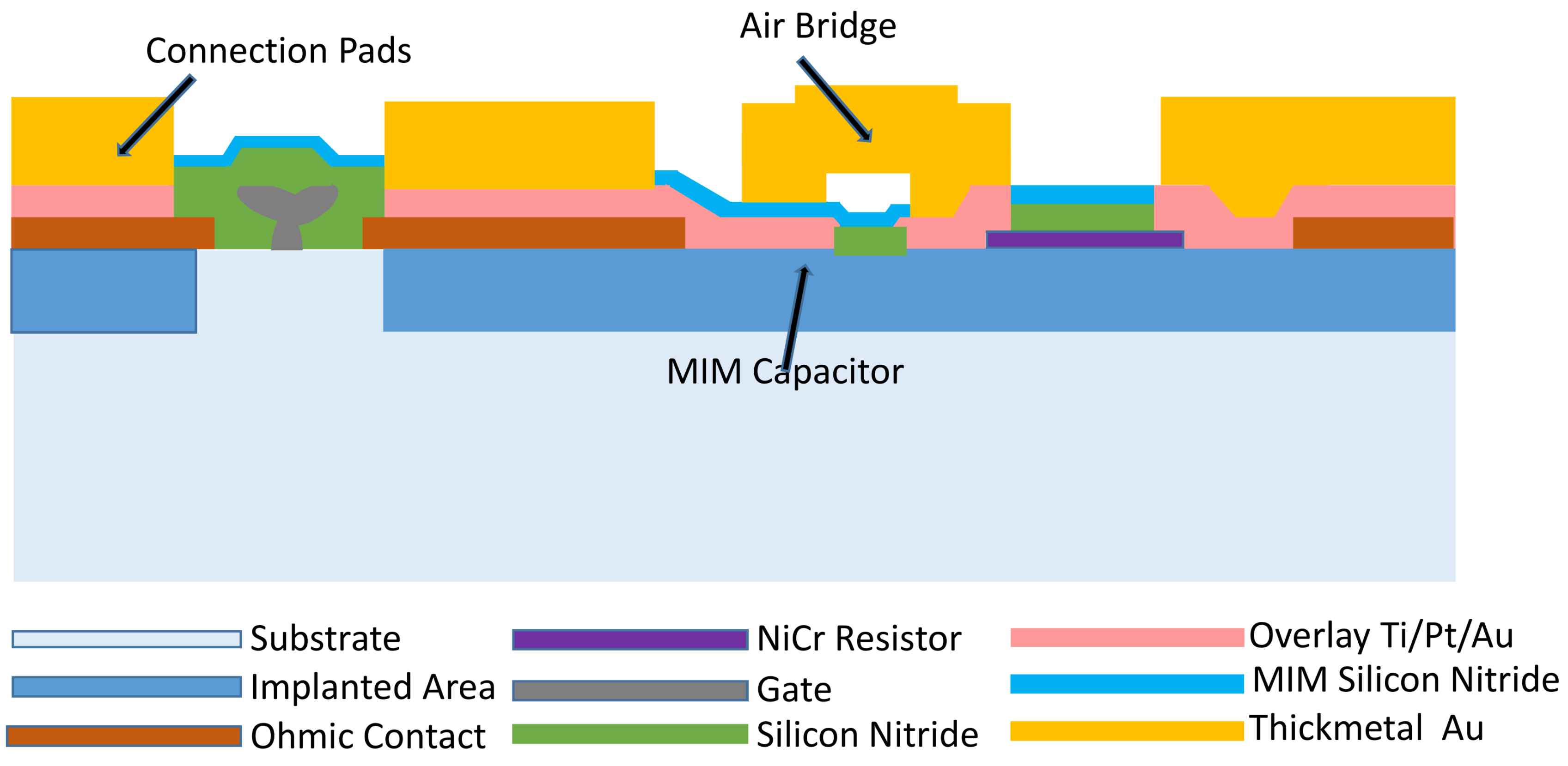
The GN25 process is an 0.25
m gate length and slanted gate-foot profile in AlGaN/GaN with high electron mobility transistors (HEMT technology) from LEONARDO. The first version of HEMT technology dates back to 2022. In
Figure 1, a brief schematic of the GN25 process is shown.
The LEONARDO process provides a current gain cut-off frequency
> 22 GHz, and a maximum oscillation frequency
> 44 GHz. The wafer is thinned in 100
m. This process is suitable for applications up to 20 GHz with cutting-edge figure of merits in terms of power, gain, and reliability.
Table 2 shows the most important characteristics of the MMIC process, provided by the foundry.
Moreover, the MMIC process includes precision Tantalum Nitride resistors (TaN resistors), high values titanium tungstosilicate resistors (TiWSi resistors), Metal-Insulator-Metal capacitors (MIM capacitors), inductors, air-bridges, via-holes through the substrate, CAD models for passive elements and microstrip transmission lines.
It is important to indicate that the GN25 is a process developed for the fabrication of HPAs.
Table 3 shows the measured characteristics on wafer at large signal working at room temperature (To=25°C) in continuous wave (CW) for a transistor of size 10x100
m.
The authors of this article used the
LEONARDO’s GN25 process because this technology targets the design of monolithic integrated robust high power MMICs besides and by
INDRA company specification.
2.3. Selection of Architecture of the HPA
Based on the data provided by LEONARDO in the preliminary analysis
Section 2.1, the design specifications
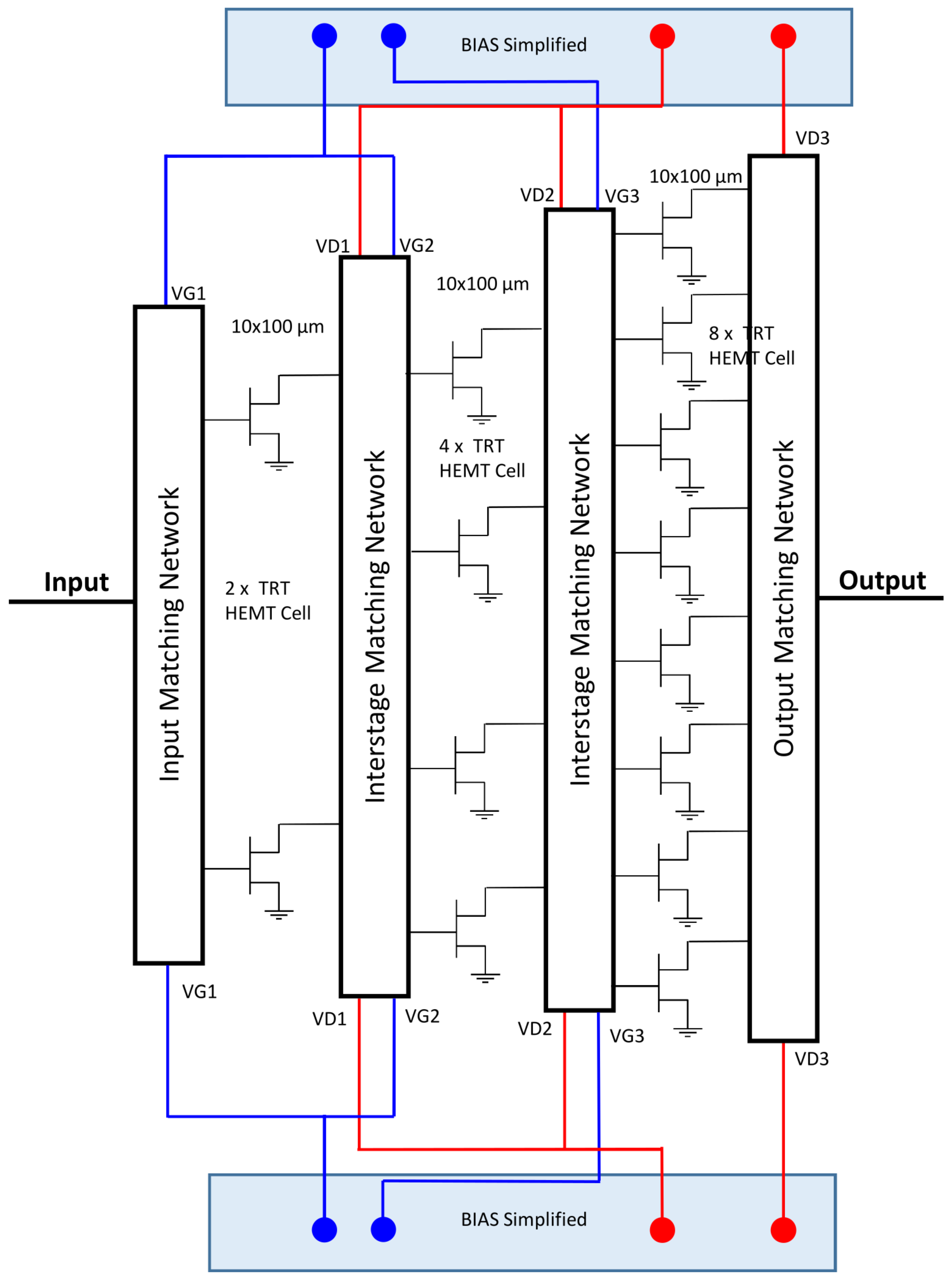
Section 2.2, and taking into account the thermal, electrical, and physical constraints of the technology, a three-stage corporate architecture (2+4+8 transistors) is chosen for the MMIC HPA. Its block diagram is shown in
Figure 2, where all transistors in the selected architecture have a size of 10x100
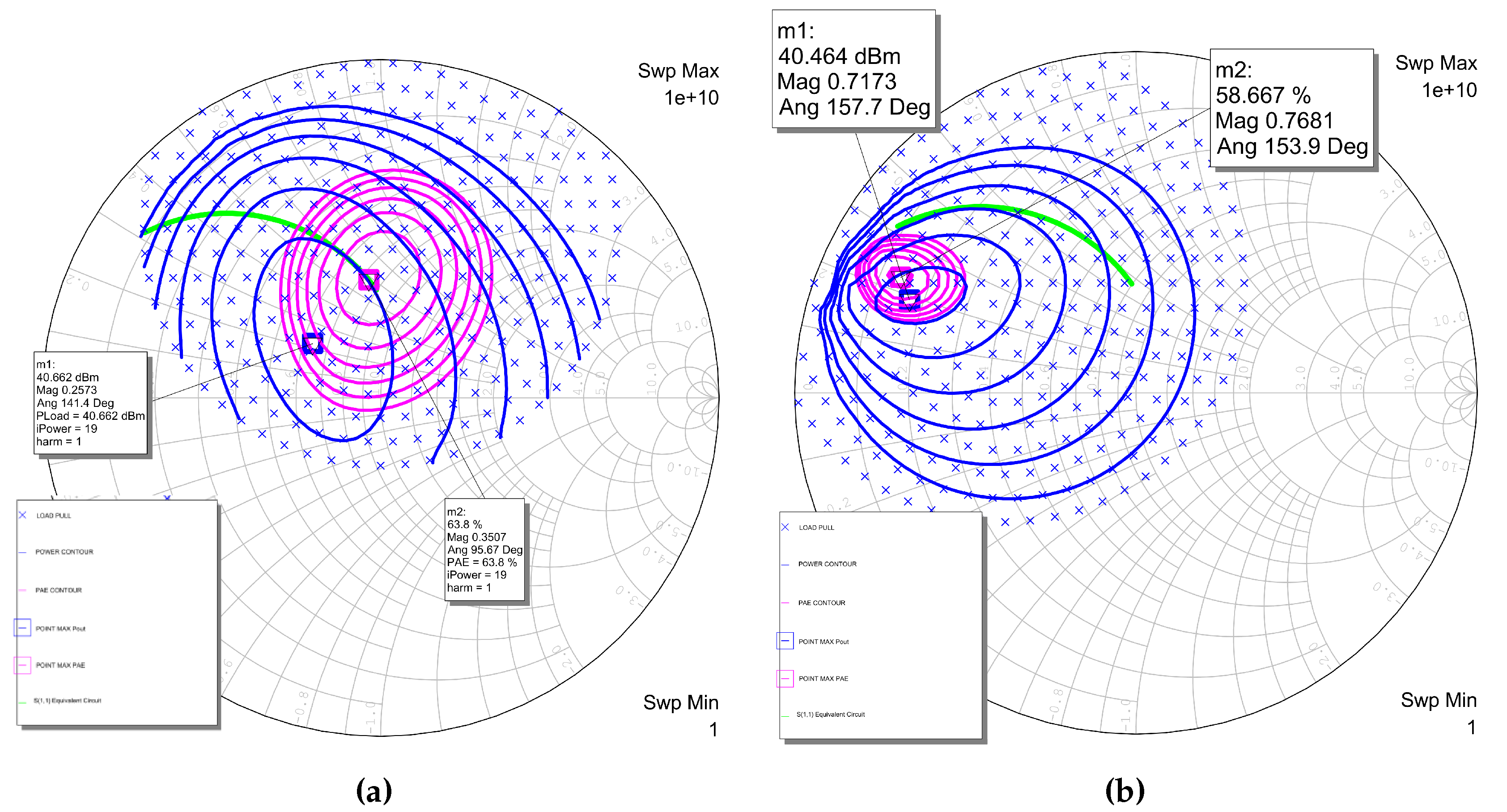
m. This transistor choice is due to prior characterization work through Load-Pull simulations using the AWR software version 17 [
48]. Although LEONARDO also provides the PDK for the
ADS[
49] software, this variant presents issues when carrying out the final design.
Figure 3 shows the Load-Pull analysis for the 10x100
m transistor at frequencies of 2 GHz and 10 GHz, respectively. The figure additionally represents an RC equivalent circuit used to model the output impedance of the transistor.
Once the transistor is selected, the architecture shown in
Figure 2 consists of two transistors and four transistors of size 10x100
m for the input and intermediate stages. The final stage is based on the combination of eight 10x100
m transistors in parallel, each providing approximately 33 dBm of output power. This size has been determined taking into account the power density of Leonardo’s technology to achieve more than 20 W (43 dBm) at the device’s output.
To simplify the interconnections of the MMIC, the same bias was adopted for all stages, i.e., VDD = 30 V and VGG = −3.0 V. This corresponds to a quiescent current of 62.5 mA for each device, resulting in currents of 500 mA, 250 mA, and 125 mA in the final, intermediate, and input stages of the HPA, respectively. This choice is the result of a compromise between electrical performance and the capabilities provided by the LEONARDO PDK.
3. Hpa Networks Strategy, Simulations and Design
Once the architecture was established and the transistors were selected, the next step was to concisely describe the strategy followed in the design. The authors have described the steps taken and the strategy employed in the design of the HPA MMICs in greater detail in the article [
50].
The optimal operating class depends on the application area. This high-power amplifier discussed in this work is designed for applications in EW. Therefore, the most important requirements are both output power and added power efficiency (PAE) simultaneously. Hence, class-AB is the best choice to achieve these requirements. In this design, all stages have been biased in class-AB to ensure PAE performance. This biasing point which guarantees accurate nonlinear simulation.
As described in [
50], the synthesis of input and output impedances to maximize output power and PAE for each stage, along with the power distribution and combining networks, constitute the essential aspects of simulating the HPA MMIC design [
51,
52]. In a design for wide bandwidth, harmonics are of little importance and are matched to 50 ohms. The design of impedance matching networks and power distribution/combining networks was initially approached using the equivalent circuit extracted from the Load-Pull, as described in [
50].
In
Figure 4, the test bench in
AWR is shown for calculating all the required specifications mentioned in
Section 2.1.
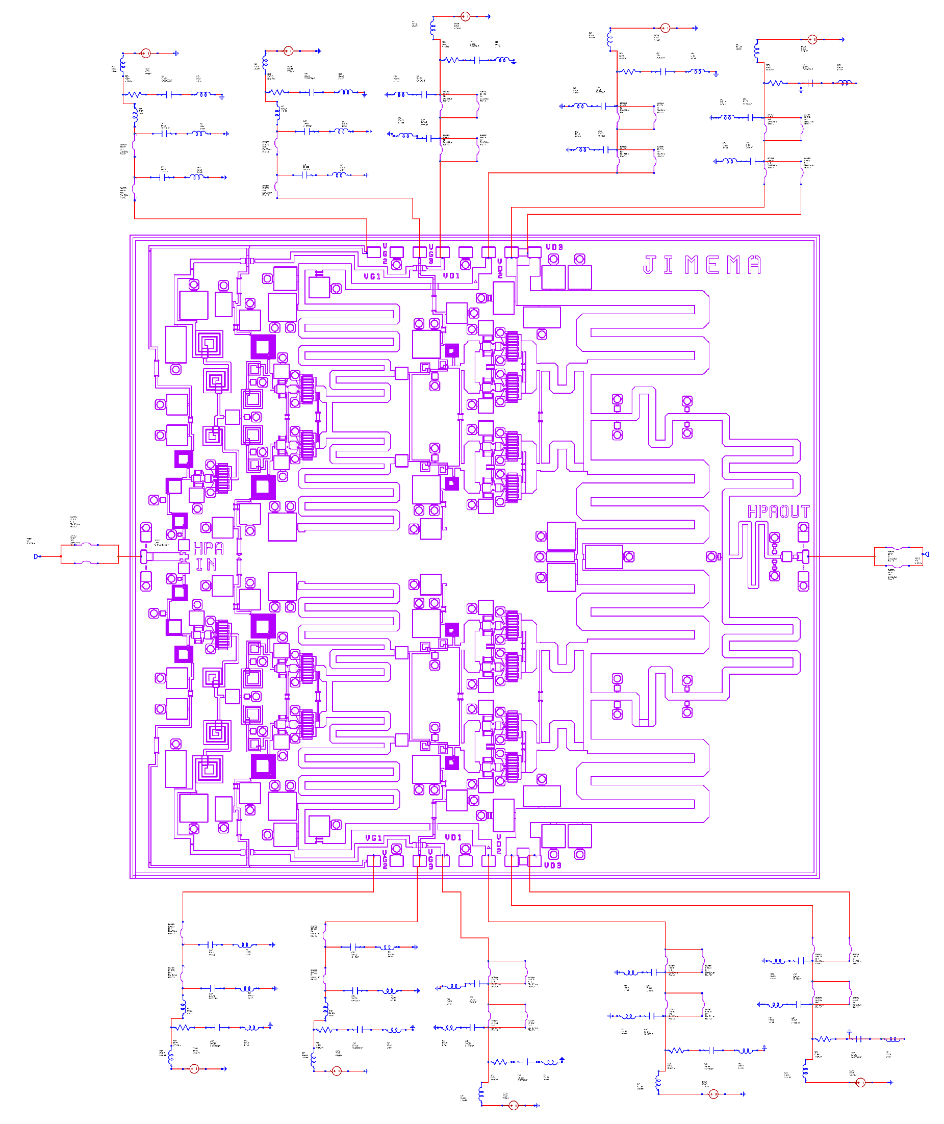
In the final design, the transmission lines and connection lines modeled by the Leonardo PDK with real lines are simulated by the EM simulator. This is due to the proximity and bandwidth of the specified frequencies. Therefore electromagnetic simulation is employed with the assistance of AXIEM.of
AWR. In
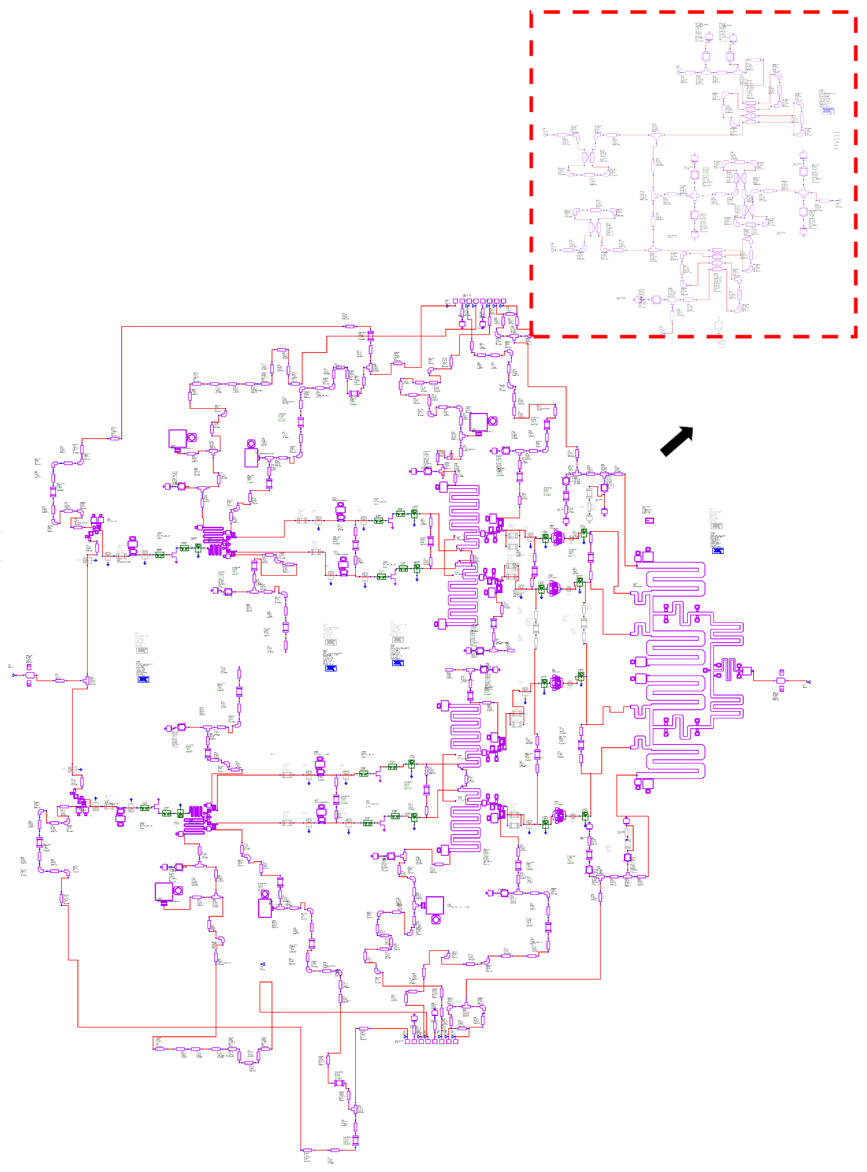
Figure 5, a schematic of the designed HPA is shown, illustrating the complexity of the design and the various networks comprising it
The AXIEM electromagnetic tool from
AWR software allowed us to assess the effect that lines and passive elements have on the final behavior of the designed broadband HPA. In the simulations carried out, the circuit model for the lines and passive elements, provided by the LEONARDO foundry, and the electromagnetic model that the ADS software allows modeling were studied.
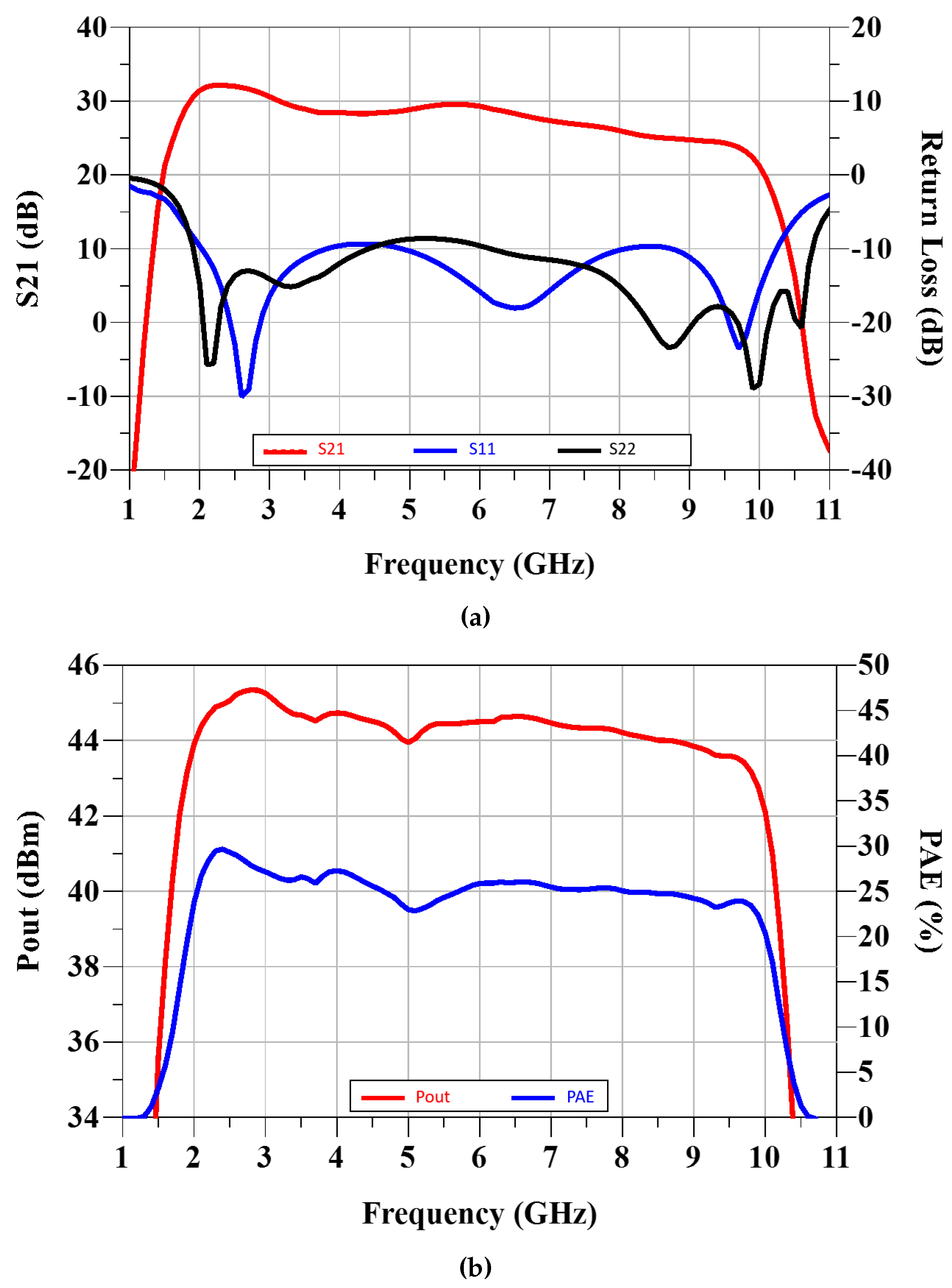
Figure 6 and
Figure 6 display the results of the small-signal and large-signal parameters of the final designed MMIC. As we can be observed, these simulations enable the prediction of meeting the initial requirements.
After this performance verification, the HPA MMIC is fabricated at the LEONARDO Foundry.
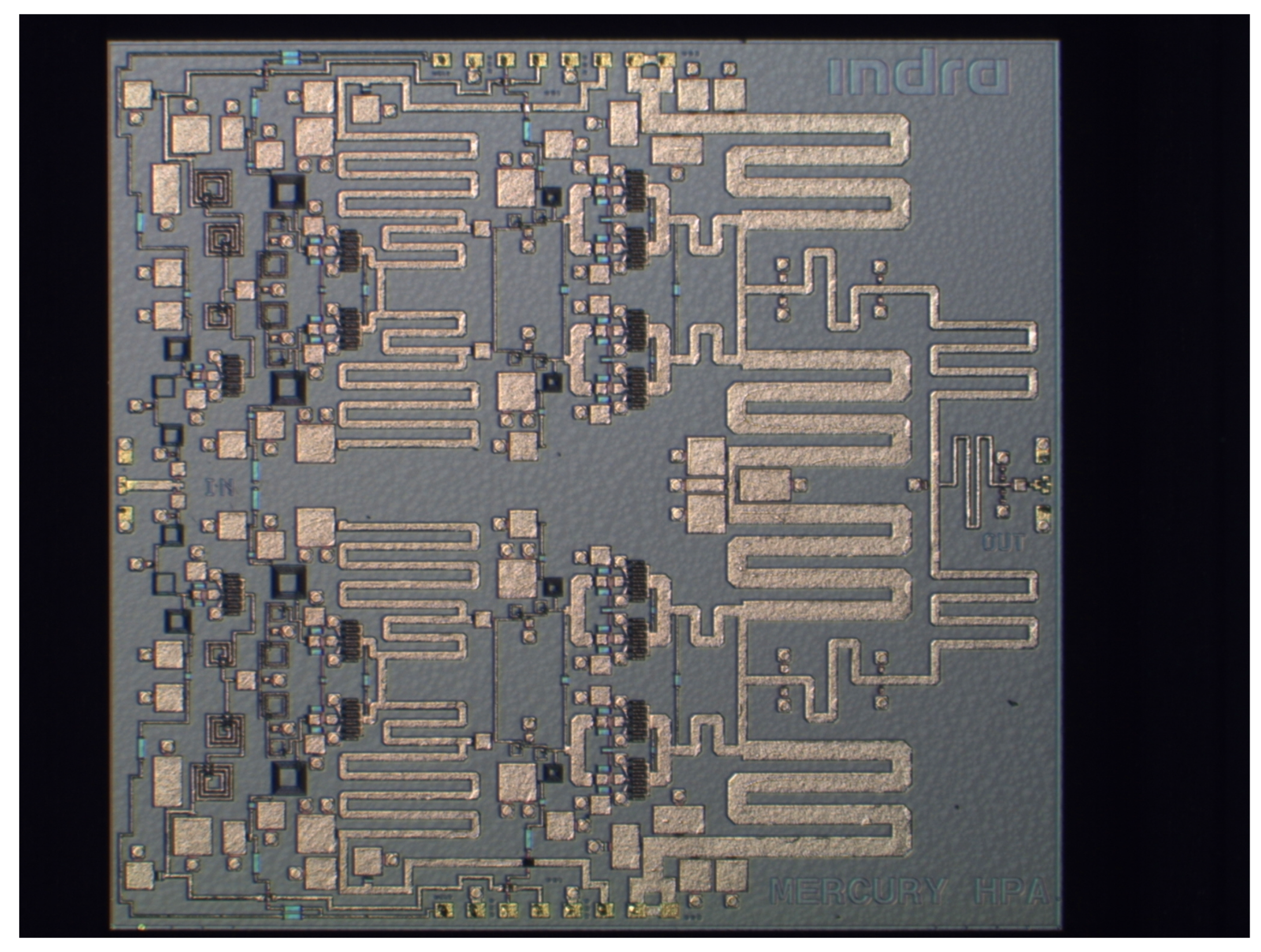
Figure 7 shows a photomicrograph of the constructed HPA MMIC.
3.1. Stability Analysis
Theoretically, the analysis of any stability criteria [
53,
54] can be usefully applied to verify the unconditional stability of the two-port network in the small-signal regime. Unfortunately, as described in numerous articles [
50,
55,
56], a high-frequency HPA (power amplifier) cannot be adequately modeled as a two-port network. This is because an HPA MMIC has a complex structure with multiple bias ports and paths for the RF signal. This leads to, as predicted by Platzer [
55], oscillations or instabilities that cannot be adequately detected solely with the k-stability test from the small-signal S-parameters of two-port networks. This requirement is necessary but not sufficient because compliance with it does not guarantee circuit stability. It is well known [
53,
54,
55,
56] that if the final circuit simulation results in a circuit that meets the classical stability condition, then the
factor [
54] obtained will be greater than 1 in the amplifier’s operating frequency band, but it does not assure the instabilities of the internal feedback paths.
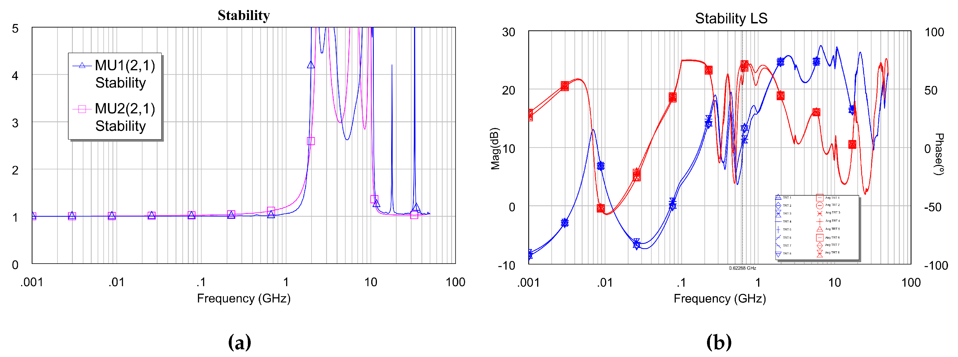
To ensure the stability of the designed HPA MMIC, , in this case a stability criterion in LS (large-signal) is applied, identifying pole-zero locations at various nodes of the HPA MMIC and for different power levels. Therefore, to guarantee the unconditional stability of the amplifier and ensure that no instabilities appear, stability analyses are conducted in both small and large signal domains, as shown in
Figure 8.
4. HPA Measurement
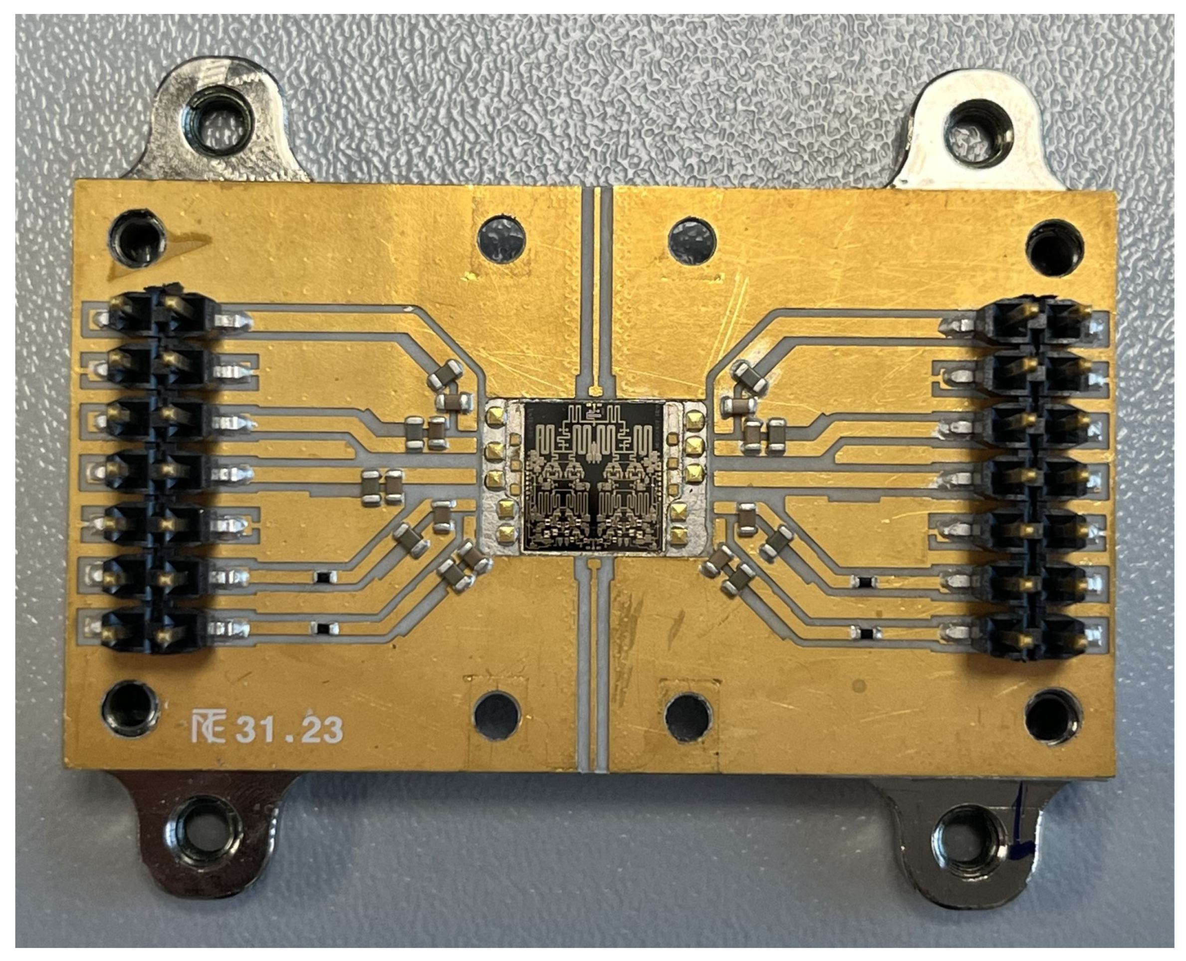
In this section, the results obtained from the measurements are presented and compared with the simulations conducted in AWR for the designed HPA MMIC. "On-wafer" measurements of the HPA have been carried out by the LEONARDO Foundry. The article shows the two sets of measurements conducted “On Wafer” and “On jig”. For the “On jig” measurement, the HPA MMIC has been mounted on a carrier by
INDRA company , as shown in the photograph in
Figure 9.
The HPA MMIC was mounted for “On jig” measurements on a board specifically designed for measuring these circuits. This board was constructed on a Rogers 3003 substrate ( = 2.2, h = 5 mil) from Rogers Corporation. The input and output connectors chosen were ELF-KN 2.92 mm Edge Launch connectors from Southwest Microwave. Once the circuit was mounted on the board, interconnections between the MMIC and the board were made using wire bondings. The MMIC bonding wires have a length close to 160 m at the inputs and outputs, with a diameter of 25.4 m. The distance between the chip’s input/output line and the board is approximately 70 m.
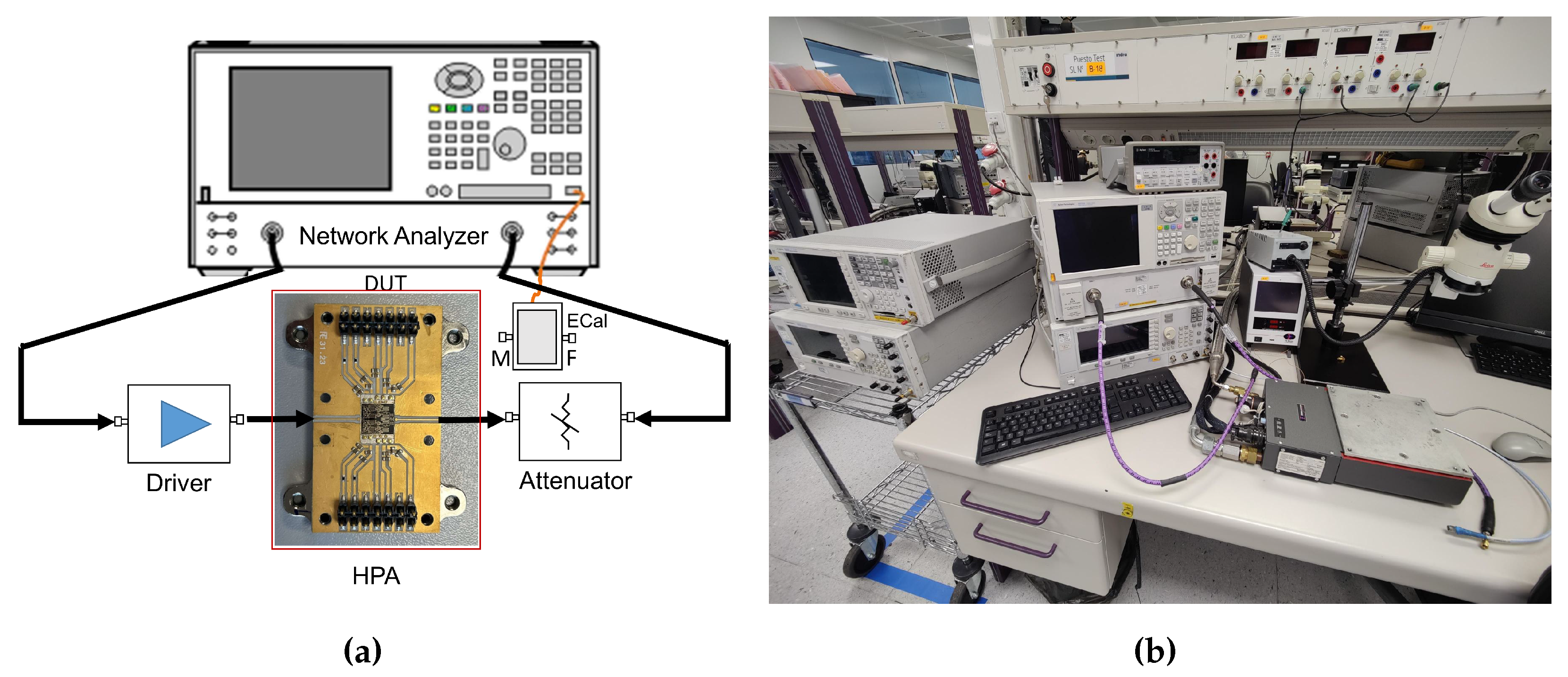
Next, once mounted as previously mentioned, the circuit is characterized and measured. The circuit assembly is arranged according to the layout shown in
Figure 10.
Figure 10 shows the instruments used in the measurement setup.
For better clarity, the measurements conducted are presented in two subsections, corresponding to small-signal measurements and large-signal measurements.
4.1. Small-Signal Measurements
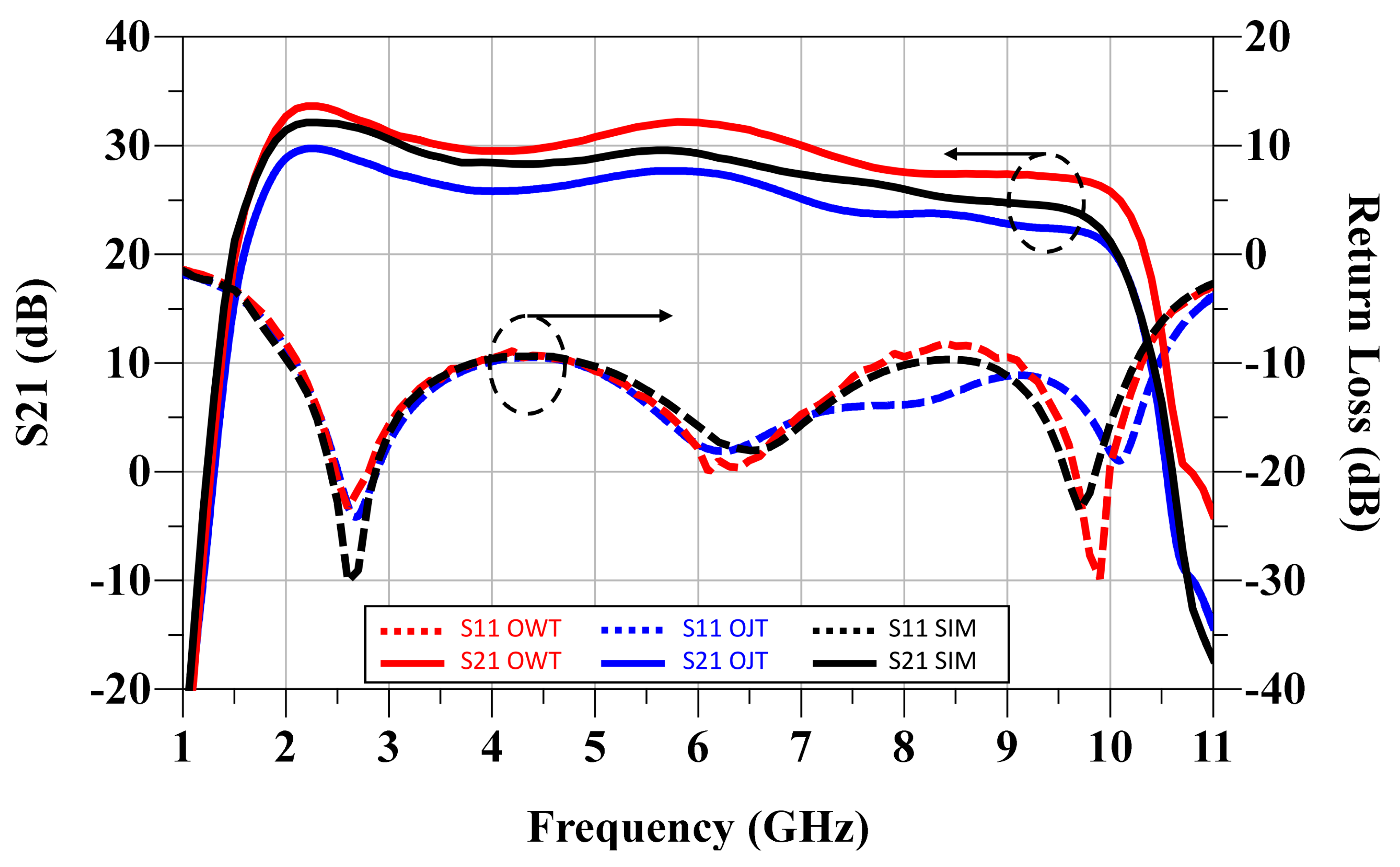
Firstly, although small-signal measurements are less important for power amplifiers compared to other circuits such as low-noise amplifiers (LNAs) or drivers, they were conducted to verify the accuracy of the design. The S-parameters were measured using the Keysight PNA-X vector network analyzer with electronic calibration. The return loss values at the input and output are greater than 11 dB,
dB, and
dB. These values indicate an acceptable level in the port matching for the input and output of the HPA. Additionally, as observed in the
Figure 11, there is excellent agreement between the simulation and the measured results.
However, as previously mentioned, these values lack the importance they hold for other RF/MW devices. Let’s recall the fundamental role and function of an HPA, which is to operate in large-signal conditions. This implies that the amplifiers function in a nonlinear regime where the assessment of return losses is not as critical.
The small-signal measurement of the HPA was completed via Keysight vector network analyzer (VNA) N5242 B (Keysight Technologies, Santa Rosa, CA, USA).
Figure 8 demonstrates the measured S-parameters in comparison to the simulated ones. It is evident that the measurements and simulations are in good consistency. The amplifier achieves a small-signal gain of 24–25.5 dB with gain flatness less than ±0.75 dB across the frequency range of 2–6 GHz. The measured input and output return losses are better than 14.5 and 10 dB, respectively, achieving good input and output matching
4.2. Large-Signal Measurements
RF and microwave HPAs play a crucial role in the output stages of RF and microwave chains in both communication systems and electronic warfare. One of the measurements that truly characterize the HPA correspond to large-signal measurements. To optimize system performance, it is important to understand its key performance metrics are and , as primary parameters.
In summary, understanding and optimizing and are essential for the efficient and effective design of RF and microwave amplifiers in a wide range of applications.
Performance Evaluation: These metrics provide a direct assessment of the amplifier’s performance in terms of the amount of output power it can deliver and the efficiency with which it converts input power into output power
Energy Efficiency: is especially important as it indicates how much input energy is effectively converted into useful output energy. High energy efficiency is crucial for minimizing power consumption and maximizing battery life.
Design and Optimization: Understanding these metrics is essential for designing and optimizing RF and microwave systems. It allows engineers to make informed decisions about component selection, circuit topologies, and biasing strategies to achieve desired performance levels.
Impact on Signal Quality: and can also impact the quality of the output signal. High output power can improve transmission capacity and signal coverage, while high efficiency can reduce distortion and improve signal fidelity
As previously mentioned, measurements performed both “On wafer” and “On jig” are presented, along with their comparison with the simulated results. For the measurements, the test bench and instrumentation shown in
Figure 10 have been used. Besides, as explained before, the jig structure has parasitic effects that cannot be de-embedded and, added to the thermal effect of the CW excitation, makes the gain on the jig lower than the simulated or the OW ones.
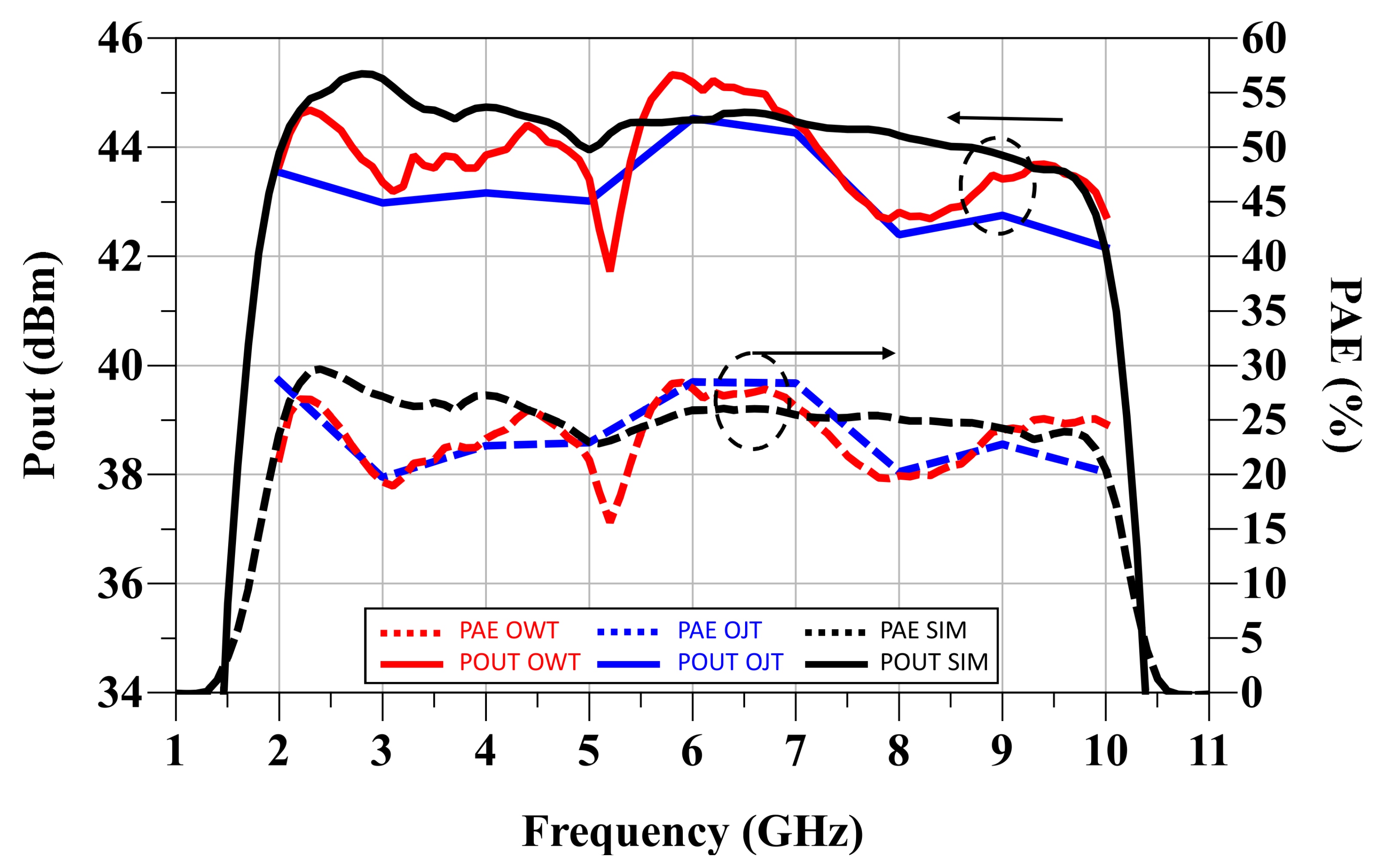
The large-signal measurement was measured using Vector Network analyzer (VNA) N5242 B Keysight (Keysight Technologies, Santa Rosa, CA, USA), drive amplifier,and attenuator. A under driving CW signal. The measured saturated output power (Pout), PAE, and gain against frequency are demonstrated in
Figure 12. In this case, the input power (Pin) is fixed as 23 dBm. The output power varies from 45.7 to 43 dBm, and PAE are within 30–20%, respectively, The lack of power in the on-jig measurements in comparison with the on-wafer measurements can be explained due to the thermal effect.
The
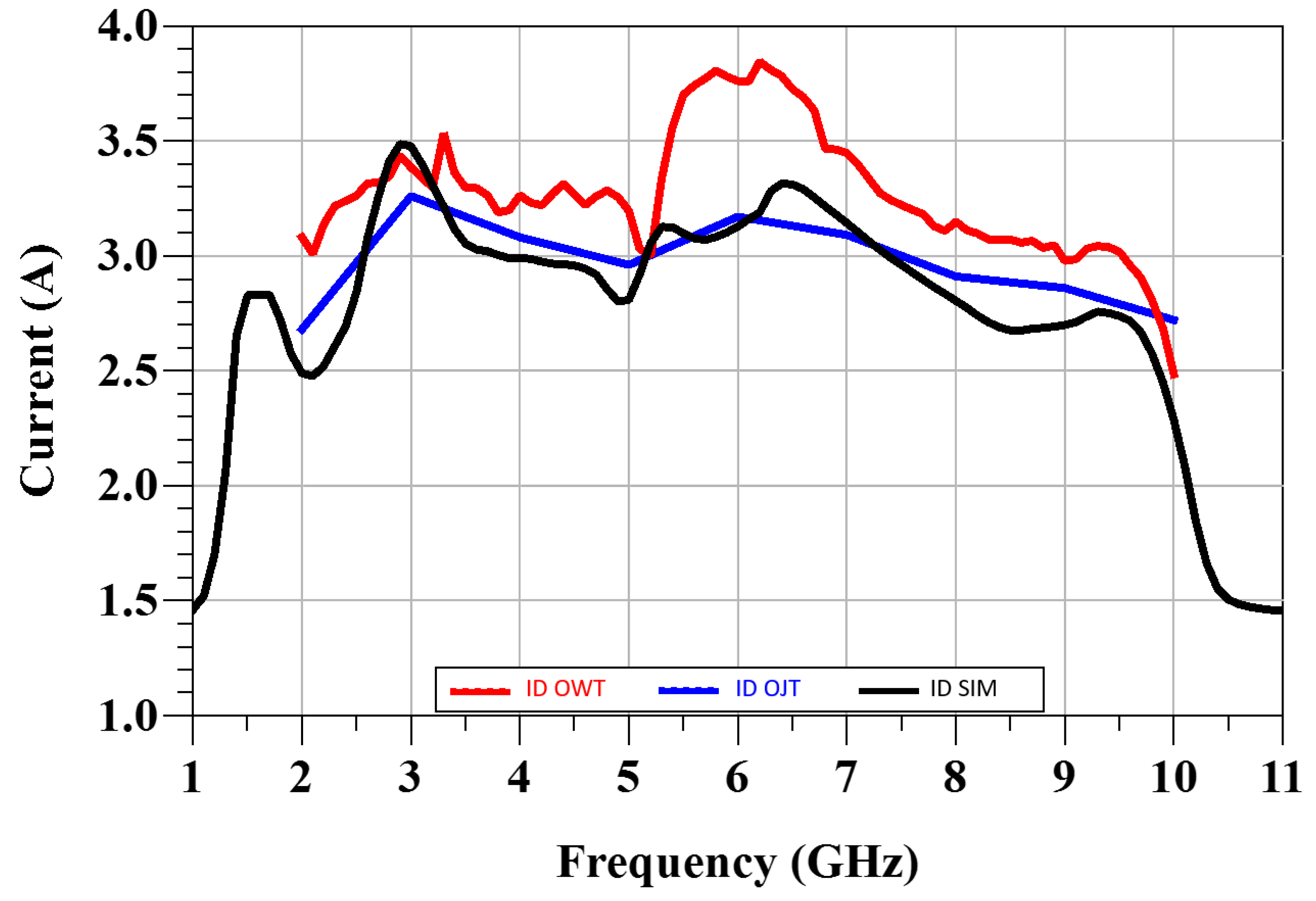
Figure 13 shows the measurement of the current consumed by the MMIC with an input power of 23 dBm. It can be observed that there is great agreement between the simulation and the measurements.
4.3. Sumary of Performances
After conducting small and Large Signal measurements, the results are presented in
Table 4, where we can compare and observe the compliance with almost all design specifications, with the exception of IRL, which is slightly lower. However, the MMIC is still valid as HPA suitable as a first approximation to the initial specifications.
5. Discussion
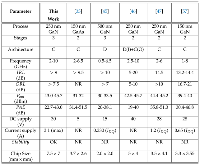
Table 5 shows a comparison of the performance of the designed HPA with other published MMIC HPAs in similar frequency bands to the specified requirements. In recent years, to meet the high demand for broadband work and increased performance in applications below 20 GHz, high-efficiency broadband amplifiers have been extensively studied. They have been compared with various amplifiers starting with GaAs technology [
33], where its lower power level compared to GaN technology is evident. Next, it has been compared with various GaN HPAs with higher broadband power levels manufactured to cover similar frequency and power ranges as specified, maintaining output power levels in the order of watts. In [
45], a non-uniformly distributed GaN power amplifier from 0.5 to 6.5 GHz was presented with a small chip area to achieve output power greater than 30 dBm and a PAE of 20-38.1%. In [
46], a GaN power amplifier from 2.5 to 10.5 GHz was implemented with distributed amplifier stages at the input and a reactively tuned corporate stage at the output to achieve saturated output power of 18–37 W and a PAE of 19–40%. In [
47], an interesting work is shown, where an HPA MMIC covering the 2 to 6 GHz band and an output power of 10 watts with a PAE value exceeding 35%.
Finally, the designed HPA MMIC has been compared with a commercial GaN power amplifier from Qorvo [
57] with relatively similar performance. It is worth noting that although the proposed design has a larger size than the referenced ones, this is largely due to the output power value. Regarding gain and PAE, it should be noted that the value is in line with the current state-of-the-art and as of the date of this article.
The obtained results demonstrate that the performance of the HPA is satisfactory compared with the performance of other HPA reported in the literature on this topic. Table 5 shows a comparison of the proposal of this article with five very good proposals that can be considered references in the field of HPA design. 6. Conclusion
A high-power amplifier has been designed and measured in the 2 to 10 GHz frequency band for MFRF systems using Leonardo’s 250 nm GaN technology process (LDO GN25). This amplifier represents a significant advancement in communication and radar system development, offering an efficient and powerful solution for multifunctional applications.
The meticulous design and precise implementation of GaN technology allow the amplifier to achieve more than 43 dBm of output power, setting a new standard in terms of performance and transmission capability. Additionally, the power added efficiency exceeds 20 %, ensuring cost-effective and environmentally friendly operation.
In terms of power consumption, the MMIC exhibits a drain current consumption of less than 4 A across the frequency band, making it highly energy-efficient. Detailed characterization of the amplifier reveals excellent agreement between theoretical simulations and measurements, validating the accuracy and reliability of the design.
During on-wafer measurements, even higher gain is observed than predicted by simulations, suggesting even greater potential for this amplifier under real operating conditions. However, large signal results show slightly lower output power than simulations, which may be attributed to a thermal effect due to heat generated during operation.
In summary, this HPA represents an ideal option for integration into future TRMs for AESA systems. Its ability to deliver high levels of output power, energy efficiency, and reliability makes it a versatile and adaptable solution for a wide range of applications, including radar, electronic warfare, and communications, all within the same system.
Author Contributions
Conceptualization: V.G.-P. and J.L.J.-M. ; methodology: V.G.-P. and J.L.J.-M; software: A.P.-P. and A.F.-E.; validation and simulation: V.G.-P. and J.L.J.-M.; formal analysis: V.G.-P. and J.L.J.-M.; resources: A.F.-G., E.O.-G., J.M.-P. and J.S.-M.; writing original draft: A.P.-P and J.M.-P.; writing, review and editing: A.F.-E. and J.M.-P.; supervision: A.F.-E., V.G.-P and E.O.-G.; chip acquisition: A.F.-E.. A.P.-P and J.M.-P; measurements: A.F.-E., A.P.-P and E.O.-G. All authors have read and agreed to the published version of the manuscript. Authorship was limited to those who contributed substantially to the work reported
Funding
This project has received funding from the European Union’s Preparatory Action on Defence Research under grant agreement No. 882407.
Institutional Review Board Statement
Not applicable.
Informed Consent Statement
Not applicable.
Data Availability Statement
Not applicable
Acknowledgments
The authors would like to thank European Defence Agency (EDA) and European Commission (EC) for supporting CROWN project, and Virginia Bueno Fernandez and Marıa Luz Gil Heras, Indra Sistemas, Madrid, Spain for their assistance.
Conflicts of Interest
The authors declare no conflict of interest.
References
- Jones, G. , Egan J. and Rosenbach E. “Advancing in Adversity: Ukraine’s Battlefield Technologies and Lessons for the U.S.”, Belfer Center, Harvard Kennedy School, Monterey, CA, USA, 2023.
- Boot, M. , “The Ukraine war is revolutionizing military technology. Whoever masters it wins”, The Washington Post, 23, September 2023.
- Huizing, A. G.; “Wideband, vs. multiband trade-offs for a scalable multifunction RF system,” IEEE International Radar Conference, 2005., Arlington, VA, USA, 2005, pp 155-160. [CrossRef]
- Moo, P. W. and DiFilippo, D. J.; “Overview of Naval Multifunction RF Systems,” 2018 15th European Radar Conference (EuRAD), Madrid, Spain, 2018, pp. 178-181. [CrossRef]
- Kellett,J. ; Dawber, W.; Wallace, W. and Branson, J.; “Multifunction Maritime Radar and RF Systems—Technology Challenges and Areas of Development,” in IEEE Aerospace and Electronic Systems Magazine, vol. 37, no. 4, pp. 6-20, 1 April 2022. [CrossRef]
- M. Brandfass, M.; Moeller, T. and Weidmann,K.; "“Multifunctional Radar and Data Link Functions for Dual Use Applications,” in 2023 IEEE International Radar Conference (RADAR), Sydney, Australia, 2023, pp. 1-6. [CrossRef]
- Martel, C.; Castanet, L,: Jeuland, H.; Brouard, P. and Bolioli, S.; “CROWN Project: a Wideband Radiating Array Antenna for EM Multifunction System”. <italic>2023 IEEE Conference on Antenna Measurements and Applications (CAMA)</italic>, Genoa, Italy, 2023, pp. 209-211. [CrossRef]
- Heras, M. L. G.; Garcia, A. C.; Soriano, J. C.; De La Haba, J. L. G.; Le Roy-Naneix, I.; Kemkemian, S.; Thorsell, M.; Brandfass, M. ; Brouard,P.; T. Boman, Durst, S.; Nanni, A.; De Wit, J. J.; Calfa, U. and Sakalaset,M.; “CROWN Project, towards a European Multifunction AESA system,” 22022 IEEE International Symposium on Phased Array Systems & Technology (PAST), Waltham, MA, USA, 2022, pp. 1-8. [CrossRef]
- CROWN (2021), “Crown Project. [Online]”. Available: https://www.crown-padr.eu/.
- N. Rao, A. Parfitt, A. Dadello, D. Ward and T. Bird, “A Low Noise Ka-Band Down Converter for Space Applications”, 2000 30th European Microwave Conference, Paris, France, 2000, pp. 1-4. [CrossRef]
- Jae-Woo Park, S. Mohammadi, D. Pavlidis, C. Dua, J. L. Guyaux and J.. -C. Garcia, “GaInP/GaAs HBT broadband monolithic transimpedance amplifiers and their high frequency small and large signal characteristics,” 1998 IEEE Radio Frequency Integrated Circuits (RFIC) Symposium. Digest of Papers (Cat. No.98CH36182), Baltimore, MD, USA, 1998, pp. 179-182. [CrossRef]
- E. Martins, M. V. G. Gomes, E. M. Bastida and J. W. Swart, “Design of a LNA and a Gilbert cell mixer MMICs with a GaAs PHEMT technology,” 1999 SBMO/IEEE MTT-S International Microwave and Optoelectronics Conference, Rio de Janeiro, Brazil, 1999, pp. 267-270 vol. 1. [CrossRef]
- H. Hamada et al., “300-GHz 120-Gb/s wireless transceiver with highoutput-power and high-gain power amplifier based on 80-nm InP-HEMT technology,” in Proc. IEEE BiCMOS Compound Semiconductor Integr. Circuits Technol. Symp. (BCICTS), Nov. 2019, pp. 1–4.
- H. Zhang, Q. Li, and L. Xu, “A K-band Single-to-Differential Broadband Low Noise Amplifier with LC Anti-interference Network,” 2021 International Conference on Microwave and Millimeter Wave Technology (ICMMT), 2021, pp. 1-3. [CrossRef]
- Soubercaze-Pun, G, Tartarin, JG, Bary, L, Rayssac, J, Delage, S, and Graffeuil, G. “Robust GaN Electronics for Highly Reliable BF and RF Analog Systems in Aerospace Applications,” Proceedings of the CANEUS 2006: MNT for Aerospace Applications, Toulouse, France. August 27–September 1, 2006. pp. 81-87. ASME. [CrossRef]
- D. Ueda, “Status Quo and trends of GaN power devices”, 2013 IEEE International Reliability Physics Symposium (IRPS), Monterey, CA, USA, 2013, pp. 3C.2.1-3C.2. [CrossRef]
- P. Igic, S. Faramehr and K. Kalna, “GaN technology for power RF applications: Present reliability roadblocks and future trends”, 2014 29th International Conference on Microelectronics Proceedings - MIEL 2014, Belgrade, Serbia, 2014, pp. 77-80. [CrossRef]
- A. Margomenos et al., “Novel packaging, cooling and interconnection method for GaN high performance power amplifiers and GaN based RF front-ends”, 2012 7th European Microwave Integrated Circuit Conference, Amsterdam, Netherlands, 2012, pp. 615-618.
- A. S. Verma, A. K. Jaiswal, M. Kumar, G. Nigam and S. K. Srivastava, “Measurement of reliability and availability of satellite communication links: Progress and challenges,”, T2013 International Conference on Intelligent Systems and Signal Processing (ISSP), Vallabh Vidyanagar, India, 2013, pp. [CrossRef]
- ITU, “Reliable space services: Why and how?”, https://www.itu.int/hub/2021/10/reliable-space-services-why-and-how/.
- Miranda, R.F.; Barriquello, C.H.; Reguera, V.A.; Denardin, G.W.; Thomas, D.H.; Loose, F.; Amaral, L.S. Review of Cognitive Hybrid Radio Frequency/Visible Light Communication Systems for Wireless Sensor Networks. Sensors 2023, 23, 7815. [Google Scholar] [CrossRef] [PubMed]
- Campbell, C.F.; Balistreri, A.; Kao , M. -Y.; Dumka, D. C. and Hitt, J.; “GaN Takes the Lead,” in IEEE Microwave Magazine, vol. 13, no. 6, pp. 44-53, Sept.-Oct. 2012. [CrossRef]
- Dutta, R.; Tamang, T.; Paul, P. and Paitya, N.; “Comparative Study of AlGaN/GaN, InAlN/GaN and AlGaAs/GaAs based High Electron Mobilty Transistors Using Silvaco for High-Frequency Applications,” 2020 4th International Conference on Trends in Electronics and Informatics (ICOEI)(48184), Tirunelveli, India, 2020, pp. 137-142. [CrossRef]
- M. Micovic et al., “GaN MMIC technology for microwave and millimeter-wave applications”, IEEE Compound Semiconductor Integrated Circuit Symposium, 2005. CSIC ’05., Palm Springs, CA, USA, 2005, pp. 3. [CrossRef]
- M. Sudow et al., “An AlGaN/GaN HEMT-Based Microstrip MMIC Process for Advanced Transceiver Design,” in IEEE Transactions on Microwave Theory and Techniques, vol. 56, no. 8, pp. 1827-1833, Aug. 2008. [CrossRef]
- R. Rieger, A. Klaaßen, P. Schuh and M. Oppermann, “GaN based wideband T/R module for multi-function applications,” 2015 European Microwave Conference (EuMC), Paris, France, 2015, pp. 514-517. [CrossRef]
- A. Salvucci et al., “Single MMIC receivers for C-band T/R module in 0.25 μm GaN technology,” 2018 14th Conference on Ph.D. Research in Microelectronics and Electronics (PRIME), Prague, Czech Republic, 2018, pp. 201-204. [CrossRef]
- M. van Heijningen et al., “C-Band Single-Chip Radar Front-End in AlGaN/GaN Technology”, in IEEE Transactions on Microwave Theory and Techniques, vol. 65, no. 11, pp. 4428-4437, Nov. 2017. [CrossRef]
- A. De Padova, P. E. Longhi, S. Colangeli, W. Ciccognani and E. Limiti, “Design of a GaN-on-Si Single-Balanced Resistive Mixer for Ka-band Satcom”, in IEEE Microwave and Wireless Components Letters, vol. 29, no. 1, pp. 56-58, Jan. 2019. [CrossRef]
- Tao, R.; Berroth, M.; Wang, Z.G.: “Monolithically integrated CMOS current-mode transimpedance preamplifier”, Electronics Letters, 2003, 39, (25), p. 1772-1774, DOI: 10.1049/el:20031174 IET Digital Library, https://digital-library.theiet.org/content/journals/ 10.1049/el_20031174.
- S. J. Mahon et al., “Broadband integrated millimeter-wave up- and down-converter GaAs MMICs”, <italic>in IEEE Transactions on Microwave Theory and Techniques</italic>, vol. 54, no. 5, pp. 2050-2060, May 2006. [CrossRef]
- G. W. de Jong, D. M. W. Leenaerts and E. van der Heijden, “A Fully Integrated Ka-Band VSAT Down-Converter”, <italic>in IEEE Journal of Solid-State Circuits</italic>, vol. 48, no. 7, pp. 1651-1658, July 2013. [CrossRef]
- Ding, X. and ; Zhang, L. “A High-Efficiency GaAs MMIC Power Amplifier for Multi-Standard System.” in IEEE Microwave and Wireless Components Letters, vol. 26, no. 1, pp. 55-57, Jan. 2016. [Google Scholar] [CrossRef]
- Xiaofan Wen, Tongsheng Xia, Huan He and Jungang Miao, “A low noise down converter MMIC for synthetic aperture radiometer application”, 2016 IEEE International Conference on Microwave and Millimeter Wave Technology (ICMMT), Beijing, 2016, pp. [CrossRef]
- B. Ding, S. Yuan, C. Zhao, L. Tao and T. Tian, “A Ka Band FMCW Transceiver Front-End With 2-GHz Bandwidth in 65-nm CMOS,” in IEEE Transactions on Circuits and Systems II: Express Briefs, vol. 66, no. 2, pp. 212-216, Feb. 2019. [CrossRef]
- F. Li and Y. Wu, “Ka-band Single-chip GaAs PHEMT Transceiver MMIC for Ranging FMCW Radar, ” 2019 International Conference on Microwave and Millimeter Wave Technology (ICMMT), Guangzhou, China, 2019, pp. 1-3. [CrossRef]
- T. Takenaka, A. Miyazaki, H. Matsuura and H. Iwaoka, “MMIC’s for an integrated RF spectrum analyzer front end,” in IEEE Transactions on Instrumentation and Measurement, vol. 44, no. 3, pp. 716-719, June 1995. [CrossRef]
- E.A.M. Klumperink, F. Bruccoleri, P. Stroet, and B. Nauta, “Amplifiers Exploiting Thermal Noise Canceling: A Review,” 12th Gallium Arsenide and other compound semiconductor Application Symposium (GAAS), Amsterdam, NL, Horizon House Publications Ltd, 2004. pp. 371-374.
- R. Gharpurey, “A broadband low-noise front-end amplifier for ultra wideband in 0.13 μm CMOS,” Proceedings of the IEEE 2004 Custom Integrated Circuits Conference (IEEE Cat. No.04CH37571), Orlando, FL, USA, 2004, pp. 371-374. [CrossRef]
- A. Tessmann, I. Kallfass, A. Leuther, H. Massler, M. Schlechtweg and O. Ambacher, “Metamorphic MMICs for Operation Beyond 200 GHz,” 2008 European Microwave Integrated Circuit Conference, Amsterdam, Netherlands, 2008, pp. 210-213. [CrossRef]
- A. Leuther et al., “Metamorphic HEMT technology for low-noise applications,” 2009 IEEE International Conference on Indium Phosphide & Related Materials, Newport Beach, CA, USA, 2009, pp. 188-191. [CrossRef]
- C. Xie and A. Pavio, “Development of GaN HEMT based High Power High Efficiency Distributed Power Amplifier for Military Applications”. MILCOM 2007 - IEEE Military Communications Conference, Orlando, FL, USA, 2007, pp. 1-4. [CrossRef]
- P. Schuh et al., “GaN MMIC based T/R-Module Front-End for X-Band Applications”, 2008 European Microwave Integrated Circuit Conference, Amsterdam, Netherlands, 2008, pp. 274-277. [CrossRef]
- B. Mallet-Guy, L. Darcel, J. -P. Plaze and Y. Mancuso, “First 0.25µm GaN MMICs dedicated to compact,wideband and high SFDR receiver,” in 2012 7th European Microwave Integrated Circuit Conference, Amsterdam, Netherlands, 2012, pp. 329-332.
- Zhou, X.; Roy, L.; Amaya, R.E. “1 W, Highly Efficient, Ultra-Broadband Non-Uniform Distributed Power Amplifier in GaN,” in IEEE Microwave and Wireless Components Letters, vol. 23, no. 4, pp. 208-210, April 2013. [CrossRef]
- Kamioka, J.; Hangai, M.; Komaru, R.; Morimoto, T.; Kamo, Y.; Shinjo, S. Over 20 W 2.5 to 10.5 GHz wideband two-stage GaN MMIC power amplifier with distributed and reactively-matched amplifier stages. In Proceedings of the 49th European Microwave Conference, Paris, France, 13 October 2019.
- Hu, L.; Liao, X.; Zhang, F.; Wu, H.; Ma, S.; Lin, Q.; Tang, X. “A Wideband High-Efficiency GaN MMIC Power Amplifier for Sub-6-GHz Applications”. Micromachines 2022, 13, 793. [Google Scholar] [CrossRef] [PubMed]
- Cadence. RF / Microwave Design with AWR Software. Available online: https://www.cadence.com/en_US/home/tools/system-analysis/rf-microwave-design.html (accessed on 22 September 2023).
- Keysight. PathWave Advanced Design System (ADS). Available online: https://www.keysight.com/us/en/products/software/pathwave-design-software/pathwave-advanced-design-system.html (accessed on 20 September 2023).
- González-Posadas, V.; Jiménez-Martín, J.L.; Parra-Cerrada, A.; Espinosa Adams, D.; Hernandez, W. “Stability, Mounting, and Measurement Considerations for High-Power GaN MMIC Amplifiers”. Sensors 2023, 23, 9602. [Google Scholar] [CrossRef] [PubMed]
- I.D. Robertson, S. Lucyszyn, “RFIC and MMIC Design and Technology”. Institution of Electrical Engineers, 2001. [CrossRef]
- Marsh, S. “Practical MMIC Design”, in 1st ed. Norwood: Artech House, 685 Canton Street Norwood, MA 02062 2006.
- Woods, D. , “Reappraisal of the unconditional stability criteria for active 2-port networks in terms of s parameters,”IEEE Transactions on Circuits and Systems, vol. 23, no. 2, pp. 73–81, February 1976.
- Edwards, M. L. and Sinsky, J. H., “A new criterion for linear 2-port stability using a single geometrically derived parameter,” IEEE Transactions on Microwave Theory and Techniques, vol. 40, no. 12, pp. 2303–2311, Dec 1992.
- Platzker, A. , Struble, W., and Hetzler, K. T. “Instabilities diagnosis and the role of k in microwave circuits,” in 1993 IEEE MTT-S International Microwave Symposium Digest, pp. 1185–1188 vol.3, June 1993.
- Struble, W. and Platzker A., “Instabilities diagnosis and the role of k in microwave circuits,” in 15th Annual GaAs IC Symposium, pp. 251–254, Oct 1993.
- QPA 1003D Comercial Device, “Datasheet QPA 1003D”, Qorvo Inc 2024. https://www.qorvo.com/products/p/QPA1003D|hashkeytag|documents.
|
Disclaimer/Publisher’s Note: The statements, opinions and data contained in all publications are solely those of the individual author(s) and contributor(s) and not of MDPI and/or the editor(s). MDPI and/or the editor(s) disclaim responsibility for any injury to people or property resulting from any ideas, methods, instructions or products referred to in the content. |
© 2024 by the authors. Licensee MDPI, Basel, Switzerland. This article is an open access article distributed under the terms and conditions of the Creative Commons Attribution (CC BY) license (http://creativecommons.org/licenses/by/4.0/).
