
Submitted:
19 June 2024
Posted:
20 June 2024
You are already at the latest version
Abstract
Using the example of III-V nitrides crystallizing in a wurtzite structure (GaN, AlN, InN), this review presents the special role of hydrostatic pressure in studying semiconductor properties. Starting with a brief description of high pressure techniques for growing bulk crystals of nitride compounds, we focus on the use of hydrostatic pressure techniques in both experimental and theoretical investigations of special properties of nitride compounds, their alloys and quantum structures. The band gap pressure coefficient is one of the most important parameters in semiconductor physics. Trends in its behavior in nitride structures, together with trends in pressure-induced phase transitions, are discussed in the context of the behavior of other typical semiconductors. Using InN as an example, the pressure-dependent effects typical of very narrow bandgap materials, such as conduction band filling or effective mass behavior, are described. Interesting aspects of bandgap bowing in In-containing nitride alloys, including pressure and clustering effects, are discussed.Hydrostatic pressure also plays an important role in the study of native defects and impurities, as illustrated by the example of nitride compounds and their quantum structures. Experiments and theoretical studies on this topic are reviewed. Special attention is given to hydrostatic pressure and strain effects in short periods nitride superlattices. The explanation of the discrepancies between theory and experiment in the optical emission and its pressure dependence from InN/GaN superlattices led to the well-documented conclusion that InN growth on the GaN substrate is not possible. The built-in electric field present in InGaN/GaN and AlGaN/GaN heterostructures crystallizing in wurtzite lattice can reach several MV/cm, leading to drastic changes in the physical properties of these structures and related devices. It is shown how hydrostatic pressure modifies these effects and helps to understand their origin.
Keywords:
Hydrostatic pressure
; semiconductors
; III-V nitrides
; optoelectronic devices
1. Introduction
To illustrate the importance of hydrostatic pressure as a research tool in semiconductor physics, this review describes and discusses its role in the study of nitride compounds, their alloys, and heterostructures such as quantum wells and superlattices. We will also briefly present the related properties of Light Emitting Diodes (LEDs) and Laser Diodes (LDs).
Our focus is on nitrides that crystallize in the hexagonal wurtzite structure (InN, GaN and AlN). They form a distinct subset of III-V compounds characterized by high ionicity, short bond lengths, low compressibility, and high thermal conductivity. Covering a wide light spectrum from 0.7 eV (InN) [1] to 6.03 eV (AlN) [2], they have become one of the most important materials in optoelectronics forming the basis of visible and ultraviolet (UV) LEDs and LDs. In addition, these materials have also become increasingly important in the electronics industry, enabling the development of devices such as high-power, high-voltage transistors and high electron mobility transistors (HEMTs).
Hydrostatic pressure is a very important tool in the study of nitride materials, starting with a crucial role in their growth techniques, as they are prone to decomposition at high temperatures [3,4]. The high pressure has revealed significant differences in lattice stability under pressure between GaN, AlN and InN compounds, confirming the high ionicity of these materials. Nitride semiconductors have several interesting and atypical properties. Of these, InN is the most unique. The narrow band gap of InN gives rise to a number of interesting physical effects. Specific features of InN under pressure are worth mentioning, such as the pressure dependence of the effective mass and the effect of conduction band filling. Furthermore, the hydrostatic pressure study of the band structure of semiconductor alloys reveals interesting effects, as shown by the example of In-containing nitride alloys such as InGaN and InAlN. It is shown how the bandgap values depend on the geometrical arrangement of the atoms in the crystal, and how it influences the band gap bowing and the bowing of the band gap pressure coefficients [5,6,7]. The issues presented above will be discussed in Chapter II of this review.
Chapter III then describes high-pressure studies of native defects and impurities in nitride compounds. High pressure experiments and theoretical studies have contributed to a better understanding of the physics of impurities and native defects in nitrides in particular and in all III-V semiconductors in general (e.g., GaAs doped with Si, Sn or Ge). Regarding nitride semiconductors, special interest began in the nineties of the last century with DX states (deep states with high relaxation energy) involving oxygen in GaN [8,9] and DX-like defects of unknown origin in n-type InN [10,11]. At the same time, theoretical studies of the DX states in nitrides, including their structural aspects [12,13], have provided highly valuable information and introduced further microscopic models describing their properties. Chapter IV discusses the important role of hydrostatic pressure in the study of nitride QWs and SLs. This chapter presents the role of high pressure in identifying and better understanding the mechanisms responsible for the effective emission of LEDs and LDs, which can be used for further optimization of the parameters of these optoelectronic devices. Strain effects and related Quantum Confined Stark Effect (QCSE) [14] in quantum structures are described. It is shown how the high pressure contributed to the well-documented conclusion that InN growth on the GaN substrate is not possible [15,16,17]. In Chapter V, the role of hydrostatic pressure in determining the properties of optoelectronic devices will be briefly described along with some perspectives for future research in the field of the present review. Finally, Chapter VI summarizes the main points of the review.
2. High Pressure Effects in Nitride Compounds and Alloys
2.1. High Pressure in Crystal Growth
High pressure can affect the physical properties of semiconductor crystals and the material systems containing them. The latter means pressure-induced changes in free energies in multiphase systems thus modifying the stability range of the system components. The III-N compounds are relatively strongly bonded crystals making them thermally and chemically stable and also inducing their high melting temperatures. On the other hand, in the systems of the III-N constituents: III group metals and N2 gas, an extremely strong bond in the N2 molecule lowers the free energy of the constituents leading to thermal decomposition of the III-N crystals at temperatures lower than their expected melting points. High pressure of nitrogen is needed to extend the III-N’s stability range thus suppressing their decomposition [3,4]. This situation is illustrated for GaN, in Figure 1.
The extreme p-T conditions expected (the melting curves are still unknown!) for melting of the III-N compounds [4,18,19] make bulk crystal growth from stoichiometric melts technically unfeasible. The N2 pressure required for the stability of AlN, GaN and InN at high temperatures is very sensitive to the corresponding bonding energies in the crystals. The differences in the equilibrium N2 pressure over III-N crystals reach several orders of magnitude as illustrated in Figure 2.
It has direct consequences for the development of crystal growth methods for these extremely important materials:
AlN
As it follows from Figure 2, AlN is thermally stable at atmospheric pressure even at very high temperatures [20]. The most suitable method for growing bulk AlN crystals is the physical vapor transport (PVT) method at temperatures above 2000oC which allows the fabrication of 2-inch substrates of high structural quality in terms of low dislocation density [21,22]. However, owing to the high-temperature conditions during growth, the concentration of point defects is high, which leads to increased optical absorption. As an alternative, the vapor phase epitaxy (HVPE) process involving ammonia as an efficient nitrogen source has been developed [23].
GaN
It is the most suitable III-N compound for growth from solution in metallic Ga under the pressure of N2 gas of the order of 1.0 GPa, at a temperature of the range of 1500oC available in large-volume gas pressure reactors [3,24]. High-quality (in terms of a dislocation density of 102cm-2) GaN crystals suitable for measurements and first homoepitaxial structures [24] were grown under conditions close to equilibrium with its constituents [3]. However, the extreme pressure conditions limited the size of these crystals and alternative methods have been developed. At present, GaN single crystals are grown using HVPE [25] and ammonothermal basic [26] acidic [27] and Na-flux [28] methods based on chemical systems containing high energy N-containing sources (such as gaseous or supercritical ammonia) and mineralizers, which increase the solubility of the reagents. The basic method of ammonothermal growth requires the application of pressure in the range of 1 GPa. The typical crystal size is 2 inches in diameter, although all the above methods are scalable to at least 8 inches in size.
InN
As already mentioned, true bulk crystals of InN have not yet been obtained. This nitride cannot be melted in its wurtzite phase for fundamental reasons, because before achieving the melting point the crystal decomposes or undergoes pressure induced structural phase transition to the cubic rocksalt phase (at about 10 GPa) [19]. Just microcrystals of wurtzite InN grown by ammonothermal method [29] and from indium solution at high N2 pressure [30] have been reported. Instead, high-quality InN epitaxial thin films can be grown via MBE (i.e., Ref. [31]), using nitrogen plasma as the source of active nitrogen.
2.2. Pressure Dependence of the Band Gaps
The energy band gaps, Eg, or more generally, the electron direct (wave vector k is preserved) and indirect (k vector is not preserved) transitions between high symmetry points in the valence band (VB) and the conduction band (CB), together with their pressure dependence, are the subject of intensive studies [32] as a fundamental property of semiconductor materials. The band gaps of the typical III-V semiconductors such as GaAs, GaSb,GaP, InAs, InSb, InP cover a relatively narrow range of values from 0.24 eV (InSb) to 2.3 eV (GaP), all of them being direct with the exception of GaP. On the other hand, the band gaps of III-V nitrides range from 0.7 eV (InN) to 6.1 eV (AlN). All are direct, and together with their alloys, cover a wide spectrum of light from the near infrared to the UV.
The band gap pressure coefficient, dEg/dP, describes the relative pressure shift of the CB minimum (CBM) with respect to the VB maximum (VBM). The absolute shift of the CBM with pressure is much larger than the shift of the VBM. Therefore, it is the CBM that mainly contributes to the dEg/dp. The magnitude of dEg/dp, and sometimes its sign, has often been used to identify the character of the band gap [33]. For example, in the case of the AlxGa1-xAs alloy, the pressure coefficient dEg/dp changes from about 110 meV/GPa (for x < 0.4) to about -10 meV/GPa for x > 0.4, when the AlxGa1-xAs band gap becomes indirect and corresponds to the transition between VBM at the Γ point and CBM at the X point [33].
The pressure dependence of the band gap is different in nitrides and in classical III-V semiconductors. Conventional III-V compounds roughly follow the empirical rule formulated by Paul [33] that the direct gap pressure coefficients at the Γ point are almost the same for all III-V compounds. Indeed, they typically vary between 100 and 150 meV/GPa. However, for nitrides these coefficients are significantly smaller, ranging from about 27 to 50 meV/GPa. In order to explain the bandgap behaviour under pressure in all III-V semiconductors, a new rule had to be formulated. It was observed that the dEg/dp increases with increasing lattice constant and decreases with increasing ionicity in all the compounds considered [34].
There are several scales of ionicity. In common use is the Phillips [35] ionicity scale. It remains empirical in nature, since the determination of ionicity involves an experimental measurement such as the bond energy in a molecule or the dielectric constant of the solid. Garcia and Cohen [36] showed that it is possible to construct a first-principles ionicity scale from the valence charge distribution. Rather than attempting to assign net charges to the A and B atoms in the AB compound, they focused on the overall asymmetry of the charge density as a direct measure of the ionic character of a bond. Christensen and Gorczyca [34] obtained ionicity values for nitrides from ab initio calculations following the procedure in ref. [37]. Their ionicity values are very similar to those obtained by Garcia and Cohen [36].
Table 1 lists the experimental band gaps, their pressure coefficients and lattice constants. Ionicity values from various sources are also given. The effective lattice constant for nitrides crystallizing in a wurtzite structure is given by: aeff = sqrt(3)a2c, where a and c are lattice parameters of the hexagonal structure.
In Figure 3 the pressure coefficients for several III-V compounds are plotted as a function of the ratio of lattice constant to ionicity. The calculated ionicities of nitrides are significantly higher than those of other III-V compounds, being more typical for II-VI compounds. Consequently, the dEg/dp values corresponding to nitrides are much lower than those of typical III-V compounds. According to the type of structure in which they crystallize, the values for “classical” III-V compounds and for BN are for the zinc blende structure, while the values given for AlN, GaN and InN are for the wurtzite structure [34].
2.3. Bulk Modulus and Pressure Induced Phase Transitions
Short bond length and high values of bulk modulus, resulting in high hardness of materials, are typical of nitrides. The values of bulk moduli for typical III-V compounds are between 50 and 90 GPa [45] whereas the bulk moduli for nitrides are much higher, ranging from 120 to 240 GPa, depending on the source. The bulk modulus of BN is even higher (~ 400 GPa for zinc blende structure) [34], but this nitride is not considered here because it does not crystallize in a wurtzite structure. Table 2 gives values of bulk moduli and phase transition pressures for three nitride compounds.
Figure 4a shows the dependence of the bulk moduli on the lattice parameter a for typical III-V semiconductors in comparison with nitrides (for nitrides a=sqrt(3)aw2c, where aw and c are wurtzite lattice parameters). Values of the bulk moduli for nitrides (see Table 2) are taken from Refs. [46,47] (x-ray diffraction), for other compounds from Ref. [45]. Lattice constant values for nitrides are taken from Table 1 and for other compounds from Ref. [45]. We see that B is inversely proportional to the lattice constant, with a strong parabolic dependence. For “classical” semiconductors the dependence of the bulk modulus on a lattice constant is rather weak, whereas for nitrides it is very strong - a small change in the lattice constant results in a dramatic increase in the bulk modulus. The only problem here is the order: GaN-AlN. By tendency, AlN, which has the smallest lattice parameter a, should have the highest value of B. Instead, GaN has the highest value of B. The possible explanation for this discrepancy will be discussed later in this chapter.
Figure 4b plots the bulk modulus as a function of the ratio between the ionicity fi and the lattice constant a. This Figure is analogous to Figure 3, where the pressure coefficients of the direct gap of various III-V compounds are shown as a function of the ratio between their ionicity fi and lattice constant. Contrary to the pressure dependence of the band gaps shown in Figure 2, we can see that the bulk modulus increases with ionicity. It can also be observed that, similar to the band gap pressure coefficients (Figure 2), the bulk modulus for nitrides is almost independent of the fi/a ratio. In any case, it appears that the simple dependence of B on the lattice constant a describes the behavior of the bulk modulus better than the dependence on fi/a. The correlation between bulk modulus and charge density in semiconductors has been pointed out by Al-Douri et al. [45]. Using the electronic charge densities on the cation site area calculated by the empirical pseudopotential method, values of the bulk modulus for several tetrahedrally bonded semiconductors were found to be in good agreement with experimental and other authors’ results.
Under hydrostatic pressure, classical III-V semiconductors transform to the beta tin (β-Sn) structure, whereas more ionic II-VI compounds transform to the rock salt (B1) structure. The fact that nitrides transform under pressure to the semiconducting rock salt structure, predicted as the high pressure phase of II-VI compounds, is another manifestation of their high ionicity. For three considered compounds a wurtzite to high pressure rock salt transition has been experimentally observed and the rock salt phase did not transform further within the pressure range covered by the experimental studies.
The experimental value of the transition pressure, PT, for InN is now accepted to be about 12.1 GPa [46]. Surprisingly, the values of the phase transition pressure from wurtzite to the rock salt structure are quite different for the two otherwise similar compounds GaN and AlN. The transition pressure for GaN (PT=52.2 GPa) is at least two times higher than that for AlN (PT=22.9 GPa), which can also be related to the aforementioned difference in their bulk moduli.
This phenomenon was explained in a study by Christensen and Gorczyca [34] in 1994. It was found that the differences in structural stability could be related to the presence or absence of d-like states in the constituent atoms. Indeed, Ga has 3d-states in the semi-core and Al does not. For this reason, the unoccupied d-states (4d in Ga and 3d in Al) lie much higher in Ga than in Al (the cation d-anion p-hybridization is stronger in AlN than in GaN) and this effect increases under pressure. This explains why the equilibrium volume of AlN is smaller than that of GaN, a result that would be expected since the Ga atom is “bigger” than Al. It also means that the AlN crystal is “much easier” (requires less energy) to compress to the phase transition volume. It also explains why AlN has a lower value of bulk modulus. A “flatter” slope of the total energy curves in AlN results in its lower transition pressure. The above situation is illustrated in Figure 5. For details see Ref. [34].
2.4. Pressure Dependence of the Effective Mass
After the band gap and its pressure dependence, the electron effective mass is another important parameter characterizing the band structure in semiconductors. Its values for nitrides are given in Table 3. For wurtzite compounds with anisotropic CB, the effective mass depends on the k-space direction. The mass corresponding to the c-axis is denoted by m∥ and the in-plane mass by m⊥. The average effective mass is equal to m* = (m⊥2 m∥))1/3.
Special attention has been paid in the literature to the effective mass in InN and its pressure dependence. The narrow band gap of InN (~0.7 eV) results in a strong interaction between the CB and VB, leading to a strongly non-parabolic CB and one of the lowest effective masses among typical semiconducting compounds.
A pronounced deviation from the parabolic behaviour of the CB in InN results in differences between the values of the optical and curvature masses. The two masses have the same value at the CBM (Γ point), but are different for k values away from the centre of the Brillouin zone. The effective optical mass is determined by measurements based on plasma edge absorption, while the effective curvature mass is determined by electron transport experiments. A knowledge of their values can be very helpful in the interpretation of optical and transport experiments. Table 3 lists the experimentally obtained electron effective masses at Γ for InN in comparison with GaN and AlN. The results for InN vary from 0.044 m0 to 0.07 m0, as the electron effective mass is strongly influenced by the free electron concentration. However, the most reliable value seems to be 0.07 m0, as the authors have taken into account the nonparabolicity of the conduction band as well as the free electron concentration.
In analogy to the fundamental bandgap, the effective electron mass increases under hydrostatic pressure. Also, m* increases significantly with increasing electron concentration, ne. Figure 6 shows the calculated [48] InN optical and curvature electron masses as a function of the free electron concentration at two pressures: 0 and 10 GPa.
At 0 GPa, we observe a strong dependence of the curvature effective mass on the electron concentration, changing from ~0.07 m0 to ~0.35 m0 as the electron concentration increases from ~1017 cm−3 to ~1019 cm−3. For the optical effective mass, this dependence is somewhat weaker. On the other hand, the pressure coefficient of the effective mass, dm*/dp, decreases with electron concentration due to the non-parabolic nature of the CB. In fact, as we can see in Figure 5, the dependence of m* on ne is weaker at higher pressures for both types of mass.
To experimentally verify the theoretical results above, the electron mobility was measured as a function of pressure for different values of electron concentration [48]. The obtained experimental dm*/dp decreases with ne from 0.056/GPa (ne =4.2x10¹⁷) to 0.034/GPa (ne =2.4x10¹⁸). It is good to remember that we should compare the experimental results with the electron curvature mass. However, it is observed that both masses show a similar behaviour with pressure and electron concentration. In summary, both experiments and calculations show that:
- -
- the effective mass of InN increases with pressure and electron concentration,
- -
- the pressure coefficient of m* decreases with increasing ne.
These effects are related to the strong non-parabolic character of the CB, which is particularly pronounced in InN.
2.5. Conduction Band Filling in InN
The band gap, Eg, and its pressure dependence are often determined from photoluminescence, PL, measurements, assuming that Eg is equal to EPL. PL is a result of the transition process from the conduction band to the valence band. As a consequence, the PL peak energy, EPL, is equal to Eg only at very low carrier concentrations, when the Fermi level is not shifted up, i.e., in the absence of ‘band filling’. This means that band filling effects must be taken into account when studying the Eg or EPL behaviour and its pressure dependence.
The band-filling effects are most pronounced in the narrow bandgap materials with very low m* and narrow nonparabolic dispersion of the CB, so we decided to illustrate the band-filling effect using InN as an example. An experimental and theoretical study of the role of conduction band filling effects on InN was presented by Kaminska et al. [42]. The influence of CB band filling on the PL spectra was observed when subsequent samples with increased electron concentrations were examined and the blue shift of the PL spectrum was demonstrated. To compare theory and experiment, EPL was identified with Eopt. This was justified by the assumption that at the low temperatures at which the PL measurements were carried out, recombination occurs between the Fermi levels of the CB and VB, and in this case: EPL =Eopt = Eg + EF, where EF is the Fermi level position with respect to the bottom of the CB.
PL measurements were performed under hydrostatic pressure for several samples with increasing electron concentration. The application of pressure leads to a larger band gap and consequently to a reduced interaction between CB and VB, resulting in a flatter CB. The influence of pressure on the VB is less significant due to the interactions between the different subbands and can be neglected. Therefore, assuming that the number of electrons does not change with the applied pressure, the EF is expected to decrease with increasing pressure with respect to the bottom of the CB, which is schematically illustrated in Figure 7. It can be observed that, due to the decreasing dEF/dp, the pressure coefficient dEPL/dp also decreases with increasing electron concentration, which can be expressed explicitly by the equation:
dEPL/dp = dEopt/dp = dEg/dp + dEF/dp
A significant band-filling effect in InN has important implications because the decrease in dEopt/dp with respect to dEg/dp makes it more difficult to identify the true value of dEg/dp. The effect of band-filling must be taken into account for the correct interpretation of the dEPL/dp values obtained from the PL measurements under pressure. It is especially important in the narrow band gap semiconductors with a low m* value.
The influence of CB filling on the pressure dependence of PL in InN was also investigated by Franssen et al. [54]. They found that the dEPL/dp of InN changed from ∼27 to ∼21 meV/GPa as the electron concentration increased from 3.6×1017 cm-3 to 1.1×1019 cm-3. In contrast, no significant change in dEPL/dp with ne was observed in the same study for the In0.7G0.3N alloy. This could be caused by a reduced pressure sensitivity of m* due to the larger band gap of the alloy.
2.6. Band Gap Pressure Coefficients in In-Containing Nitride Semiconductors
Comparing the bowings of the band gap and their pressure coefficients in nitride alloys, it can be seen that particularly large bowings are observed for alloys containing In: InGaN and InAlN, while in AlGaN these effects are less pronounced and similar to those observed in most semiconductors. Also, no clustering effects are observed in AlGaN when considering the composition dependence of the bandgap. This suggests that all these effects are related to the specific role of indium. In-containing alloys, InGaN and InAlN, are nitride alloys that are very useful in various applications due to the specific role of indium. Even small amounts of In in nitride compounds lead to an increase in the intensity of light emission in LEDs and LDs. In particular, the InxAl1-xN alloy has the widest range of Eg of any semiconductor alloy system, from 0.7 eV (InN) to 6.2 eV (AlN). Theoretically, it is a strong candidate for optoelectronic applications that operate over a light spectrum from deep UV to far infrared.
Both experimental and theoretical methods have been used to study the electronic band structures of InxGa1-xN and InxAl1-xN alloys with and without hydrostatic pressure. The results showed that the band gaps and their pressure coefficients, dEg/dp, exhibit a significant bowing as a function of x. Ab initio calculations revealed a strong enhancement of this effect in the case of clustered distributions of In atoms [5,6,7]. PL measurements were performed to verify the theoretical dependence of the Eg and dEg/dp on the indium concentration in InxGa1-xN and InxAl1-xN alloys, assuming that EPL corresponds to the band-to-band radiative transition. In this review we focus only on the pressure effects. Figure 8 compares the calculated and measured dEPL/dp and dEg/dp as functions of x for InxGa1-xN [5,7] and InxAl1-xN [6,55]. The solid lines represent a uniform distribution, while the dashed lines represent a clustered distribution of indium atoms. The theoretical dEg/dp in InxGa1-xN decreases as x increases, starting from a value of dEg/dp=40.6 meV/GPa for GaN. The value of dEg/dp in InN reaches a minimum of 27.8 meV/GPa. In InxAl1-xN, the value decreases with increasing x, starting from 48.5 meV/GPa for AlN, until it reaches a minimum of 25 meV/GPa near x=0.5 (uniform arrangement) or 16 meV/GPa near x=0.3 (clustered arrangement). Figure 8 shows that the theoretical results demonstrate a more significant bowing of dEg/dp in InxAl1-xN compared to InxGa1-xN, particularly in the clustered case. The theoretical values of dEg/dp are compared with the experimental data of dEPL/dp for InxGa1-xN from Ref. [5] and for InxAl1-xN from Refs. [6,55].
The large scatter of the measured values may indicate differences in In clustering for different samples due to different growth conditions, such as growth pressure and temperature. This evidence suggests the existence of short-range In-cation clustering, which causes changes in the electronic band structure. The measurement of dEPL/dp can serve as an experimental tool to identify short-range In clustering. This could be useful in controlling the influence of growth conditions on material properties.
The significant bowings of Eg in the clustered cases are due to the shortening of the In-N bonds in In-containing alloys compared to the In-N bonds in InN. In the clustered In0.25Al0.75N alloy, the In-N bonds are approximately equal to 2.02 Å, while in the clustered In0.25Ga0.75N alloy, they are approximately equal to 2.07 Å (compared to InN, which is approximately 2.15 Å) (refer to Figure 10 and 11 in Ref. [7]). Shortening the bonds results in a stronger interaction at the top of the valence band between the states originating from In and the states of the nearest N atoms. This pushes the top of VB up and significantly decreases the band gap.
Comparing the dEg/dp bowings shown in Figure 8 with the Eg bowings in InxGa1-xN and InxAl1-xN shown in the Figure 2 and Figure 3 in Ref. [7], it is clear that the bowings of the band gap pressure coefficients are much more pronounced than the bowings of Eg itself. In general, under hydrostatic pressure, the band gaps increase due to the upward shift of the CB. On the other hand, in the clustered case, the shortening of the bonds under pressure further increases the interactions between In and neighboring N states, leading to an enhanced band gap reduction compared to the situation at ambient pressure. This means that the resulting pressure coefficients are much smaller than in the absence of clustering effects. The minimum value of dEg/dp in the clustered arrangement in both alloys should be close to x=0.25, because when a nitrogen atom is surrounded by 4 indium atoms, the interactions between In and neighboring N states are the strongest [7]. The more pronounced bowing effects in InAlN compared to InGaN can be explained by the shorter bonds in InAlN than in InGaN.
3. Pressure Studies of Native Defects and Impurities
The electronic quality of a semiconductor and its importance for device applications is determined to a large extent by the number and character of the impurities and native defects. An understanding of the role of dopants in group-III-nitride semiconductors is essential for the realization of high-performance optoelectronic and electronic devices. Identification of source of n and p conductivity is critical. To determine the source of electron or hole conductivity, it is necessary to investigate all possible defects and dopants. The high-pressure technique is an efficient experimental tool for characterizing native defects and impurities in semiconductors. By comparing the experimental and theoretical pressure coefficients, hydrostatic pressure can help identify the origin of the different PL spectral lines.
3.1. Point Defects in Nitrides–Pressure Effects
With the growing interest in nitrides in the early 1990s, much attention has been paid to the identification of dominant point defects in these materials. The experimental studies [56] were accompanied by ab-initio calculations of native defects and dopants such as C, Si, Ge, Be, Zn, Mg, O, and H, see for example Refs. [57,58].
A detailed theoretical study of native defects and some common dopants, including their high pressure behavior, has been performed by Gorczyca et al. [59]. They have shown that the band gap pressure coefficient is similar in GaN and AlN, and that the pressure coefficients of the same defect states in GaN and AlN are also similar. It was then shown that there is a simple relationship between the position of the defect state in the energy gap and its pressure coefficient. Namely, all considered defect states can be divided into three groups:
1. A very small pressure coefficient, from -5 meV/GPa to 4 meV/GPa. These are the neutral states of Vcat, CN, Mgcat, Zncat and s-like of VN which are degenerate to VBM or are up to 0.5 eV above VBM, and their charged states which are up to 2 eV above VBM. As expected, under hydrostatic pressure, states near the edges of the band follow them.
2. The pressure coefficients between 9 and 23 meV/GPa. These are all antisites that produce states near the center of the gap.
3. The pressure coefficients between 12 and 37 meV/GPa. These are states of VN and Ccat that are degenerate to or just below the CBM.
According to Ref. [59], the search for dominant defects and impurities in nitrides, especially the search for the dominant donor, has been the subject of many papers.
3.2. n-Type Doping - DX Centers in GaN and AlGaN
Donors in III-V compound semiconductors are interesting because of their often metastable nature, allowing them to generate both extended and localized states. A transition from a shallow hydrogenic state to a highly localized state can be induced by hydrostatic pressure or alloying with another III group metal. These effects are associated with so-called DX centers [60]. DX centers have been extensively studied since the early 90’s. It was important to understand the electrical and optical properties of DX centers under hydrostatic pressure. It was found that the properties of the DX level in a metastable state, i.e., when it is resonant with the conduction band, are similar to the properties of the stable substitutional donor. It was also found that this state is strongly coupled to the crystal lattice, with a large energy difference between the thermal and optical ionization energies. Due to the large energy relaxation, the donor can be moved from the substitutional site to the interstitial site with the local variation of the environment. Total energy calculations showed that this configuration is stable when the donor traps two electrons (has negative U) [60].
In the early reports on the dominant donor in GaN, researchers focused on native defects: vacancies and antistites. It first appeared [8,61] that the nitrogen vacancy might be a good candidate for the residual donor. It is a shallow donor at ambient pressure and introduces a resonance that crosses the bottom of the conduction band at p>20 GPa. Due to the appearance of a conduction band resonance in the forbidden gap, a freeze-out of electrons from the conduction band should occur.
After further identification of unintentional impurities in nitrides, it has been suggested that these impurities are Si and O donors that can be incorporated into GaN and AlGaN in high concentrations, resulting in unintentional n-type doping. Further analysis revealed that oxygen, not silicon, is responsible for the n-type conductivity in a high pressure-grown GaN [9,62]. Under hydrostatic pressure, the O donor dopant displays the characteristic features of a DX defect, while Si behaves as a hydrogenic donor. O occupies a substitutional N site and acts as a shallow donor with low formation energy under typical growth conditions. It is important to note that DX center formation has only been observed in the wurtzite structure and not in the zinc-blende structure.
Under pressure and in the case of high doping level in the investigated samples we observe a transition from D+ through D0 to DX-, being positive, neutral and negative charge states of the oxygen DX donor [62]. This process is illustrated schematically in Figure 9. At low pressures (below 11 GPa) the oxygen-related D+ donor state is formed, which is the additional source of the high electron concentration. With increasing pressure around 11 GPa, the crossing of this level with the Fermi level and the transition to the neutral D0 state is observed. With further pressure increase above the critical pressure of about 20 GPa, the D0 state emerges into the gap as a deep negatively charged localized level, DX-, which represents a metastable state with a large lattice relaxation [9,62]. The formation of DX- is associated with a large rearrangement of the oxygen donor environment.
The initial position (at ambient pressure) of the energy level of the oxygen DX center in GaN has been estimated from the value of the critical pressure at which the transition from the resonant state to the gap occurs, and the comparison of the pressure coefficient of the band gap and estimated pressure coefficient of the localized defect. It has been predicted that the neutral O level is at an ambient pressure of about 0.40 eV above CBM [9,62]. In the case of dilute doping, electrons autoionize to the CBM and bind to the dopant atom at low temperatures in quasi-hydrogenic states. It is important to note that this process occurs only at low temperatures.
The metastability of oxygen DX donors can be illustrated by studying AlGaN alloys. While in GaN the oxygen donor forms a classical DX center under pressure, in AlGaN such an oxygen DX center is formed with increasing Al concentration (i.e., with increasing band gap). The additional application of hydrostatic pressure can also be useful to study metastability effects.
Doping issues in AlGaN alloys, particularly in the n-type, have significant implications for the fabrication of wide bandgap devices such as LD, LEDs, UV detectors, and transistors. McCluskey et al. [63] presented experimental and theoretical evidence for the metastable DX centers of oxygen donors in unintentionally doped AlGaN. In the samples investigated, the oxygen and silicon concentrations were about 1019 and 1018 cm-3, respectively. The Hall effect measurements showed an increase in electron activation energy with increasing aluminum content. This observation was consistent with the emergence of a deep DX level from the CB, intersecting the conduction band at x = 0.27, a value estimated from the Hall effect, persistent photoconductivity, and optical threshold measurements.
Figure 10 shows a schematic configuration coordinate diagram for oxygen displacements along [0001] in AlGaN, obtained from ab initio calculations for oxygen in GaN and in AlN, illustrating the metastable nature of the oxygen DX center. An interpolation was made assuming the DX configuration is 0.1 eV lower in energy than the substitutional donor (i.e., U~0.1 eV). The capture and emission barriers were calculated to be 0.4 and 0.5 eV, respectively, in agreement with the experimental values. The optical ionization energy was found to be 1.3 eV. The details of these calculations are given in ref. [64].
3.3. n-Type Doping - Resonant Localized Donor State in InN
At the beginning of 21st century, growing interest was devoted to the properties of InN. The first epitaxial layers available were highly n-type material. Investigations focused on the existence of a local donor state. Its energy was determined by studying the Hall electron concentration and Hall mobility [10,11] and was estimated to be about 80-90 meV above the CBM at ambient pressure. Its pressure coefficient was estimated to be −25±1.0 meV/kbar. This resonant donor state (RDS) determines electrical properties in the InN samples. The behavior of this state was deduced from pressure dependent Hall effect measurements. The transport studies of as-grown and proton-irradiated n-InN have been performed aiming at verification of the nature and origin of RDS [11]. To verify whether these states are formed by point native defects, n-InN samples were irradiated by high-energy particles to introduce native defects of donor character. In this process, the increase of the Fermi level position was observed reflecting an increase in the electron concentration. The application of hydrostatic pressure was used to verify the number of RDS in the sample in subsequent runs of irradiation. A comparison between pressure dependence of Hall concentration and mobility in non-irradiated samples and samples with radiation-induced native defects leads to the conclusion that we cannot associate RDS with native point defects. To our knowledge, no further studies have been performed to determine the RDS character (whether it is a DX state with large lattice relaxation or not).
3.4. p-Type Doping - Magnesium Acceptors
Magnesium is the only acceptor that is widely used in the nitride optoelectronics and electronic industry. It is used for p-type doping in GaN and related alloys, AlGaN and InGaN.
In GaN layers with low Mg doping, the 3.27 eV UV band is observed in optical measurements [66]. This band is commonly attributed to donor-acceptor pair (DAP) recombination, where both donor and acceptor are shallow impurities. In the case of high Mg doping, we observe the blue light emission at about 3 eV. In order to study the different character of these two bands, high pressure measurements have been used [66].
The linear pressure coefficient corresponding to DAP recombination at 3.27 eV was found to have a value of about 35 meV/GPa, which is close to the GaN bandgap pressure coefficient (~40 meV/GPa). On the other hand, the 2.9-3.1 eV blue luminescence band has much lower pressure coefficients of ~ 23 meV/GPa.
With further increase of the Mg concentration (above ~5x10¹⁹ at./cm3), the samples became highly resistive. Self-compensation could explain the disappearance of the p-type character of GaN samples. One of the proposed mechanisms of self-compensation is the formation of up to three different deep localized donor states with corresponding levels about 0.2-0.8 eV below the CB [66].
To further investigate the different nature of the above mechanisms, hydrostatic pressure is a very useful tool to distinguish between effects due to delocalized shallow electronic states and their localized counterparts.
Assuming small changes in effective mass and dielectric constant, shallow donor levels closely follow the conduction band minimum as the bandgap increases with increasing pressure. This behavior reflects the fact that the shallow donor wave function is constructed from the CB minimum wave functions. Thus, the pressure coefficient of the shallow donor level should be similar to that of the GaN bandgap (~40 meV/GPa). In contrast, the pressure coefficients of strongly localized donors should follow a weighted average of the different CB extrema.
In Ref. [66], the pressure evolution of the 3.27 eV DAP band in GaN is 36+-0.3 meV/GPa, which is characteristic of shallow-donor-shallow-acceptor pair recombination. The pressure coefficient of the blue luminescence at 3.07 eV was found to be 25+-0.3 meV/GPa for bulk GaN crystal samples, which is significantly smaller than that found for DAP recombination. This suggests that this blue band corresponds to a transition from a deep localized donor state to a shallow acceptor state (probably Mg-related).
A disadvantage of Mg doping is the relatively high ionization energy of the Mg acceptor, which makes the doping less effective. From Hall measurements, it was found that the Mg acceptor level in GaN is about 160 meV above the VB maximum, and at room temperature only ~1% of the Mg atoms are ionized. It is even more difficult to achieve p-type material in AlGaN - the ionization energy of the Mg acceptor in AlN is also quite high ~ 0.51 eV.
Therefore, researchers started to look for an alternative acceptor. At the beginning of this century, beryllium was thought to be a promising dopant for obtaining an efficient p-type material. The pressure behavior of Be as compared to that of Mg impurities in GaN has been studied experimentally [67] and theoretically [68]. The results obtained provided evidence for its identification. It was also possible to determine the similarities and differences between these two types of acceptors in GaN. It was clearly shown that they have different properties. The DAP peak in GaN:Be was found to be around, compared to 3.27 eV for GaN:Mg, so the beryllium acceptor level is 100-140 meV lower than that of magnesium. Also, the value of the pressure coefficient of the beryllium level (0.8 meV/GPa) is significantly smaller than that of the magnesium level (~ 4.8 meV/GPa) [68].
Due to its lower ionization energy, Be is potentially a more suitable p-type dopant for GaN than Mg. However, there has been no evidence for p-type conduction in Be-doped GaN. The open question remained why beryllium, despite its low binding energy, does not work as an efficient acceptor in GaN. The main obstacle may be too high a concentration of interstitial Be, which acts as a compensating donor.
The example of magnesium and beryllium impurities in GaN has shown how the high-pressure technique is useful in identifying impurity states and studying their behavior. It has been shown that the high pressure technique is very helpful in identifying defect states by comparing their experimental and theoretical pressure coefficients, even if they are small.
4. High Pressure in Quantum Wells and Superlattices
4.1. Quantum Structures
Quantum heterostructures are layered structures consisting of quantum wells (QWs) and quantum barriers (QBs). They are denoted as QW/QB, where the QW has a smaller Eg value than the QB. Structures with thick QBs are called single quantum wells (QWs) or multi-QWs (MQWs). A slightly different type of structures are superlattices (SLs), multilayer structures with thin QWs and QBs (usually a few atomic layers). They are also called short-period SLs and are sometimes denoted as: mQW/nQB, where m is the number of atomic monolayers (MLs) in the quantum well (QW) and n is the number of MLs in the quantum barrier (QB). The characteristic feature of the superlattice is the communication between neighboring QWs, realized by wave functions tunnelling through adjacent narrow QBs.
Although the results of measurements on MQWs are similar to those performed on SLs, their properties are calculated using quite different methods. QWs and MQWs are calculated using simulation methods based on effective mass theory. The band structures of mQW/nQB SLs, on the other hand, are usually calculated using ab-initio methods and the supercell geometry. In these calculations, a supercell containing m atomic layers of QW and n atomic layers of QB is repeated “ad infinitum”.
All of the above structures represent two-dimensional (2D) objects. However, high interest of the nitride community, including industry, is also focused on lower dimensional structures such as quantum wires (1D) and quantum dots (0D). In this review, we will concentrate on 2D structures, since almost all results on the application of hydrostatic pressure to study the properties of nitride heterostructures are related to this class of objects.
High-pressure studies, which often combine experiment and theory, can provide important results that are difficult or impossible to obtain otherwise and allow for the description of the main factors that influence radiative recombination processes and radiative efficiency. Recent studies [69,70] have shown that high pressure spectroscopy is an effective tool for analyzing factors related to strain effects, built-in electric fields, and the involvement of defect states in recombination processes in quantum heterostructures.
Now we will focus on the built-in electric field (approaching a few MV/cm) present in the polar wurtzite structure of nitride heterostructures. Besides the interesting physics associated with this internal field, it strongly influences the efficiency of light emission in nitride-based devices. In particular, it has been studied under pressure in light-emitting devices.
The origin of the built-in electric field are two types of polarization: spontaneous and piezoelectric, present in nitride heterostructures with wurtzite symmetry. The spontaneous polarization is related to the asymmetric atomic arrangement in the hexagonal unit cell and the resulting charge separation along the c-axis of the wurtzite structure.
The piezoelectric polarization is caused by the strain due to the lattice mismatch, i.e., the difference between the lattice parameters of QWs and quantum barriers (QBs). It induces a corresponding charge separation along the c-axis of the wurtzite structure.
Comparing InGaN/GaN and GaN/AlGaN systems, the difference in ionic radius between Al and Ga is much larger than between In and Ga, leading to a larger charge separation between Al and N atoms and making GaN/AlGaN more spontaneously polarized than InGaN/GaN, where the smaller charge separation leads to lower spontaneous polarization. On the other hand, in InGaN/GaN the piezoelectric field is high, especially in high In content structures, due to the large lattice mismatch between the lattice parameter a of InN and GaN (≈11%). In AlGaN/GaN systems, the lattice mismatch is much smaller (≈3.6%) and the piezoelectric polarization is much lower.
The high spontaneous polarization in GaN/AlGaN makes it suitable for high temperature piezoelectronics and pyroelectric sensors. Ultraviolet light emitting devices based on GaN/AlGaN are also very attractive. On the other hand, InGaN/GaN, which has a lower spontaneous polarization and a higher piezoelectric polarization, is widely used in optoelectronic devices such as LEDs, LDs and solar cells operating in the lower energy range.
In QWs, polarization leads to interface charges that induce strong electric fields up to several MV/cm along the polar c-direction. They strongly affect the quantum structure properties and the performance of the devices based on them. As an effect of the internal electric field, we observe the tilting of the heterostructure band profiles and the associated shift of the electron and hole wave functions to the opposite interfaces of the QW, reducing the wave function overlap. The above effects are shown schematically in Figure 11. They lead to: i) a reduction of the emission energy (“red shift”), equivalent to an increase of the emitted light wavelength, ii) a reduction of the emitted light intensity (the overlap of the wave functions decreases the probability of radiative recombination). The above phenomena caused by the presence of the built-in electric field (F) are called Quantum Confined Stark Effect (QCSE). It describes the increase of potential in QW by the equation: ΔV=F. L, where L is the width of QW.
The strength of the built-in electric field increases with application of hydrostatic pressure [71]. To investigate the piezoelectric effects, high-pressure spectroscopy can be used based on the following relationship [69,70]:
where EPL is the transition energy between the lowest electron level (e) and the highest heavy hole level (h) – the confined states in the QW. Eg is the energy band gap, Ex the exciton binding energy, and Ee and Eh are confinement energies of the levels (e) and (h). q is the electric charge, L is QW width, and F is the built-in electric field. The pressure derivative of Equation (2) assuming a weak pressure dependence of confinement and exciton energies can be approximated by:
The pressure-induced changes of the bandgap energies can be obtained from the bulk materials. Thus, by measuring the pressure coefficient of the PL energy, dEPL/dp, we can get pressure dependence on the built-in electric field, and on the QW width. However, these two factors are not independent, but it is possible to separate them by playing with the QW width or the QW/QB width ratio.
Perlin [72,73], Shan [74], and Vaschenko [75,76], reported a significant decrease in dEPL/dp in nitride QWs. According to Łepkowski et al., the phenomenon was analyzed in terms of the nonlinear pressure increase of the piezoelectric field. The study found a significant dependence of the piezoelectric coefficients on the strain [77,78].
An overview of the influence of the internal electric field on the PL pressure behavior in nitride-based QWs is given by Suski et al. in ref. [79]. An analysis of the evolution of the exciton recombination energy EPL and its pressure coefficient dEPL/dp in InGaN/GaN QWs as a function of the laser power density has been recently reported by Staszczak et al. [80]. The performed experiment revealed the process of almost complete screening of the built-in electric field in the studied quantum well. The emission energy and its pressure coefficient showed saturation above a certain laser power density. The dEPL/dp reached the value characteristic for InGaN alloy layers used for the construction of the studied QW.
Despite intensive research on this topic in recent years, the full understanding of the polarization effect and the resulting built-in electric fields is still not complete, and there are theoretical results that are difficult to confirm experimentally [81,82,83,84,85,86,87,88]. This is partly due to the fact that most experimental studies deal with structures containing ternary alloys of InGaN or AlGaN, where inhomogeneity, segregation, and chemical ordering occur. To overcome this difficulty, samples of binary nitride multi-quantum wells (MQWs) have been synthesized and experimentally studied [89,90]. The correlation of experimental results and theoretical models in these samples provided a valuable insight into the physics of polar nitride MQWs and established a basis for predicting the optical properties of other polar quantum structures and devices.
In addition to strain and electric field, lattice mismatch leads to the generation of structural defects and can alter the incorporation of impurities, which affects the emission from the QWs [90]. As it was mentioned before, hydrostatic pressure spectroscopy allows the distinction of band-to-band radiative transitions and those involving deep or shallow defect states [90,92–97]. Band-to-band transitions, or transitions from a shallow donor to the valence band state, occur when the pressure shift of PL is similar to that of the band gap. When considering transitions from a deep donor to an acceptor or to the valence band state, and for internal transitions within the defect, a much weaker pressure shift of EPL is observed because the deep defect states are composed of the wave functions of the entire Brillouin zone and have a much weaker pressure dependence than the direct band-to-band transitions at the Γ point.
Spectroscopic studies of the influence of pressure on the luminescence properties of nitride QWs have confirmed a dramatic change in the PL properties as a function of the applied pressure, QW geometry, crystallographic orientation, and lattice mismatch between the QWs and QBs or QWs and substrates [90,98–101]. The collected data were compared with ab initio calculations of the electronic properties of the studied structures. The main results and conclusions from the pressure studies of wurtzite QW structures: GaN/AlN, GaN/AlGaN, and GaN/AlInN with different QW thicknesses and various QB compositions grown along polar and non-polar wurtzite directions are summarized below.
4.2. GaN/AlN QWs
GaN/AlN QWs are the only binary wurtzite QW systems that have been studied experimentally. Gorczyca et al. reported the experimental and theoretical pressure study of InN/GaN superlattices [101], but the comparison of the theoretical model used with the data collected indicated a significant diffusion of Ga atoms from the barrier into the InN QW. As will be shown later, growing the pure InN/GaN quantum structure is not yet possible.
Measurements of the optical properties of GaN/AlN QWs at ambient and high hydrostatic pressure were compared with ab-initio calculations performed on analogous structures [89,90]. Analysis of the obtained results included the dependence of the PL on the QW thickness, the influence of strain, electron screening, and the defect states.
In agreement with Equation (2), a redshift of the PL spectra to energies below the GaN bandgap was observed with increasing QW width, due to the presence of the electric field parallel to the growth direction and according to QCSE. As a consequence, the recombination rates also decrease for wider QWs, even by several orders of magnitude. Theoretical calculations of the electronic band structure included MQWs strained to GaN, AlN, or to the experimentally determined lattice parameter. Two cases were studied: no doping and n-doping with the experimental charge concentration [90]. For details of the theoretical calculation, see also Refs. [89,97,102,103].
The calculated results for narrow QWs are in good agreement with the experimental data. However, for wider QWs there are discrepancies between the calculated low oscillator strengths and higher experimental decay rate [69]. The experimentally observed decay, which is too high compared to the calculations, could be due to the screening of the electric field by free carriers. This effect increases the overlap of the electron-hole wave function due to the reduction of the electron-hole distance, thus increasing the experimentally observed decay rate. The observed decay could also be due to the influence of more efficient PL coming from regions where the QW width has been reduced by thickness fluctuations. Another explanation is the influence of defect states, which are more pronounced in wider QWs.
We can distinguish between the above factors using the high pressure technique. Comparison of the PL peak pressure coefficient as a function of the GaN/AlN QW width with the results of ab initio calculations shows that:
- i).
- For thin GaN/AlN QWs (1-4 nm), the experimentally determined dEPL/dp values are in good agreement with the theoretical predictions [90,102]. They decrease from +24 meV/GPa (1 nm QWs) to -22 meV/GPa (4 nm QWs) due to the pressure-induced increase of the internal electric field according to Equation (2). This confirms that the theoretical model correctly describes the electronic structure of polar QWs.
- ii).
- For thick GaN/AlN QWs (6 nm) the measured dEPL/dp = -3 meV/GPa differs significantly from the theoretical value ~ -60 meV/GPa. This is likely an indication of emission from a deep defect state, which is more efficient than QW PL.
Also, the measured decrease in PL energy and PL decay rate with increasing QW width has been quite accurately reproduced by ab initio calculations. The calculations [69] showed that nonlinear effects induced by the tetragonal strain associated with the lattice mismatch between the substrates and the polar MQW systems are responsible for the observed dramatic decrease of the PL pressure coefficients in GaN/AlN MQWs. These effects allowed to describe the pressure-induced increase of the built-in electric field in these systems, which was in the range of 0.1-0.2 MV/(cm GPa) [103]. For details see Ref. [69].
From the above analysis, it can be seen that the high pressure technique can be a valuable research tool for identifying optical transitions.
4.3. GaN/AlGaN QWs
Studying of the ternary QW structures, as GaN/AlInN and GaN/AlGaN, is more complicated. Different atomic distributions with tendency to clustering or segregation can substantially influence the properties of AlGaN and InGaN alloys, and they should be taken into account. A high-pressure study of a series of GaN/AlxGa1-xN QWs samples with layer thicknesses of QWs and QBs of about 3 mm and 4 mm, respectively, was reported in Refs. [69,70,100].
It was found that the dependence on the Al content, x, is particularly strong under pressure. The pressure coefficients of the emission energies dEPL/dp decrease significantly with increasing x values, from ~ 35 meV/GPa for x=0.25 to ~ -8 meV/GPa for GaN/AlN.
PL emission energy depends on the doping level. A good agreement between the experiment and theoretical ab initio calculations was found for a doping level of n~7 × 1018 cm-3.
In contrast to the PL emission energies, a dependence of dEPL/dp on the Al content in the QB is less sensitive to the doping level. Both theory and experiment confirmed the conclusion that the main factor responsible for the strong decrease of the pressure coefficients is related to nonlinear effects induced by the internal strain resulting from the lattice mismatch between the substrate and the QW. In addition, a contribution from deviations in layer thickness, a blurred QW–QB interface, alloy fluctuations, and the presence of shallow defect states, cannot be neglected [92].
It has also been shown in Refs. [69,70] that with increasing Ga content in the QB, the electric field in the investigated structures decreases, which increases the emission efficiency. At the same time, the QB height and the carrier quantum confinement in the QW are reduced.
To compare the optical properties of the structures with and without the presence of a built-in electric field, GaN/Al0.3Ga0.7N QWs grown along polar (c-plane) and non-polar (a-plane) wurtzite crystallographic directions were reported in Refs. [70,99]. Both structures of the same geometry contained three GaN QWs of different widths (2, 3, and 4 nm) that were separated by 10 nm thick Al0.3Ga0.7N QBs. The results of high pressure measurements of the above polar and non-polar QWs structures are shown schematically in Figure 12. In the polar samples the pressure coefficients are much smaller and a pronounced red shift of PL emission energies is observed with increasing QW width, due to the QCSE. On the other hand, the pressure coefficients of all the non-polar QWs are almost the same, due to the absence of a built-in electric field, the QCSE is not observed; therefore, the transition energies should be defined by QW confinement effects [see Equation (2)], and the pressure coefficient of PL energy depends only on the sum of the pressure coefficient of the bandgap of bulk material and the pressure-induced change of confinement energy [see Equation (3)].
The lack of a built-in electric field in QWs prevents the decrease of the optical matrix elements for wider QWs leading to higher values of the external quantum efficiency in optoelectronic devices. The non-polar QWs generally reveal the same pressure behavior as observed for the thick GaN buffer layer and the bulk GaN. The experimental results agree with the theoretical predictions [72]. Thus, such a study enables to address directly the effects associated with the presence of the internal electric field.
As mentioned above, high-pressure measurements revealed that the built-in electric field in polar nitride structures increases with pressure and it affects their basic physical properties, i.e., causes a large red shift of the PL and lowers quantum efficiency due to the QCSE. For wider polar QWs, the reduction of the band-to-band emission efficiency can lead to deep defect dominant emission which shows very weak pressure dependence of the transition energy.
Finally, the comparison between pressure properties of polar and non-polar QW structures demonstrated that in polar samples variation in dEPL/dp with QW width is entirely due to the pressure-induced increase of the built-in electric field.
Another example of GaN/AlGaN QWs studies under pressure comes from Refs. [76,77]. PL measurements under pressure were performed for different samples with Al concentration: x=0.17, 0.5 and 0.8 and various QB widths. The resulting dependence of dEPL/dp on QB width for the three samples is shown in Figure 13. It can be concluded that the increase of both Al content and QW width leads to an increase of the PL pressure coefficient, corresponding to the increasing built-in electric field.
4.4. GaN/AlInN QWs
An important advantage of the AlInN alloy is that for 17% of the indium it is lattice-matched to GaN. Lattice-matched GaN/AlInN structures can eliminate piezoelectric polarization [104,105,106,107]. However, the effect of spontaneous polarization must still be considered. To analyze pressure-induced piezoelectric effects in near-lattice-matched GaN/AlInN quantum wells, PL measurements were performed on three samples of GaN/Al0.88In0.12N MQWs with QW widths of 0.9 nm, 1.5 nm, and 2.0 nm and a constant QW/QB ratio of ~0.45 [98]. In Figure 14, the pressure dependencies of the PL peak energies of these three samples, denoted as A, B, and C, are shown schematically by lines fitted to the results of the measurements of the energy peak positions under pressure. Similar to GaN/AlN MQW systems, the red shift of PL peak energies with increasing QW width was observed. This is well understood in terms of QCSE [14]. Two separate regions with different values of dEPL/dp can be distinguished. Up to 9 GPa the PL peak energies for all three samples increased with increasing pressure. The pressure coefficients, smaller for wider QWs, are ~29.1 meV/GPa, ~21.2 meV/GPa and ~13.8 meV/GPa for samples A, B and C, respectively. Such behavior, similar to that observed and discussed for GaN/AlN MQWs, indicates the presence of an electric field that increases with pressure due to changes in spontaneous polarization.
The values of the built-in electric field in GaN/AlInN QWs and its pressure dependence were determined by comparing the measured dependence of the PL peak energy as a function of QW width with such a dependence for different electric field values obtained theoretically based on Equation (2) and solving Schrödinger’s equation for a triangular QW [98]. The obtained values of the built-in electric field in GaN/Al0.88In0.12N were equal to ~4 MV cm-1 and its pressure coefficient was ~0.29 MV/(cm GPa) with a qualitative agreement with the theoretical value of ~0.17 MV/(cm GPa) [98].
In conclusion, the observed behavior of the PL pressure coefficient vs. QW width of near-lattice-matched GaN/AlInN QWs is quite similar to that of mismatched GaN/AlGaN QWs with a similar band offset [75,108,109]. This means that despite the minimization of the piezoelectric component at ambient pressure, there is still a pressure dependence of the piezoelectric effects and a large built-in electric field resulting from the spontaneous polarization. Thus, the pressure characteristics of lattice-matched QW systems are not fundamentally different from those of the lattice mismatched systems.
4.5. InGaN/GaN QWs
InGaN/GaN QWs and SLs are the building blocks of LEDs and LDs operating in blue, green, and UVA spectral regions. In principle, the emission wavelength of the device can be varied from ultraviolet to infrared by increasing the In content in the active region. For blue emission, ~18% In is required, while for green emission, ~25% In is required in the QWs. In practice, high In-content InGaN layers of high quality are very difficult to grow due to the large lattice mismatch between InN and GaN, and the phase separation effect that occurs for InxGa1-xN with x > 0.25 leads to serious difficulties in realizing this idea, which is one of the causes of the “green gap”.
As was already shown in this chapter, the built-in electric field present in wurtzite quantum structures, which can reach a magnitude of a few MV/cm, is responsible for a significant shift of the light emission energy and a decrease of the light efficiency, the effects described by QCSE. The example of InGaN/GaN QWs will be used in this section to present the high pressure method for determining the presence or absence of the built-in field.
In analogy to Figure 12, where polar and nonpolar GaN/AlGaN structures were compared, Figure 15 shows the results of the high pressure PL measurements performed on the In0.2Ga0.8N/GaN QW samples grown in the wurtzite structure (Ref. [75]) and in the cubic structure (Ref. [110]). A strong decrease of the pressure coefficient in wurtzite QW structures with increasing QW width is observed. This effect corresponds to the increase in QCSE that is proportional to QW thickness and is almost completely reduced for very thin QWs. In fact, for the case of wurtzite InGaN/GaN with QW equal to 1 nm, the dEPL/dp is the same as for the cubic heterostructure, characterized by the absence of the built-in electric field.
Another example of using hydrostatic pressure to “monitor” the effects of the built-in electric field (or QCSE) is shown in Figure 16. The PL pressure coefficients of the series of In0.2Ga0.8N/GaN QW samples with different QW widths, from 1 to 5 nm, are compared with the dEPL/dp dependence measured on the thick layer of InxGa1-xN.
In conclusion, the value of the PL pressure coefficient of the quantum heterostructure can monitor the strength of the internal electric field present in this structure.
4.6. In(Ga)N/GaN SLs
InN/GaN SLs – Theory
Yoshikawa et al.[111] introduced the idea of InN/GaN SLs and pointed out their advantages over standard QWs. It was the possibility of a more effective bandgap engineering by an appropriate choice of the QW and QB thicknesses, the precise control of the lattice mismatch strain, and the possibility of a reduction of the internal electric field by using SLs with very thin QWs.
Also, geometric lattice engineering is an important factor in device design. In the wurtzite structure, SL can be grown along the polar c-axis, semipolar, and two nonpolar directions (a and m). Since the work by Yoshikawa et al.[111], many theoretical studies on the electronic band structure and the related properties of InN/GaN SLs [112–116] appeared.
Hybridization of the QW and QB wave functions is the dominant mechanism in thin QW SLs. In mInN/nGaN SL contributions to the QW from neighboring QB due to hybridization of the wave functions leads to an increase of the band gap from the value of 0.65 eV (bulk InN) to about 2.1 eV in the 1InN/nGaN SL.
On the other hand, for thicker QWs, a decrease in the bandgap with barrier thickness was observed. The bandgap values decrease rapidly with the number of QB MLs, n, reaching zero for m>5. This effect gave hope for obtaining a topological insulator.
The effect of “metallisation” is caused by the existence of internal electric fields, which have an influence on the SL bandgap for wider QWs. A red-shift in the energy of the emitted light is observed. In agreement with QCSE.
InN/GaN SLs – Experiment
With the advances in epitaxial growth technologies, the first syntheses of mInN/nGaN SLs were reported [111,117,118]. They were thin QWs (up to 5 ML). Unfortunately, the PL measurements performed on all the fabricated samples were in significant disagreement with the calculated band gaps values. Measured EPL values were close to the GaN band gap (~ 3.4 eV [111,117] and 3.26 eV [118]) whereas the theoretical Eg values were from 0 to 2.2 eV [114,115,116].
Also, the experimentally determined pressure coefficients, dEPL/dp, for three samples of 1InN/nGaN SLs were found to be significantly higher (from 33.4 meV/GPa to 28.7 meV/GPa, depending on the QB thickness) than those obtained from the calculations for 1InN/nGaN SLs (from 21 meV/GPa to 23 meV/GPa, depending on the number of QB MLs, n).
Several hypotheses have been proposed [116,119] to explain these discrepancies. One of them was that the optical transitions are due to GaN excitons partially localized in the InN region. However, the experimentally determined pressure coefficients, dEPL/dp, for the three SL samples were smaller in magnitude (~30 meV/GPa) than expected for the pressure dependence of GaN excitons (approximately 40 meV/GPa). It motivated further work on InN/GaN SLs to resolve the puzzling discrepancies between experiment and theory. One of the other hypotheses was that Ga atoms can diffuse from QB region to QW and instead of InN QW we have InGaN QW. To check this hypothesis, the calculated values of band gaps and their pressure coefficients for different mInGaN/nGaN SLs were compared with the PL results for nominal mInN/nGaN SL with n = 3, 4, 10, and 40. The results for the pressure coefficients are shown in Figure 17. It can be seen that the best agreement is obtained between the EPL measured on nominal InN/GaN samples (red dots) and the calculated band gaps of the In0.33Ga0.67N/GaN SL.
Surprisingly, based on a re-evaluation of the structural data of InN/GaN SLs, a convincing and plausible explanation of the observed discrepancies, was published shortly afterwards, in 2014, in a paper by Suski et al. [15]. The quantification of the In content in the InN/GaN SL in the fabricated [111,117,118] samples used for PL measurements [111,117,118,119] was performed using quantitative high-resolution transmission electron microscopy (TEM). Based on the agreement between the experimental and simulation results, it was found that instead of the intended x = 1, the investigated structures consisted of an InxGa1-xN ML with an In content of x = 0.33. In light of this finding, the very good agreement between the EPL measured on nominal InN/GaN samples (which turned out to be In0.33Ga0.67N/GaN samples) and the calculated band gaps of the In0.33Ga0.67N/GaN SL shown in Figure 17 is fully understandable.
In conclusion, the significantly lower than intended In content in the QW of the InN/GaN SL was responsible for the discrepancy between the theoretical and experimental results. It appears that 33% of the In content is currently the upper limit of the In concentration in high-quality InxGa1-xN/GaN QWs. The low In incorporation seems to be a general property of all InGaN/GaN structures presented so far. Shortly after the work of Suski et al. [15], it was shown in theoretical papers by Duff et al. [16] and Lymperakis et al. [17] that owing to the high strain energy associated with lattice deformation, pseudomorphic growth of InN on GaN substrates is not possible, and there is a limit to the maximum In content in pseudomorphically grown InGaN on GaN. According to their calculations, the maximum stable In content of the InGaN/GaN SL was approximately 25%. At the same time, these calculations suggest that InN growth is possible on the In0.25Ga0.75N substrate, which has a lattice constant higher than that of GaN [16] thus reducing the misfit strain.
5. Devices and Perspectives
In this chapter, the role of hydrostatic pressure in the design and characterization of optoelectronic devices will be briefly described, along with some perspectives for future research in the field of this review.
5.1. Devices
The nitride-based devices, due to their wurtzite structure, exhibit several properties not present in nonpolar semiconductors. This chapter describes some examples of effects where the application of hydrostatic pressure has allowed us to understand and monitor issues related to the presence of built-in electric field, in the active part of nitride LEDs and LDs. In optoelectronic devices, the effects of the built-in electric field and QCSE are particularly visible. Electric field engineering to suppress the “harmful” role of QCSE in these devices is realized in different ways by choosing structures with very thin (<1 nm) or alternatively thick (≥10 nm) QW layers in an active area of the device. In the previous chapter, it was shown that for very thin QWs (~1 nm) the effect of the internal electric field is already negligible. In contrast, this chapter describes the process of QCSE elimination in thick QW layers.
The concept of thick QWs is interesting because they exhibit radiative recombination only from the excited states. In this case, the elimination of the electric field is achieved by effective screening by carriers in the ground states generated by the driving current. The monitoring of this process by the high pressure approach is the subject of this section. As with the study of QCSE in QWs, high pressure is used to provide unequivocal evidence of the presence or absence of QCSE in the material being investigated. The approach used is to compare the hydrostatic pressure coefficient of the emission, dEPL/dp, with the pressure coefficient of the same material but with the absence of the internal electric field. The situation where they are equal corresponds to a completely screened or non-existent internal electric field. A more detailed explanation of the method used can be found in Refs. [69,120].
The mechanism of internal electric field screening by free carriers is illustrated by the example of some samples of LED and LD with different QW widths [121]. The scheme of their structures proposed by Muziol et al. [122] based on single undoped QWs of InxGa1-xN/GaN with x=0.17 is shown in Figure 18. The choice of the same In concentration in the QW of the proposed LEDs and LDs leads to the introduction of the same piezoelectric field operating in the active region of the studied devices.
The strong dependence of the wavelength and the emitted light intensity on certain structural solutions and on the driving current represents the interesting specificity of optoelectronic devices. Now we will show how the dependence on the driving current and changes in the width of the QW significantly modify the QCSE and consequently the properties of the considered emitters, and how the hydrostatic pressure can effectively control these effects.
Figure 19 shows the results of electroluminescence, EL, measurements performed on three types of LEDs with different QW widths: 2.6nm, 5.2nm and 10.4nm (marked as LED1, LED2, LED3) [123]. All of them have the structure shown in Figure 18 and were grown by plasma-assisted molecular beam epitaxy (MBE) on bulk GaN substrates.
Figure 19a illustrates the comparison of electroluminescence spectra (EL intensity vs. energy) measured for some driving currents, from 2 to 100 A/cm2 in three studied LEDs. In the case of LED1 and LED2, we can observe the shift of the EL maxima with driving current,, to higher energies. However, LED3 does not show any dependence of EL energy on driving current. Moreover, the character of the studied dependences shows “one-peak” behavior in case of LED1 and LED3, while in case of LED2 “two-peak” character of this dependence is observed.
Identification of the optical transitions between different states of VB and CB was performed using SiILENCE 5.4 package [5,120] (see Figure 19b). It can be seen that the complete screening of the QCSE by the free carriers generated by the driving current (ID) is obtained for LED3.
To show how the hydrostatic pressure can effectively monitor the effects of QCSE suppression by screening, Figure 20a illustrates the behavior of the normalized EL spectra in LED3. They are shown for 3 selected values of the applied hydrostatic pressure of 0.1, 0.5 and 1 GPa. The shift of EL to higher energies is observed with applied pressure. The associated physical effect reflects the pressure-induced increase in the band gap of In0.17Ga0.83N.
Figure 20b shows the pressure dependence (in the range of 0.1 to 1 GPa) of the maxima of the EL spectra. The effect is equivalent to the band gap shift with pressure. The resulting value of 32.5 meV/GPa is equal to the band gap shift with pressure in the absence of a built-in electric field, which means it is the case of full screening of the internal field. Figure 21 shows the dependence of the evolution of the pressure coefficients obtained from the measurements of the emission spectra as a function of the driving current density at different applied pressures [120]. The light green bar corresponds to the pressure coefficient value that represents a fully screened electric field, F.
In the case of LED1, the pressure coefficient increases slowly with the driving current. It can be seen that a large internal electric field determines EL in the case of this LED with narrow QW. It shows that the screening of QCSE by carriers supplied by the driving current is not very efficient in this case. For LED2, two optical transitions are observed. The lower one shows the electric field remaining in the active region of LED2, while the upper one corresponds to a partially screened electric field. For LED3 with QW of 10.4 nm width, only one transition channel is observed. The built-in electric field is completely screened. The obtained results show a very weak dependence of the pressure coefficient on the driving current.
Figure 22 shows the dependence of the evolution of the pressure coefficients with increasing driving current density for two LD samples with QW widths of 2.6 nm (Figure 22a) and 10.4 nm (Figure 22b). These dependencies were obtained from measurements of the emission spectra as a function of driving current density at different applied pressures [120]. From Figure 22, we can see that the behavior of LDs under pressure is very similar to that of LEDs with analogous QW widths. The same values of the pressure coefficient (~32 meV/GPa) were obtained for LEDs and LDs in the case of total screening of the electric field [120,123].
5.2. Perspectives
From this review, it can be seen that the physics and technology of nitride semiconductors is developing at a rapid pace and is one of the fastest growing areas of modern semiconductor research, with the potential to revolutionize various technologies in the coming years. The most advanced areas are represented by visible light devices such as LEDs and LDs. However, electronic devices such as high-power transistors and vertical transistors also have great potential, although they were developed and introduced to the industry later than light emitters.
Recently more advanced measurement techniques have become available, allowing experimental results to be obtained with greater precision. At the same time, more advanced theoretical models based on ab initio methods have been developed. The development of advanced theoretical models and computational tools to understand and predict the behavior of nitride semiconductors at the atomic level is critical for further progress. This will enable researchers to design materials and devices with better tailored properties. Pressure studies of semiconductor structures supported by theoretical analysis can be very useful to fully understand and control the optical performance of semiconductors.
Future high pressure studies should focus on the issues that need further investigation and clarification. Recently, special attention has been given to nitride-based UV emitters. For future applications, UVC (λ: 200-270 nm) emitters are very important (see e.g., ref. [124]). This is one of the potential areas requiring high pressure studies of nitride quantum structures. In particular, the question of efficient doping of UV-C emitters is being studied intensively. This involves the selection of dopants that do not exhibit metastable properties in high Al content AlGaN structures [125]. In contrast to the effective mass-like states, which are highly efficient in supplying current carrying carriers, the metastable dopants cause the carriers to freeze. The application of pressure is one of the key methods to distinguish between these types of dopants.
In advanced light emitters, it will be critical to push the limits of GaN-based LEDs for even higher efficiencies and to push light emission into the red color region (more indium in the device QWs) [126]. This will require a better understanding and control of the strain issues resulting from the large lattice mismatch between different epitaxial layers forming the red emitter.
The application of hydrostatic pressure is very useful in solving the lattice mismatch problem. In the last context, special attention should be given to the research on red micro LEDs, which are highly useful in display technologies. Of particular importance in such studies is the identification of the nature of the optical emission and the role of various factors that influence the overall emission properties of quantum structures. Pressure-dependent experiments and theory can be very helpful for this purpose. In particular, to determine the influence of the effects of internal strain, localization and internal electric field on the recombination mechanisms, measurements of: (i) the Burstein-Moss effect, recombination rates and their pressure dependence, (ii) time-resolved high-pressure PL as a function of temperature and excitation power. The comparison of polar and nonpolar quantum structures as a function of pressure would be very valuable for estimating the effect of the strain distribution caused by the blurred interfaces on the energies and oscillator strengths of the optical transitions.
GaN/AlGaN transistors represent a revolution in next-generation power electronics due to their high power and high frequency capabilities [127]. Research is focused on improving device performance and reliability and exploring new device architectures such as GaN-on-Si for integration with existing chip technologies.
Exploration of other nitride materials such as BN for their unique properties is a growing area. Their heterostructures with GaN and AlGaN offer new functionalities. This research should lead to new applications in high power electronics, deep UV devices and quantum technologies. The integration of nitride semiconductors with other material systems such as graphene, various superconductors (e.g., NbN), ferroelectrics and thermoelectrics (e.g., BaTiO3 and SrTiO3) to create novel devices is also a hot area. This could lead to new functionalities and improved performance in areas such as solar cells, photodetectors and optical integrated circuits.
Future development will require coordinated studies of various specially designed systems, including polar, semi-polar, or non-polar quantum structures with controlled doping, forming many different systems that could be studied experimentally and modeled theoretically. The considerations can be extended to other semiconductor structures that are less studied but have great potential for applications, such as wurtzite or cubic oxide-based systems.
6. Summary
To illustrate the role of hydrostatic pressure as a research tool in semiconductor physics, this review shows how high pressure helps to identify and characterize the properties of semiconducting materials, using III-V nitrides as an example. Special emphasis is given to those effects in which high pressure plays a crucial role. Beginning with a description of high-pressure techniques in crystal growth processes, trends in the pressure behavior of nitrides are described in the context of the behavior of other typical III-V semiconductors.
It has been shown how a rule describing the Eg dependence on pressure in all III-V semiconductors was reformulated by including ionicity to better explain the trends in bandgap behavior under pressure. Very small bandgap pressure coefficients of nitrides confirm the high ionicity of these materials, more typical of II-V compounds. The effects of conduction band filling under pressure and of the strong pressure dependence of the effective mass were described using the example of InN, which has one of the smallest band gaps of all semiconductors.
High pressure experiments revealed remarkable differences in crystal lattice stability under pressure between the GaN, AlN, and InN compounds. Trends in pressure-induced phase transitions were discussed, with particular emphasis on explaining the difference in phase transition pressure values between GaN and AlN.
The high pressure technique is an efficient experimental tool for characterizing native defects and impurities in semiconductors. By comparing experimental and theoretical pressure coefficients, hydrostatic pressure can help to identify the origin of different PL spectral lines.
Critical to the application of nitrides in optoelectronics has been the identification of the most effective donors and acceptors in these materials that enable n- and p-type conductivity. Of particular interest are DX centers - deep levels strongly coupled to the crystal lattice associated with donors in III-V semiconductors. They are important because of their metastable nature, which allows them to generate both extended and localized states. This review shows how the transition from a shallow hydrogenic state to a highly localized state associated with DX centers can be most effectively induced by hydrostatic pressure.
The main results and conclusions from the pressure studies of wurtzite QW structures such as GaN/AlN, GaN/AlGaN, GaN/AlInN, and InGaN/GaN with different QW and QB thicknesses and compositions, grown along polar and non-polar wurtzite directions are presented. It is shown how high-pressure techniques, in particular spectroscopic studies of the influence of pressure on the luminescence properties of nitride QWs, have confirmed a dramatic change in the PL properties as a function of the applied pressure, QW geometry, crystallographic orientation, and lattice mismatch between the QWs and QBs or QWs and substrates. The collected data were compared with ab initio calculations of the electronic properties of the studied structures. An interesting and specific feature of quantum structures in polar wurtzite structures is the presence of a built-in electric field. The related family of effects, very important for optoelectronic applications, is known as the quantum confined Stark effect. It has been shown how the application of hydrostatic pressure significantly helps to identify the negative role of QCSE and to find effects that lead to the reduction of its “harmful” role in the quantum structures.
Special attention was given to the role of hydrostatic pressure in the study of short-period nitride superlattices. It was shown how the high-pressure calculations and measurements of the InN/GaN SL bandgap pressure coefficients helped to solve the problem of discrepancies between experimental and calculated results. The explanation of these discrepancies led to the well-documented conclusion that epitaxial growth of high In content InxGa1-xN quantum wells (x>0.3) is not possible. This highlights the fundamental difficulties in the fabrication of long wavelength InGaN/GaN optoelectronic devices.
In chapter V, it has been shown how hydrostatic pressure can help formulate indications for the design and construction of optoelectronic devices. Using InGaN/GaN LEDs and LDs as an example, it has been shown how the application of hydrostatic pressure significantly helps to identify the negative role of QCSE and to find effects that lead to the reduction of its “harmful” role in the optoelectronic devices and to improve the device performance.
Finally, perspectives for future high-pressure studies based on more advanced measurement techniques and more advanced theoretical models were briefly outlined. These include the influence of hydrostatic, uniaxial, and tetragonal strain on polarization effects, identification of the nature of optical emission, determination of the influence of the effects of internal strain, localization, and internal electric field on recombination mechanisms, and the role of various factors influencing the overall emission properties of quantum structures. Special attention is given to nitride based UV emitters. The experimental techniques and theoretical models used can be extended to other semiconductor structures, such as wurtzite or cubic oxide based systems, which are relatively less studied and have great potential for applications in photonic and optoelectronic devices.
Author Contributions
Conceptualization, I. Gorczyca and T. Suski; methodology, I. Gorczyca, T. Suski, A. Kaminska and I.Grzegory; validation, I. Gorczyca, T. Suski, A. Kaminska, I.Grzegory and P. Perlin; formal analysis, I. Gorczyca and T. Suski; investigation, I. Gorczyca, T. Suski, I.Grzegory, A. Kaminska, P. Perlin, G. Staszczak; writing— I. Gorczyca, T. Suski and I.Grzegory; writing—review and editing, I. Gorczyca, T. Suski and G. Staszczak; visualization, G. Staszczak; supervision, I. Gorczyca and T. Suski; project administration, I. Gorczyca and T. Suski; funding acquisition, P. Perlin and G. Staszczak All authors have read and agreed to the published version of the manuscript.
Funding
This research was funded by the NATIONAL SCIENCE CENTER Poland, grant numbers 2020/39/B/ST7/02945 and 2021/41/B/ST7/04145.
Institutional Review Board Statement
Not applicable.
Informed Consent Statement
Not applicable.
Data Availability Statement
No new data were created or analyzed in this study. Data sharing is not applicable to this article.
Acknowledgments
We acknowledge the financial support from National Science Center Poland within the project: ”Nitride-semiconductors laser diodes with polarization doping”, project number 2020/39/B/ST7/02945 and National Science Center project number 2021/41/B/ST7/04145. We gratefully acknowledge Poland’s high-performance Infrastructure PLGrid (ACK Cyfronet AGH) for providing computer facilities and support within computational grant plgsuperno2). Special thanks to Prof. Witold Trzeciakowski for very helpful discussions and comments.
Conflicts of Interest
The authors declare no conflicts of interest. The funders had no role in the design of the study; in the collection, analyses, or interpretation of data; in the writing of the manuscript; or in the decision to publish the results.
References
- Wu, J.; Walukiewicz, W.; Yu, K.M.; Ager, J.W.; Haller, E.E.; Lu, H.; Schaff, W.J.; Saito, Y.; Nanishi, Y. Unusual Properties of the Fundamental Band Gap of InN. Applied Physics Letters 2002, 80, 3967–3969. [Google Scholar] [CrossRef]
- Silveira, E.; Freitas, J.A.; Schujman, S.B.; Schowalter, L.J. AlN Bandgap Temperature Dependence from Its Optical Properties. Journal of Crystal Growth 2008, 310, 4007–4010. [Google Scholar] [CrossRef]
- Karpiński, J.; Jun, J.; Porowski, S. Equilibrium Pressure of N2 over GaN and High Pressure Solution Growth of GaN. Journal of Crystal Growth 1984, 66, 1–10. [Google Scholar] [CrossRef]
- Grzegory, I.; Jun, J.; Boćkowski, M.; Krukowski, St.; Wróblewski, M.; Łucznik, B.; Porowski, S. III–V Nitrides—Thermodynamics and Crystal Growth at High N2 Pressure. Journal of Physics and Chemistry of Solids 1995, 56, 639–647. [Google Scholar] [CrossRef]
- Franssen, G.; Gorczyca, I.; Suski, T.; Kamińska, A.; Pereiro, J.; Muñoz, E.; Iliopoulos, E.; Georgakilas, A.; Che, S.B.; Ishitani, Y.; et al. Bowing of the Band Gap Pressure Coefficient in InxGa1−xN Alloys. Journal of Applied Physics 2008, 103, 033514. [Google Scholar] [CrossRef]
- Gorczyca, I.; Kamińska, A.; Staszczak, G.; Czernecki, R.; Łepkowski, S.P.; Suski, T.; Schenk, H.P.D.; Glauser, M.; Butté, R.; Carlin, J.-F.; et al. Anomalous Composition Dependence of the Band Gap Pressure Coefficients in In-Containing Nitride Semiconductors. Phys. Rev. B 2010, 81, 235206. [Google Scholar] [CrossRef]
- Gorczyca, I.; Łepkowski, S.P.; Suski, T.; Christensen, N.E.; Svane, A. Influence of Indium Clustering on the Band Structure of Semiconducting Ternary and Quaternary Nitride Alloys. Phys. Rev. B 2009, 80, 075202. [Google Scholar] [CrossRef]
- Perlin, P.; Suski, T.; Teisseyre, H.; Leszczynski, M.; Grzegory, I.; Jun, J.; Porowski, S.; Bogusławski, P.; Bernholc, J.; Chervin, J.C.; et al. Towards the Identification of the Dominant Donor in GaN. Phys. Rev. Lett. 1995, 75, 296–299. [Google Scholar] [CrossRef] [PubMed]
- Wetzel, C.; Suski, T.; Ager Iii, J.W.; Weber, E.R.; Haller, E.E.; Fischer, S.; Meyer, B.K.; Molnar, R.J.; Perlin, P. Pressure Induced Deep Gap State of Oxygen in GaN. Phys. Rev. Lett. 1997, 78, 3923–3926. [Google Scholar] [CrossRef]
- Dmowski, L.H.; Plesiewicz, J.A.; Suski, T.; Lu, H.; Schaff, W.; Kurouchi, M.; Nanishi, Y.; Konczewicz, L.; Cimalla, V.; Ambacher, O. Resonant Localized Donor State above the Conduction Band Minimum in InN. Applied Physics Letters 2005, 86, 262105. [Google Scholar] [CrossRef]
- Plesiewicz, J.; Suski, T.; Dmowski, L.; Walukiewicz, W.; Yu, K.M.; Korman, A.; Ratajczak, R.; Stonert, A.; Lu, H.; Schaff, W. Towards Identification of Localized Donor States in InN. Semicond. Sci. Technol. 2007, 22, 1161–1164. [Google Scholar] [CrossRef]
- 22nd International Conference on The Physics of Semiconductors: Vancouver, Canada August 15 - 19, 1994; Lockwood, D.J., Ed.; World Scientific: Singapore, 1995; ISBN 978-981-02-2021-1.
- Van De Walle, C.G.; Stampfl, C.; Neugebauer, J. Theory of Doping and Defects in III–V Nitrides. Journal of Crystal Growth 1998, 189–190, 505–510. [CrossRef]
- Hangleiter, A. Optical Properties of Nitride Heterostructures. phys. stat. sol. (c) 2003, 1816–1834. [Google Scholar] [CrossRef]
- Suski, T.; Schulz, T.; Albrecht, M.; Wang, X.Q.; Gorczyca, I.; Skrobas, K.; Christensen, N.E.; Svane, A. The Discrepancies between Theory and Experiment in the Optical Emission of Monolayer In(Ga)N Quantum Wells Revisited by Transmission Electron Microscopy. Applied Physics Letters 2014, 104, 182103. [Google Scholar] [CrossRef]
- Duff, A.I.; Lymperakis, L.; Neugebauer, J. Understanding and Controlling Indium Incorporation and Surface Segregation on In x Ga 1 − x N Surfaces: An Ab Initio Approach. Phys. Rev. B 2014, 89, 085307. [Google Scholar] [CrossRef]
- Lymperakis, L.; Schulz, T.; Freysoldt, C.; Anikeeva, M.; Chen, Z.; Zheng, X.; Shen, B.; Chèze, C.; Siekacz, M.; Wang, X.Q.; et al. Elastically Frustrated Rehybridization: Origin of Chemical Order and Compositional Limits in InGaN Quantum Wells. Phys. Rev. Materials 2018, 2, 011601. [Google Scholar] [CrossRef]
- Piechota, J.; Krukowski, S.; Sadovyi, B.; Sadovyi, P.; Porowski, S.; Grzegory, I. Melting versus Decomposition of GaN: Ab Initio Molecular Dynamics Study and Comparison to Experimental Data. Chem. Mater. 2023, 35, 7694–7707. [Google Scholar] [CrossRef]
- Saitoh, H.; Utsumi, W.; Kaneko, H.; Aoki, K. The Phase and Crystal-Growth Study of Group-III Nitrides in a 2000 °C at 20 GPa Region. Journal of Crystal Growth 2007, 300, 26–31. [Google Scholar] [CrossRef]
- Slack, G.A.; McNelly, T.F. Growth of High Purity AlN Crystals. Journal of Crystal Growth 1976, 34, 263–279. [Google Scholar] [CrossRef]
- Schlesser, R.; Dalmau, R.; Sitar, Z. Seeded Growth of AlN Bulk Single Crystals by Sublimation. Journal of Crystal Growth 2002, 241, 416–420. [Google Scholar] [CrossRef]
- Bickermann, M.; Epelbaum, B.M.; Filip, O.; Tautz, B.; Heimann, P.; Winnacker, A. Faceting in AlN Bulk Crystal Growth and Its Impact on Optical Properties of the Crystals. Phys. Status Solidi C 2012, 9, 449–452. [Google Scholar] [CrossRef]
- Kumagai, Y.; Goto, K.; Nagashima, T.; Yamamoto, R.; Boćkowski, M.; Kotani, J. Influence of Growth Rate on Homoepitaxial Growth of AlN at 1450 °C by Hydride Vapor Phase Epitaxy. Appl. Phys. Express 2022, 15, 115501. [Google Scholar] [CrossRef]
- III-Nitride Semiconductors and Their Modern Devices; Gil, B., Ed.; Series on semiconductor science and technology; First edition.; Oxford University Press: Oxford, 2013. ISBN 978-0-19-968172-3.
- Fujikura, H.; Yoshida, T.; Shibata, M.; Otoki, Y. Recent Progress of High-Quality GaN Substrates by HVPE Method.; Chyi, J.-I., Fujioka, H., Morkoç, H., Nanishi, Y., Schwarz, U.T., Shim, J.-I., Eds.; San Francisco, California, United States, February 16 2017; p. 1010403.
- Doradziński, R.; Dwiliński, R.; Garczyński, J.; Sierzputowski, L.P.; Kanbara, Y. Ammonothermal Growth of GaN Under Ammono-Basic Conditions. In Technology of Gallium Nitride Crystal Growth; Ehrentraut, D., Meissner, E., Bockowski, M., Eds.; Springer Series in Materials Science; Springer Berlin Heidelberg: Berlin, Heidelberg, 2010; Vol. 133, pp. 137–160 ISBN 978-3-642-04828-9.
- Kurimoto, K.; Bao, Q.; Mikawa, Y.; Shima, K.; Ishiguro, T.; Chichibu, S.F. Low-Pressure Acidic Ammonothermal Growth of 2-Inch-Diameter Nearly Bowing-Free Bulk GaN Crystals. Appl. Phys. Express 2022, 15, 055504. [Google Scholar] [CrossRef]
- Mori, Y.; Imanishi, M.; Murakami, K.; Yoshimura, M. Recent Progress of Na-Flux Method for GaN Crystal Growth. Jpn. J. Appl. Phys. 2019, 58, SC0803. [Google Scholar] [CrossRef]
- Becker, P.; Niewa, R. Progress in Ammonothermal Crystal Growth of Indium Nitride. Journal of Crystal Growth 2022, 581, 126480. [Google Scholar] [CrossRef]
- Grzegory, I.; Jun, J.; Krukowski, S.; Perlin, P.; Porowski, S. InN Thermodynamics and Crystal Growth at High Pressure of N 2. Jpn. J. Appl. Phys. 1993, 32, 343. [Google Scholar] [CrossRef]
- Saito, Y.; Yamaguchi, T.; Kanazawa, H.; Kano, K.; Araki, T.; Nanishi, Y.; Teraguchi, N.; Suzuki, A. Growth of High-Quality InN Using Low-Temperature Intermediate Layers by RF-MBE. Journal of Crystal Growth 2002, 237–239, 1017–1021. [CrossRef]
- Wei, S.-H.; Zunger, A. Predicted Band-Gap Pressure Coefficients of All Diamond and Zinc-Blende Semiconductors: Chemical Trends. Phys. Rev. B 1999, 60, 5404–5411. [Google Scholar] [CrossRef]
- Suski, T.; Paul, W. High Pressure in Semiconductor Physics. II; Academic Press: San Diego, 1998; ISBN 978-0-12-752163-3.
- Christensen, N.E.; Gorczyca, I. Optical and Structural Properties of III-V Nitrides under Pressure. Phys. Rev. B 1994, 50, 4397–4415. [Google Scholar] [CrossRef] [PubMed]
- Phillips, J.C. Ionicity of the Chemical Bond in Crystals. Rev. Mod. Phys. 1970, 42, 317–356. [Google Scholar] [CrossRef]
- García, A.; Cohen, M.L. First-Principles Ionicity Scales. I. Charge Asymmetry in the Solid State. Phys. Rev. B 1993, 47, 4215–4220. [Google Scholar] [CrossRef] [PubMed]
- Christensen, N.E.; Satpathy, S.; Pawlowska, Z. Bonding and Ionicity in Semiconductors. Phys. Rev. B 1987, 36, 1032–1050. [Google Scholar] [CrossRef] [PubMed]
- Matsuoka, T.; Okamoto, H.; Nakao, M.; Harima, H.; Kurimoto, E. Optical Bandgap Energy of Wurtzite InN. Applied Physics Letters 2002, 81, 1246–1248. [Google Scholar] [CrossRef]
- Semchinova, O.K.; Aderhold, J.; Graul, J.; Filimonov, A.; Neff, H. Photoluminescence, Depth Profile, and Lattice Instability of Hexagonal InN Films. Appl. Phys. Lett. 2003, 83, 5440–5442. [Google Scholar] [CrossRef]
- Perlin, P.; Jauberthie-Carilln, C.; Itie, J.P.; San Higuel, A.; Grzecory, I.; Wlian, A. High Pressure Phase Transition in Gallium Nitride. High Pressure Research 1991, 7, 96–98. [Google Scholar] [CrossRef]
- Akamaru, H.; Onodera, A.; Endo, T.; Mishima, O. Pressure Dependence of the Optical-Absorption Edge of AlN and Graphite-Type BN. Journal of Physics and Chemistry of Solids 2002, 63, 887–894. [Google Scholar] [CrossRef]
- Kamińska, A.; Franssen, G.; Suski, T.; Gorczyca, I.; Christensen, N.E.; Svane, A.; Suchocki, A.; Lu, H.; Schaff, W.J.; Dimakis, E.; et al. Role of Conduction-Band Filling in the Dependence of InN Photoluminescence on Hydrostatic Pressure. Phys. Rev. B 2007, 76, 075203. [Google Scholar] [CrossRef]
- Ibáñez, J.; Segura, A.; Manjón, F.J.; Artús, L.; Yamaguchi, T.; Nanishi, Y. Electronic Structure of Wurtzite and Rocksalt InN Investigated by Optical Absorption under Hydrostatic Pressure. Applied Physics Letters 2010, 96, 201903. [Google Scholar] [CrossRef]
- Perlin, P.; Mattos, L.; Shapiro, N.A.; Kruger, J.; Wong, W.S.; Sands, T.; Cheung, N.W.; Weber, E.R. Reduction of the Energy Gap Pressure Coefficient of GaN Due to the Constraining Presence of the Sapphire Substrate. Journal of Applied Physics 1999, 85, 2385–2389. [Google Scholar] [CrossRef]
- Al-Douri, Y.; Abid, H.; Aourag, H. Correlation between the Bulk Modulus and the Charge Density in Semiconductors. Physica B: Condensed Matter 2001, 305, 186–190. [Google Scholar] [CrossRef]
- Ueno, M.; Yoshida, M.; Onodera, A.; Shimomura, O.; Takemura, K. Stability of the Wurtzite-Type Structure under High Pressure: GaN and InN. Phys. Rev. B 1994, 49, 14–21. [Google Scholar] [CrossRef] [PubMed]
- Ueno, M.; Onodera, A.; Shimomura, O.; Takemura, K. X-Ray Observation of the Structural Phase Transition of Aluminum Nitride under High Pressure. Phys. Rev. B 1992, 45, 10123–10126. [Google Scholar] [CrossRef] [PubMed]
- Gorczyca, I.; Plesiewicz, J.; Dmowski, L.; Suski, T.; Christensen, N.E.; Svane, A.; Gallinat, C.S.; Koblmueller, G.; Speck, J.S. Electronic Structure and Effective Masses of InN under Pressure. Journal of Applied Physics 2008, 104, 013704. [Google Scholar] [CrossRef]
- Wu, J.; Walukiewicz, W.; Shan, W.; Yu, K.M.; Ager, J.W.; Haller, E.E.; Lu, H.; Schaff, W.J. Effects of the Narrow Band Gap on the Properties of InN. Phys. Rev. B 2002, 66, 201403. [Google Scholar] [CrossRef]
- Hofmann, T.; Chavdarov, T.; Darakchieva, V.; Lu, H.; Schaff, W.J.; Schubert, M. Anisotropy of the Γ-point Effective Mass and Mobility in Hexagonal InN. Phys. Status Solidi (c) 2006, 3, 1854–1857. [Google Scholar] [CrossRef]
- Fu, S.P.; Chen, Y.F. Effective Mass of InN Epilayers. Applied Physics Letters 2004, 85, 1523–1525. [Google Scholar] [CrossRef]
- Properties of Advanced Semiconductor Materials: GaN, AlN, InN, BN, SiC, SiGe; Levinshteĭn, M.E., Rumyantsev, S.L., Shur, M., Eds.; Wiley: New York, 2001; ISBN 978-0-471-35827-5. ISBN 978-0-471-35827-5.
- Dreyer, C.E.; Janotti, A.; Van De Walle, C.G. Effects of Strain on the Electron Effective Mass in GaN and AlN. Applied Physics Letters 2013, 102, 142105. [Google Scholar] [CrossRef]
- Franssen, G.; Kamińska, A.; Suski, T.; Gorczyca, I.; Christensen, N.E.; Svane, A.; Lu, H.; Schaff, W.J.; Dimakis, E.; Georgakilas, A.; et al. Conduction Band Filling in In-rich InGaN and InN under Hydrostatic Pressure. Phys. Status Solidi (c) 2008, 5, 1488–1490. [Google Scholar] [CrossRef]
- Kaminska, A.; Nowakowski, P.; Staszczak, G.; Suski, T.; Suchocki, A.; Carlin, J.-F.; Grandjean, N.; Martin, R.; Yamamoto, A. Peculiarities in the Pressure Dependence of Photoluminescence in InAlN: Peculiarities in the Pressure Dependence of Photoluminescence in InAlN. Phys. Status Solidi B 2013, 250, 677–682. [Google Scholar] [CrossRef]
- Gallium Nitride (GaN). 1; Semiconductors and semimetals; Acad. Press: San Diego, 1998; ISBN 978-0-12-752158-9. ISBN 978-0-12-752158-9.
- Nakamura, S.; Fasol, G. The Blue Laser Diode: GaN Based Light Emitters and Lasers; Springer: Berlin; New York, 1997; ISBN 978-3-540-61590-3.
- Neugebauer, J.; Van De Walle, C.G. Gallium Vacancies and the Yellow Luminescence in GaN. Applied Physics Letters 1996, 69, 503–505. [Google Scholar] [CrossRef]
- Gorczyca, I.; Svane, A.; Christensen, N.E. Theory of Point Defects in GaN, AlN, and BN: Relaxation and Pressure Effects. Phys. Rev. B 1999, 60, 8147–8157. [Google Scholar] [CrossRef]
- Mooney, P.M. Deep Donor Levels (D X Centers) in III-V Semiconductors. Journal of Applied Physics 1990, 67, R1–R26. [Google Scholar] [CrossRef]
- Bogusl/awski, P.; Briggs, E.L.; Bernholc, J. Native Defects in Gallium Nitride. Phys. Rev. B 1995, 51, 17255–17258. [Google Scholar] [CrossRef] [PubMed]
- Wetzel, C.; Amano, H.; Akasaki, I.; Ager, J.W.; Grzegory, I.; Topf, M.; Meyer, B.K. Localized Vibrational Modes in GaN:O Tracing the Formation of Oxygen DX -like Centers under Hydrostatic Pressure. Phys. Rev. B 2000, 61, 8202–8206. [Google Scholar] [CrossRef]
- McCluskey, M.D.; Johnson, N.M.; Van De Walle, C.G.; Bour, D.P.; Kneissl, M.; Walukiewicz, W. Metastability of Oxygen Donors in AlGaN. Phys. Rev. Lett. 1998, 80, 4008–4011. [Google Scholar] [CrossRef]
- Van De Walle, C.G. DX -Center Formation in Wurtzite and Zinc-Blende Al x Ga 1 − x N. Phys. Rev. B 1998, 57, R2033–R2036. [Google Scholar] [CrossRef]
- Skierbiszewski, C.; Suski, T.; Leszczynski, M.; Shin, M.; Skowronski, M.; Bremser, M.D.; Davis, R.F. Evidence for Localized Si-Donor State and Its Metastable Properties in AlGaN. Applied Physics Letters 1999, 74, 3833–3835. [Google Scholar] [CrossRef]
- Teisseyre, H.; Suski, T.; Perlin, P.; Grzegory, I.; Leszczynski, M.; Bockowski, M.; Porowski, S.; Freitas, J.A.; Henry, R.L.; Wickenden, A.E.; et al. Different Character of the Donor-Acceptor Pair-Related 3.27 eV Band and Blue Photoluminescence in Mg-Doped GaN. Hydrostatic Pressure Studies. Phys. Rev. B 2000, 62, 10151–10157. [CrossRef]
- Teisseyre, H.; Lyons, J.L.; Kaminska, A.; Jankowski, D.; Jarosz, D.; Boćkowski, M.; Suchocki, A.; Van De Walle, C.G. Identification of Yellow Luminescence Centers in Be-Doped GaN through Pressure-Dependent Studies. J. Phys. D: Appl. Phys. 2017, 50, 22LT03. [Google Scholar] [CrossRef]
- Teisseyre, H.; Gorczyca, I.; Christensen, N.E.; Svane, A.; Naranjo, F.B.; Calleja, E. Pressure Behavior of Beryllium-Acceptor Level in Gallium Nitride. Journal of Applied Physics 2005, 97, 043704. [Google Scholar] [CrossRef]
- Kaminska, A.; Koronski, K.; Strak, P.; Sobczak, K.; Monroy, E.; Krukowski, S. Wurtzite Quantum Well Structures under High Pressure. Journal of Applied Physics 2020, 128, 050901. [Google Scholar] [CrossRef]
- Kaminska, A.; Gorczyca, I.; Teisseyre, H.; Strak, P.; Krukowski, S.; Suchocki, A. High Pressure Studies of Radiative Recombination Processes in Nitride Semiconductor Alloys and Quantum Structures. Jpn. J. Appl. Phys. 2020, 59, SA0802. [Google Scholar] [CrossRef]
- Trzeciakowski, W.; Bercha, A.; Gładysiewicz-Kudrawiec, M. Hydrostatic and Uniaxial Effects in InGaN/GaN Quantum Wells. Journal of Applied Physics 2018, 124, 205701. [Google Scholar] [CrossRef]
- Perlin, P.; Iota, V.; Weinstein, B.A.; Wiśniewski, P.; Suski, T. ; Eliseev, Petr. G.; Osiński, M. Influence of Pressure on Photoluminescence and Electroluminescence in GaN/InGaN/AlGaN Quantum Wells. Applied Physics Letters 1997, 70, 2993–2995. [Google Scholar] [CrossRef]
- Perlin, P.; Gorczyca, I.; Suski, T.; Wisniewski, P.; Lepkowski, S.; Christensen, N.E.; Svane, A.; Hansen, M.; DenBaars, S.P.; Damilano, B.; et al. Influence of Pressure on the Optical Properties of In x Ga 1 − x N Epilayers and Quantum Structures. Phys. Rev. B 2001, 64, 115319. [Google Scholar] [CrossRef]
- Shan, W.; Perlin, P.; Ager, J.W.; Walukiewicz, W.; Haller, E.E.; McCluskey, M.D.; Johnson, N.M.; Bour, D.P. Comparison Study of Photoluminescence from InGaN/GaN Multiple Quantum Wells and InGaN Epitaxial Layers under Large Hydrostatic Pressure. Applied Physics Letters 1998, 73, 1613–1615. [Google Scholar] [CrossRef]
- Vaschenko, G.; Patel, D.; Menoni, C.S.; Keller, S.; Mishra, U.K.; DenBaars, S.P. Dominant Role of the Piezoelectric Field in the Pressure Behavior of InGaN/GaN Quantum Wells. Applied Physics Letters 2001, 78, 640–642. [Google Scholar] [CrossRef]
- Vaschenko, G.; Menoni, C.S.; Patel, D.; Tomé, C.N.; Clausen, B.; Gardner, N.F.; Sun, J.; Götz, W.; Ng, H.M.; Cho, A.Y. Nonlinear Polarization in Nitrides Revealed with Hydrostatic Pressure. phys. stat. sol. (b) 2003, 235, 238–247. [Google Scholar] [CrossRef]
- Łepkowski, S.P.; Teisseyre, H.; Suski, T.; Perlin, P.; Grandjean, N.; Massies, J. Piezoelectric Field and Its Influence on the Pressure Behavior of the Light Emission from GaN/AlGaN Strained Quantum Wells. Applied Physics Letters 2001, 79, 1483–1485. [Google Scholar] [CrossRef]
- Łepkowski, S.P.; Majewski, J.A.; Jurczak, G. Nonlinear Elasticity in III-N Compounds: Ab Initio Calculations. Phys. Rev. B 2005, 72, 245201. [Google Scholar] [CrossRef]
- Suski, T.; Łepkowski, S.P.; Staszczak, G.; Czernecki, R.; Perlin, P.; Bardyszewski, W. Universal Behavior of Photoluminescence in GaN-Based Quantum Wells under Hydrostatic Pressure Governed by Built-in Electric Field. Journal of Applied Physics 2012, 112, 053509. [Google Scholar] [CrossRef]
- Staszczak, G.; Trzeciakowski, W.; Monroy, E.; Bercha, A.; Muzioł, G.; Skierbiszewski, C.; Perlin, P.; Suski, T. Hydrostatic Pressure Dependence of Indirect and Direct Excitons in InGaN/GaN Quantum Wells. Phys. Rev. B 2020, 101, 085306. [Google Scholar] [CrossRef]
- King-Smith, R.D.; Vanderbilt, D. Theory of Polarization of Crystalline Solids. Phys. Rev. B 1993, 47, 1651–1654. [Google Scholar] [CrossRef] [PubMed]
- Vanderbilt, D.; King-Smith, R.D. Electric Polarization as a Bulk Quantity and Its Relation to Surface Charge. Phys. Rev. B 1993, 48, 4442–4455. [Google Scholar] [CrossRef] [PubMed]
- Resta, R. Macroscopic Polarization in Crystalline Dielectrics: The Geometric Phase Approach. Rev. Mod. Phys. 1994, 66, 899–915. [Google Scholar] [CrossRef]
- Ho, I.; Stringfellow, G.B. Solid Phase Immiscibility in GaInN. Applied Physics Letters 1996, 69, 2701–2703. [Google Scholar] [CrossRef]
- Bernardini, F.; Fiorentini, V. Electronic Dielectric Constants of Insulators Calculated by the Polarization Method. Phys. Rev. B 1998, 58, 15292–15295. [Google Scholar] [CrossRef]
- Cho, Y.-H.; Gainer, G.H.; Fischer, A.J.; Song, J.J.; Keller, S.; Mishra, U.K.; DenBaars, S.P. “S-Shaped” Temperature-Dependent Emission Shift and Carrier Dynamics in InGaN/GaN Multiple Quantum Wells. Applied Physics Letters 1998, 73, 1370–1372. [Google Scholar] [CrossRef]
- Gorczyca, I.; Skrobas, K.; Suski, T.; Christensen, N.E.; Svane, A. Influence of Internal Electric Fields on Band Gaps in Short Period GaN/GaAlN and InGaN/GaN Polar Superlattices. Journal of Applied Physics 2015, 118, 075702. [Google Scholar] [CrossRef]
- Dreyer, C.E.; Janotti, A.; Van De Walle, C.G.; Vanderbilt, D. Correct Implementation of Polarization Constants in Wurtzite Materials and Impact on III-Nitrides. Phys. Rev. X 2016, 6, 021038. [Google Scholar] [CrossRef]
- Kaminska, A.; Strak, P.; Borysiuk, J.; Sobczak, K.; Domagala, J.Z.; Beeler, M.; Grzanka, E.; Sakowski, K.; Krukowski, S.; Monroy, E. Correlation of Optical and Structural Properties of GaN/AlN Multi-Quantum Wells— Ab Initio and Experimental Study. Journal of Applied Physics 2016, 119, 015703. [Google Scholar] [CrossRef]
- Kaminska, A.; Jankowski, D.; Strak, P.; Korona, K.P.; Beeler, M.; Sakowski, K.; Grzanka, E.; Borysiuk, J.; Sobczak, K.; Monroy, E.; et al. High Pressure and Time Resolved Studies of Optical Properties of N-Type Doped GaN/AlN Multi-Quantum Wells: Experimental and Theoretical Analysis. Journal of Applied Physics 2016, 120, 095705. [Google Scholar] [CrossRef]
- Reshchikov, M.A.; Morkoç, H. Luminescence Properties of Defects in GaN. Journal of Applied Physics 2005, 97, 061301. [Google Scholar] [CrossRef]
- Franssen, G.; Kamińska, A.; Suski, T.; Suchocki, A.; Kazlauskas, K.; Tamulaitis, G.; Žukauskas, A.; Czernecki, R.; Teisseyre, H.; Perlin, P.; et al. Observation of Localization Effects in InGaN/GaN Quantum Structures by Means of the Application of Hydrostatic Pressure. phys. stat. sol. (b) 2004, 241, 3285–3292. [Google Scholar] [CrossRef]
- Franssen, G.; Suski, T.; Perlin, P.; Teisseyre, H.; Khachapuridze, A.; Dmowski, L.H.; Plesiewicz, J.A.; Kamińska, A.; Kurouchi, M.; Nanishi, Y.; et al. Band-to-Band Character of Photoluminescence from InN and In-Rich InGaN Revealed by Hydrostatic Pressure Studies. Applied Physics Letters 2006, 89, 121915. [Google Scholar] [CrossRef]
- Suski, T.; Franssen, G.; Teisseyre, H.; Khachapuridze, A.; Dmowski, L.H.; Plesiewicz, J.A.; Kamińska, A.; Lu, H.; Schaff, W. High Pressure Studies of Radiative Recombination Mechanisms in InN. Physica Status Solidi (b) 2007, 244, 38–41. [Google Scholar] [CrossRef]
- Suski, T.; Kamińska, A.; Franssen, G.; Teisseyre, H.; Dmowski, L.H.; Plesiewicz, J.A.; Lu, H.L.; Schaff, W.J.; Kurouchi, M.; Nanishi, Y. Role of Localized Donor States in Transport and Photoluminescence of InN Revealed by Hydrostatic Pressure Studies. Physica Status Solidi (b) 2007, 244, 1825–1828. [Google Scholar] [CrossRef]
- Millot, M.; Geballe, Z.M.; Yu, K.M.; Walukiewicz, W.; Jeanloz, R. Red-Green Luminescence in Indium Gallium Nitride Alloys Investigated by High Pressure Optical Spectroscopy. Appl. Phys. Lett. 2012, 100, 162103. [Google Scholar] [CrossRef]
- Brik, M.G.; Mahlik, S.; Jankowski, D.; Strak, P.; Korona, K.P.; Monroy, E.; Krukowski, S.; Kaminska, A. Experimental and First-Principles Studies of High-Pressure Effects on the Structural, Electronic, and Optical Properties of Semiconductors and Lanthanide Doped Solids. Jpn. J. Appl. Phys. 2017, 56, 05FA02. [Google Scholar] [CrossRef]
- Kamińska, A.; Franssen, G.; Suski, T.; Feltin, E.; Grandjean, N. Pressure-Induced Piezoelectric Effects in near-Lattice-Matched GaN/AlInN Quantum Wells. Journal of Applied Physics 2008, 104, 063505. [Google Scholar] [CrossRef]
- Teisseyre, H.; Kamińska, A.; Franssen, G.; Dussaigne, A.; Grandjean, N.; Grzegory, I.; Łucznik, B.; Suski, T. Different Pressure Behavior of GaN/AlGaN Quantum Structures Grown along Polar and Nonpolar Crystallographic Directions. Journal of Applied Physics 2009, 105, 063104. [Google Scholar] [CrossRef]
- Koronski, K.; Strak, P.; Wierzbicka, A.; Grzanka, E.; Borysiuk, J.; Sobczak, K.; Jakiela, R.; Sobanska, M.; Klosek, K.; Monroy, E.; et al. Experimental and Theoretical Analysis of Influence of Barrier Composition on Optical Properties of GaN/AlGaN Multi-Quantum Wells: Temperature- and Pressure-Dependent Photoluminescence Studies. Journal of Alloys and Compounds 2018, 769, 1064–1071. [Google Scholar] [CrossRef]
- Gorczyca, I.; Suski, T.; Staszczak, G.; Christensen, N.E.; Svane, A.; Wang, X.; Dimakis, E.; Moustakas, T. InN/GaN Superlattices: Band Structures and Their Pressure Dependence. Jpn. J. Appl. Phys. 2013, 52, 08JL06. [Google Scholar] [CrossRef]
- Strak, P.; Kempisty, P.; Sakowski, K.; Kaminska, A.; Jankowski, D.; Korona, K.P.; Sobczak, K.; Borysiuk, J.; Beeler, M.; Grzanka, E.; et al. Ab Initio and Experimental Studies of Polarization and Polarization Related Fields in Nitrides and Nitride Structures. AIP Advances 2017, 7, 015027. [Google Scholar] [CrossRef]
- Strak, P.; Sakowski, K.; Kaminska, A.; Krukowski, S. Influence of Pressure on the Properties of GaN/AlN Multi-Quantum Wells – Ab Initio Study. Journal of Physics and Chemistry of Solids 2016, 93, 100–117. [Google Scholar] [CrossRef]
- Carlin, J.-F.; Ilegems, M. High-Quality AlInN for High Index Contrast Bragg Mirrors Lattice Matched to GaN. Appl. Phys. Lett. 2003, 83, 668–670. [Google Scholar] [CrossRef]
- Lorenz, K.; Franco, N.; Alves, E.; Watson, I.M.; Martin, R.W.; O’Donnell, K.P. Anomalous Ion Channeling in AlInN/GaN Bilayers: Determination of the Strain State. Phys. Rev. Lett. 2006, 97. [Google Scholar]
- Butté, R.; Carlin, J.-F.; Feltin, E.; Gonschorek, M.; Nicolay, S.; Christmann, G.; Simeonov, D.; Castiglia, A.; Dorsaz, J.; Buehlmann, H.J.; et al. Current Status of AlInN Layers Lattice-Matched to GaN for Photonics and Electronics. J. Phys. D: Appl. Phys. 2007, 40, 6328–6344. [Google Scholar] [CrossRef]
- Franssen, G.; Suski, T.; Kryśko, M.; Khachapuridze, A.; Kudrawiec, R.; Misiewicz, J.; Kamińska, A.; Feltin, E.; Grandjean, N. Built-in Electric Field and Large Stokes Shift in near-Lattice-Matched GaN∕AlInN Quantum Wells. Applied Physics Letters 2008, 92, 201901. [Google Scholar] [CrossRef]
- Vaschenko, G.; Patel, D.; Menoni, C.S.; Gardner, N.F.; Sun, J.; Götz, W.; Tomé, C.N.; Clausen, B. Significant Strain Dependence of Piezoelectric Constants in InxGa1−xN/G a N Quantum Wells. Phys. Rev. B 2001, 64, 241308. [Google Scholar] [CrossRef]
- Takeuchi, T.; Wetzel, C.; Yamaguchi, S.; Sakai, H.; Amano, H.; Akasaki, I.; Kaneko, Y.; Nakagawa, S.; Yamaoka, Y.; Yamada, N. Determination of Piezoelectric Fields in Strained GaInN Quantum Wells Using the Quantum-Confined Stark Effect. Applied Physics Letters 1998, 73, 1691–1693. [Google Scholar] [CrossRef]
- Suski, T.; Teisseyre, T.; Łepkowski, S.P.; Perlin, P.; Kitamura, T.; Ishida, Y.; Okumura, H.; Chichibu, S.F. Different Pressure Coefficients of the Light Emission in Cubic and Hexagonal InGaN/GaN Quantum Wells. Appl. Phys. Lett. 2002, 81, 232–234. [Google Scholar] [CrossRef]
- Yoshikawa, A.; Che, S.B.; Yamaguchi, W.; Saito, H.; Wang, X.Q.; Ishitani, Y.; Hwang, E.S. Proposal and Achievement of Novel Structure InN∕GaN Multiple Quantum Wells Consisting of 1 ML and Fractional Monolayer InN Wells Inserted in GaN Matrix. Applied Physics Letters 2007, 90, 073101. [Google Scholar] [CrossRef]
- Cui, X.Y.; Delley, B.; Stampfl, C. Band Gap Engineering of Wurtzite and Zinc-Blende GaN/AlN Superlattices from First Principles. Journal of Applied Physics 2010, 108, 103701. [Google Scholar] [CrossRef]
- Shieh, C.C.; Cui, X.Y.; Delley, B.; Stampfl, C. Built-in Electric Fields and Valence Band Offsets in InN/GaN(0001) Superlattices: First-Principles Investigations. Journal of Applied Physics 2011, 109, 083721. [Google Scholar] [CrossRef]
- Gorczyca, I.; Suski, T.; Christensen, N.E.; Svane, A. Band Structure and Quantum Confined Stark Effect in InN/GaN Superlattices. Crystal Growth & Design 2012, 12, 3521–3525. [Google Scholar] [CrossRef]
- Gorczyca, I.; Suski, T.; Christensen, N.E.; Svane, A. Hydrostatic Pressure and Strain Effects in Short Period InN/GaN Superlattices. Appl. Phys. Lett. 2012, 101, 092104. [Google Scholar] [CrossRef]
- Gorczyca, I.; Suski, T.; Christensen, N.E.; Svane, A. Theoretical Study of Nitride Short Period Superlattices. J. Phys.: Condens. Matter 2018, 30, 063001. [Google Scholar] [CrossRef] [PubMed]
- Yoshikawa, A.; Che, S.B.; Hashimoto, N.; Saito, H.; Ishitani, Y.; Wang, X.Q. Fabrication and Characterization of Novel Monolayer InN Quantum Wells in a GaN Matrix. Journal of Vacuum Science & Technology B: Microelectronics and Nanometer Structures Processing, Measurement, and Phenomena 2008, 26, 1551–1559. [Google Scholar] [CrossRef]
- Dimakis, E.; Nikiforov, A.Yu.; Thomidis, C.; Zhou, L.; Smith, D.J.; Abell, J.; Kao, C. -K. ; Moustakas, T.D. Growth and Properties of near-UV Light Emitting Diodes Based on InN/GaN Quantum Wells. Physica Status Solidi (a) 2008, 205, 1070–1073. [Google Scholar] [CrossRef]
- Staszczak, G.; Gorczyca, I.; Suski, T.; Wang, X.Q.; Christensen, N.E.; Svane, A.; Dimakis, E.; Moustakas, T.D. Photoluminescence and Pressure Effects in Short Period InN/n GaN Superlattices. Journal of Applied Physics 2013, 113, 123101. [Google Scholar] [CrossRef]
- Pieniak, K.; Trzeciakowski, W.; Muzioł, G.; Kafar, A.; Siekacz, M.; Skierbiszewski, C.; Suski, T. Evolution of a Dominant Light Emission Mechanism Induced by Changes of the Quantum Well Width in InGaN/GaN LEDs and LDs. Opt. Express 2021, 29, 40804. [Google Scholar] [CrossRef]
- Trzeciakowski, W.; Gurioli, M. Electric-Field Effects in Semiconductor Quantum Wells. Phys. Rev. B 1991, 44, 3880–3890. [Google Scholar] [CrossRef] [PubMed]
- Muziol, G.; Turski, H.; Siekacz, M.; Szkudlarek, K.; Janicki, L.; Baranowski, M.; Zolud, S.; Kudrawiec, R.; Suski, T.; Skierbiszewski, C. Beyond Quantum Efficiency Limitations Originating from the Piezoelectric Polarization in Light-Emitting Devices. ACS Photonics 2019, 6, 1963–1971. [Google Scholar] [CrossRef]
- Pieniak, K.; Chlipala, M.; Turski, H.; Trzeciakowski, W.; Muziol, G.; Staszczak, G.; Kafar, A.; Makarowa, I.; Grzanka, E.; Grzanka, S.; et al. Quantum-Confined Stark Effect and Mechanisms of Its Screening in InGaN/GaN Light-Emitting Diodes with a Tunnel Junction. Opt. Express 2021, 29, 1824. [Google Scholar] [CrossRef] [PubMed]
- Zhang, Z.; Kushimoto, M.; Yoshikawa, A.; Aoto, K.; Schowalter, L.J.; Sasaoka, C.; Amano, H. Continuous-Wave Lasing of AlGaN-Based Ultraviolet Laser Diode at 274. 8 Nm by Current Injection. Appl. Phys. Express 2022, 15, 041007. [Google Scholar] [CrossRef]
- Bagheri, P.; Kirste, R.; Reddy, P.; Washiyama, S.; Mita, S.; Sarkar, B.; Collazo, R.; Sitar, Z. The Nature of the DX State in Ge-Doped AlGaN. Applied Physics Letters 2020, 116, 222102. [Google Scholar] [CrossRef]
- Iida, D.; Zhuang, Z.; Kirilenko, P.; Velazquez-Rizo, M.; Ohkawa, K. Demonstration of Low Forward Voltage InGaN-Based Red LEDs. Appl. Phys. Express 2020, 13, 031001. [Google Scholar] [CrossRef]
- Power GaN Devices: Materials, Applications and Reliability; Meneghesso, G., Meneghini, M., Zanoni, E., Eds.; Power Electronics and Power Systems; 1st ed. 2017.; Springer International Publishing : Imprint: Springer: Cham, 2017; ISBN 978-3-319-43199-4.
Figure 1.
Free energy of GaN and the system of its constituents at 1bar and 10 kbar N2 pressure. Adapted from Ref. [4].
Figure 1.
Free energy of GaN and the system of its constituents at 1bar and 10 kbar N2 pressure. Adapted from Ref. [4].
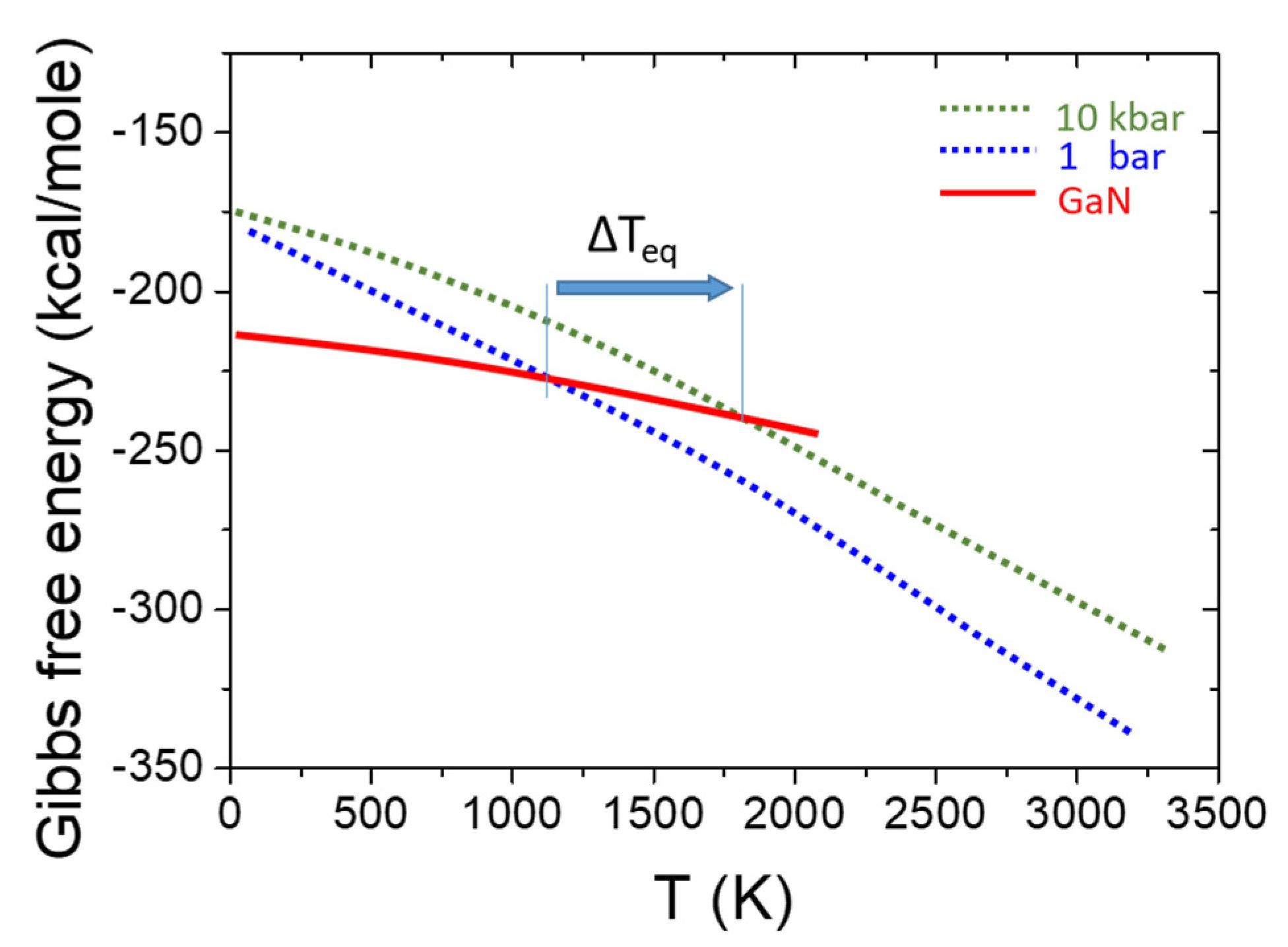
Figure 2.
Equilibrium N2 pressure over III-V nitrides. The dashed lines show the maximum pressure and temperature available in the gas pressure system of large volume. Adapted from Ref. [4].
Figure 2.
Equilibrium N2 pressure over III-V nitrides. The dashed lines show the maximum pressure and temperature available in the gas pressure system of large volume. Adapted from Ref. [4].
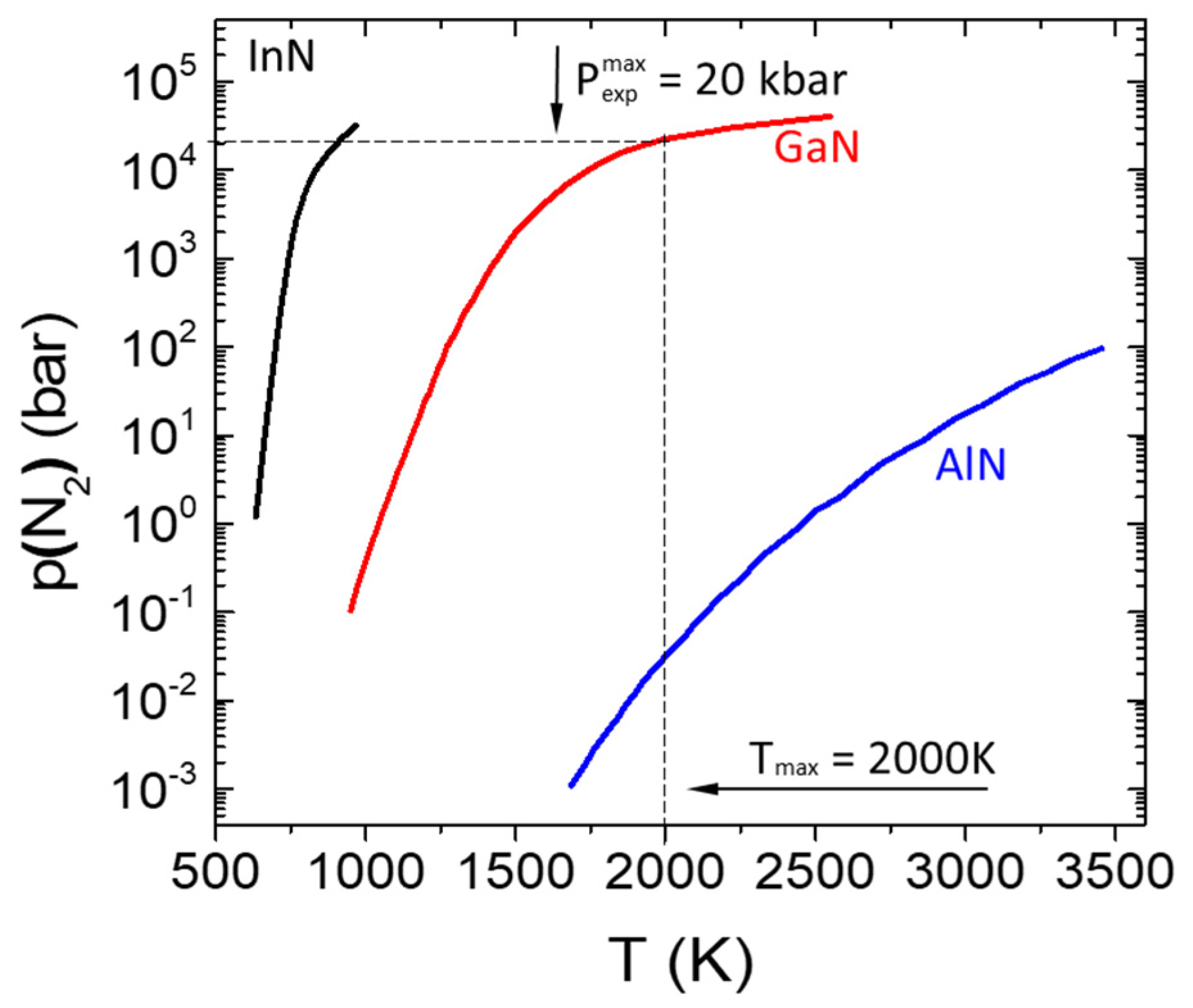
Figure 3.
Pressure coefficients of the direct gaps of various III-V compounds as a function of the ratio between their ionicity fi and lattice constant, a. Ionicity values are taken from Ref. [34].
Figure 3.
Pressure coefficients of the direct gaps of various III-V compounds as a function of the ratio between their ionicity fi and lattice constant, a. Ionicity values are taken from Ref. [34].
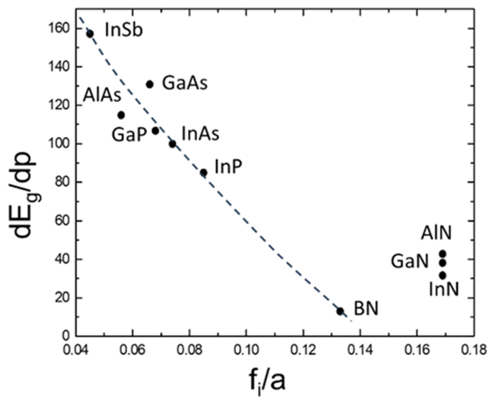
Figure 4.
Bulk modulus for typical III-V compounds and for nitrides as: (a) function of their lattice constant, and (b) their lattice constant to ionicity ratio.
Figure 4.
Bulk modulus for typical III-V compounds and for nitrides as: (a) function of their lattice constant, and (b) their lattice constant to ionicity ratio.
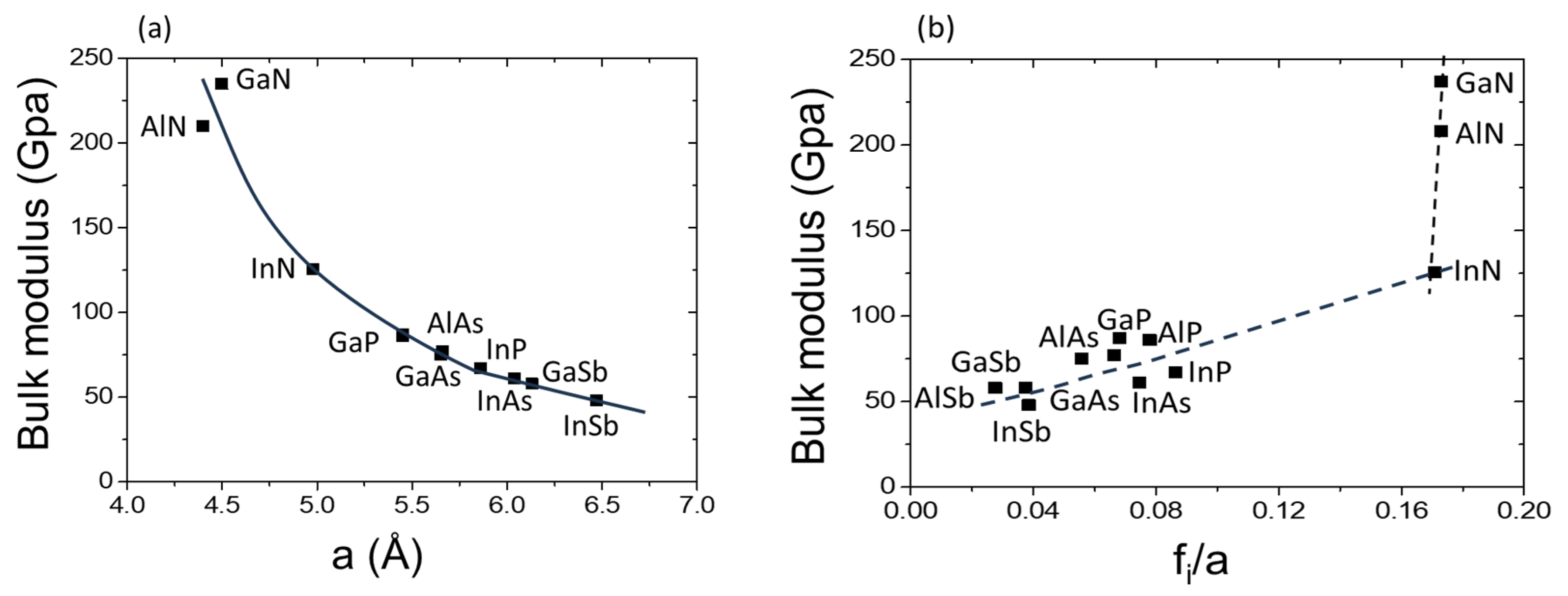
Figure 5.
Calculated total energies for (a) GaN and (b) AlN in wurtzite (wz) and rock salt (rs) structure as a function of volume relative to the equilibrium volume.
Figure 5.
Calculated total energies for (a) GaN and (b) AlN in wurtzite (wz) and rock salt (rs) structure as a function of volume relative to the equilibrium volume.
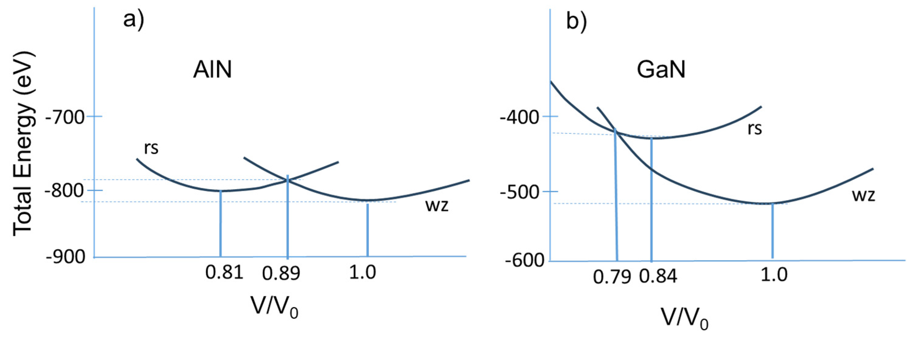
Figure 6.
The calculated effective mass of InN as a function of the electron concentration for two pressure values: 0 and 10 GPa. Based on Figure 6 and Figure 7a of Ref. [48].
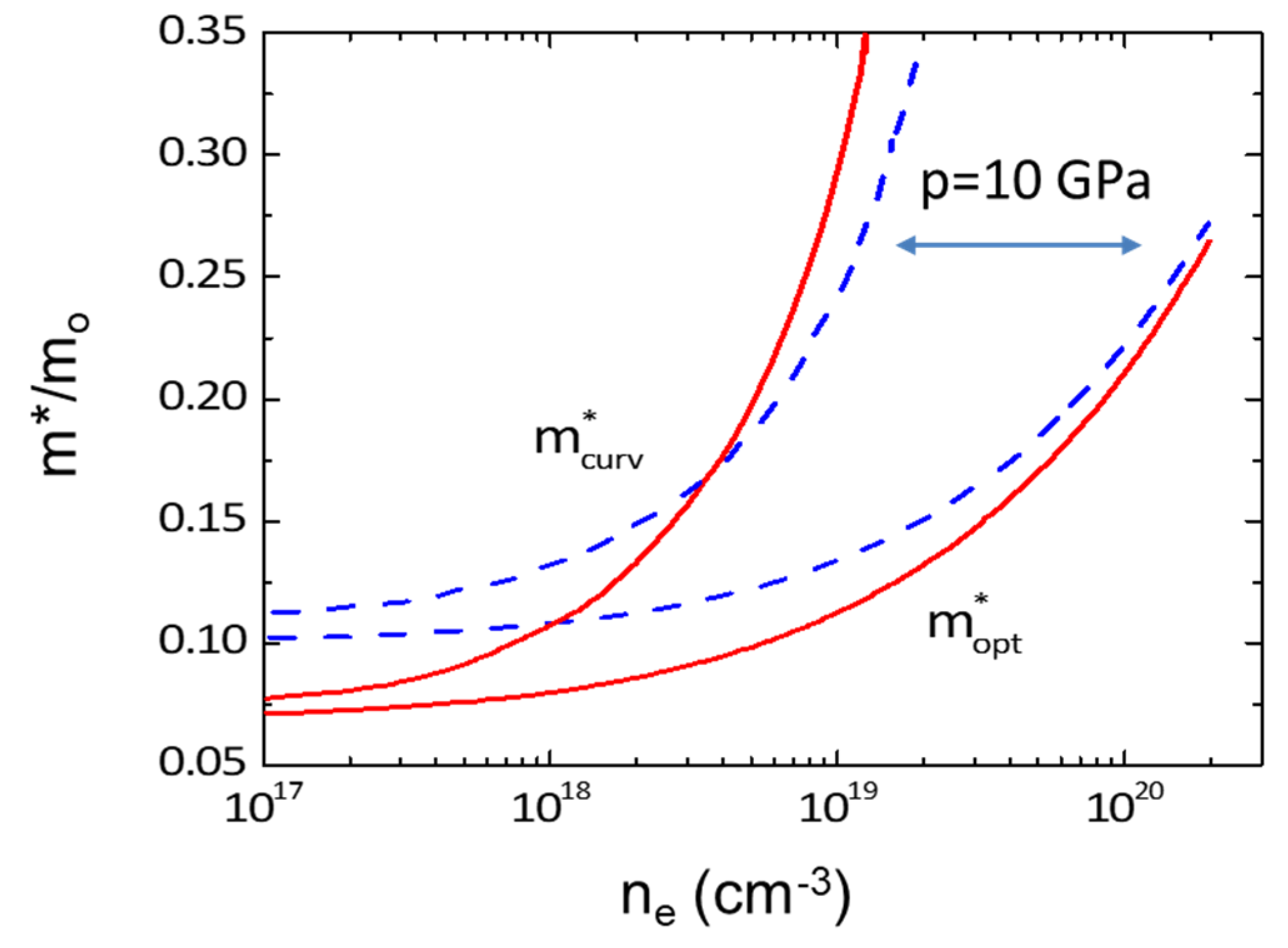
Figure 7.
Schematic representation of the effect of hydrostatic pressure on the optical band gap Eopt at high electron concentration. Black areas cover identical areas, as the number of electrons does not vary with pressure. Based on Figure 4 of Ref. [42].
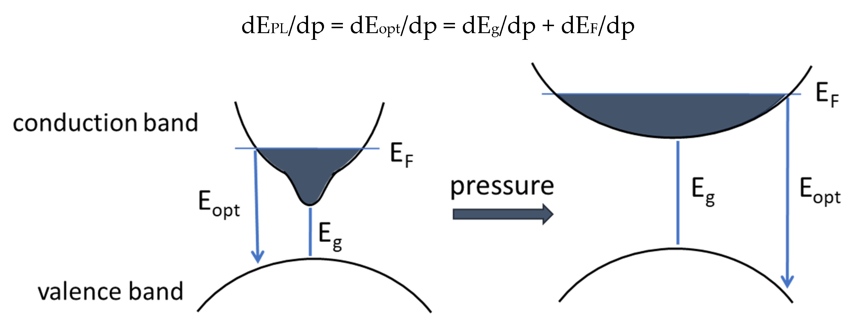
Figure 8.
dEg/dp as functions of x for InxGa1-xN and InxAl1-xN. Symbols represent the experimental values. Solid and dashed lines represent uniform and clustered arrangements of In atoms, respectively. The experimental data for InxGa1-xN are taken from Ref. [5] and for InxAl1-xN from Refs. [6,55].
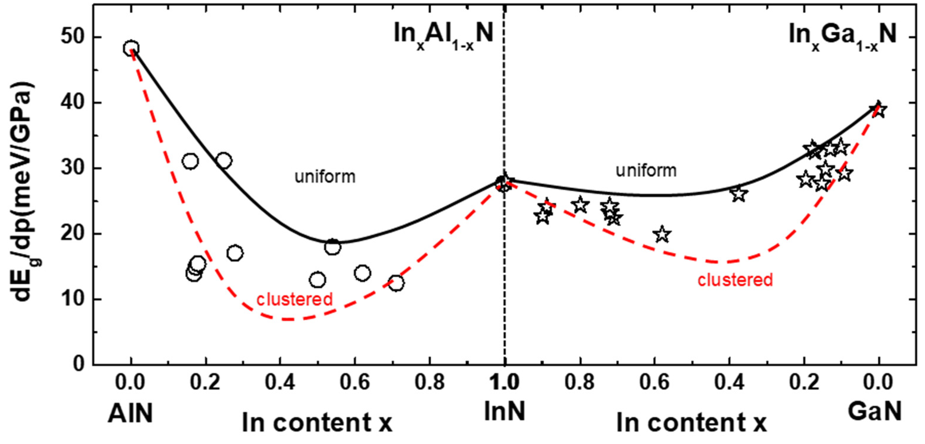
Figure 9.
Schematic illustration of the emergence of the resonant DX state of oxygen (high doping level) into the gap under pressure.
Figure 9.
Schematic illustration of the emergence of the resonant DX state of oxygen (high doping level) into the gap under pressure.
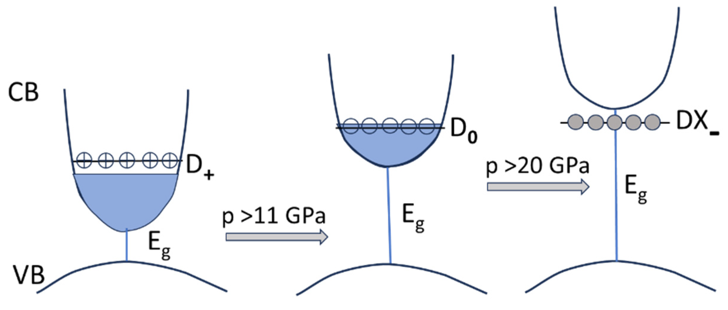
Figure 10.
Schematic configuration coordinate diagram for oxygen displacements in AlGaN. The diagram includes the optical ionization energy (Eopt), as well as the capture (Ec) and emission (Ee) barriers. Based on the calculations in Ref. [63].
Figure 10.
Schematic configuration coordinate diagram for oxygen displacements in AlGaN. The diagram includes the optical ionization energy (Eopt), as well as the capture (Ec) and emission (Ee) barriers. Based on the calculations in Ref. [63].
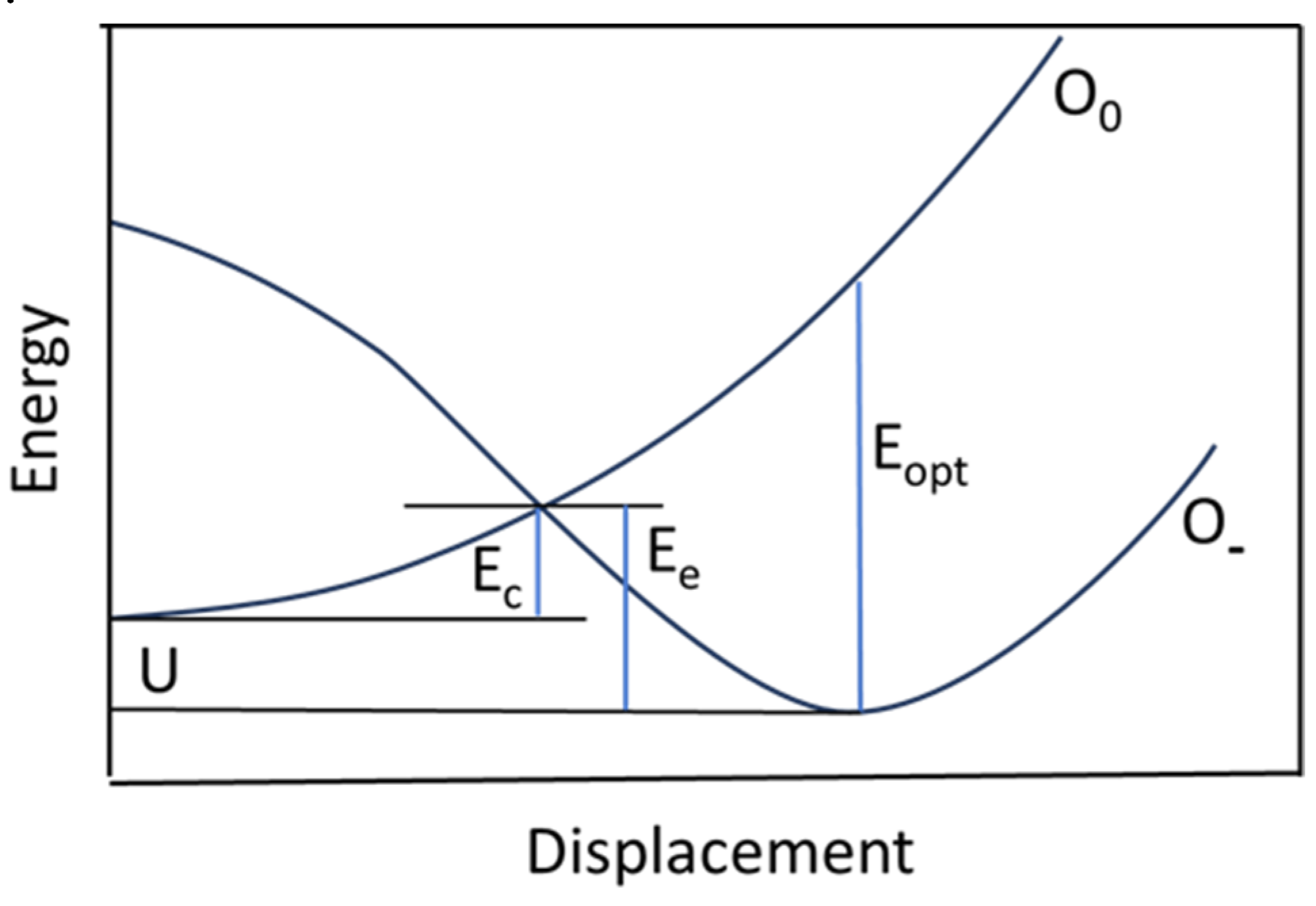
Figure 11.
Comparison of the band structure profiles along c-axis of wurtzite structure for single QW without (left) and with (right) built-in electric field. F denotes the built-in electric field. EL corresponds to the luminescence energy.
Figure 11.
Comparison of the band structure profiles along c-axis of wurtzite structure for single QW without (left) and with (right) built-in electric field. F denotes the built-in electric field. EL corresponds to the luminescence energy.
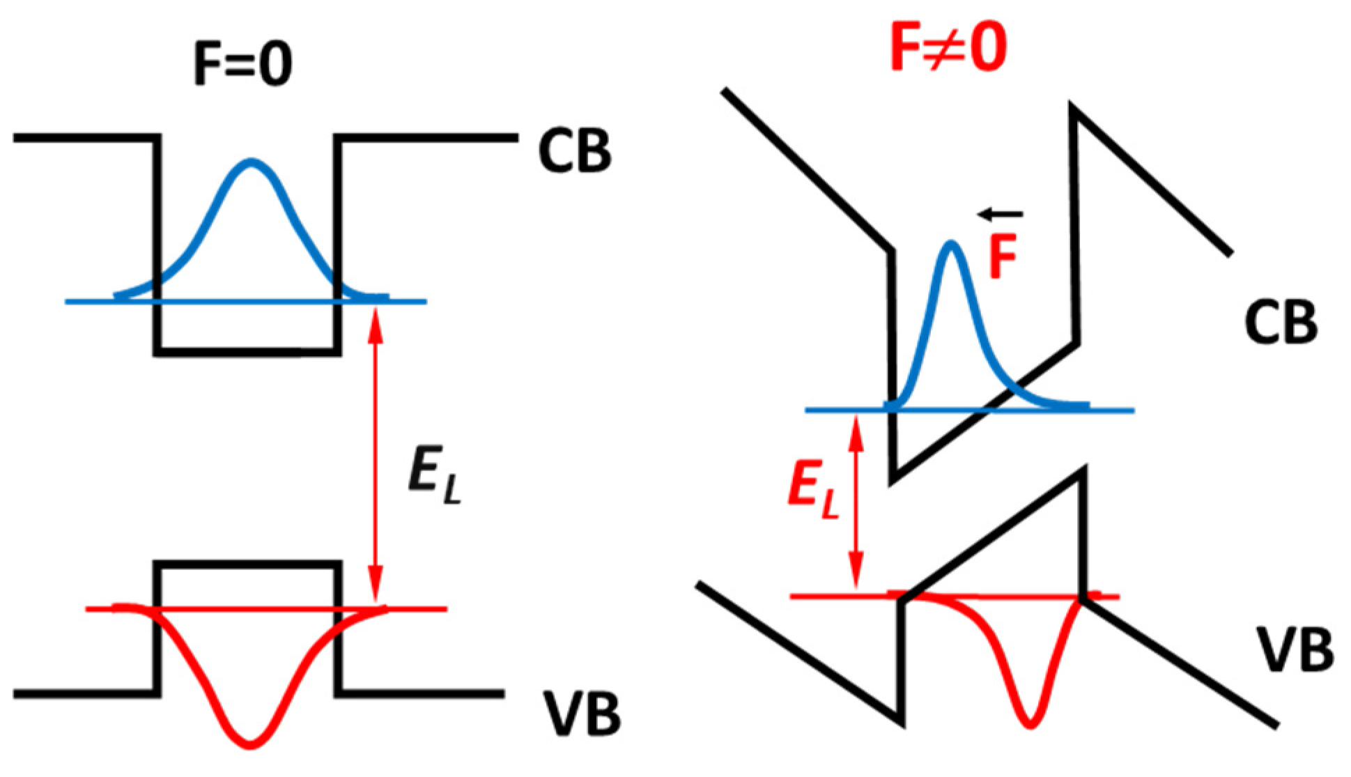
Figure 12.
(Color online). Schematic dependence of PL peak position on pressure in GaN/Al0.3Ga0.7N for different QW thicknesses. Two cases are illustrated: QWs grown along non-polar (dashed lines) and polar (solid lines) crystallographic directions. Based on Figure 13 of Ref. [70].
Figure 12.
(Color online). Schematic dependence of PL peak position on pressure in GaN/Al0.3Ga0.7N for different QW thicknesses. Two cases are illustrated: QWs grown along non-polar (dashed lines) and polar (solid lines) crystallographic directions. Based on Figure 13 of Ref. [70].
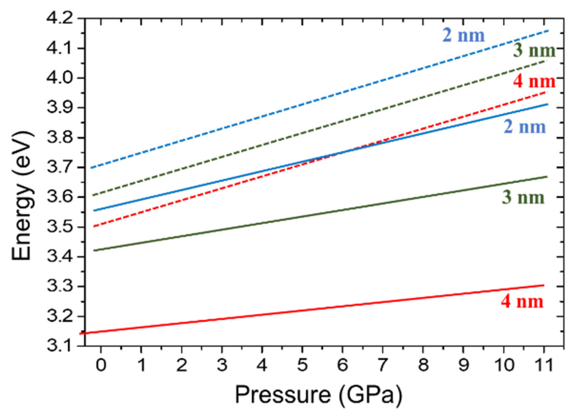
Figure 13.
Dependence of the dEPL/dp on the QW width for QWs in GaN/AlxGa1-xN with different Al concentrations, x (Refs. [76,77]).
Figure 13.
Dependence of the dEPL/dp on the QW width for QWs in GaN/AlxGa1-xN with different Al concentrations, x (Refs. [76,77]).
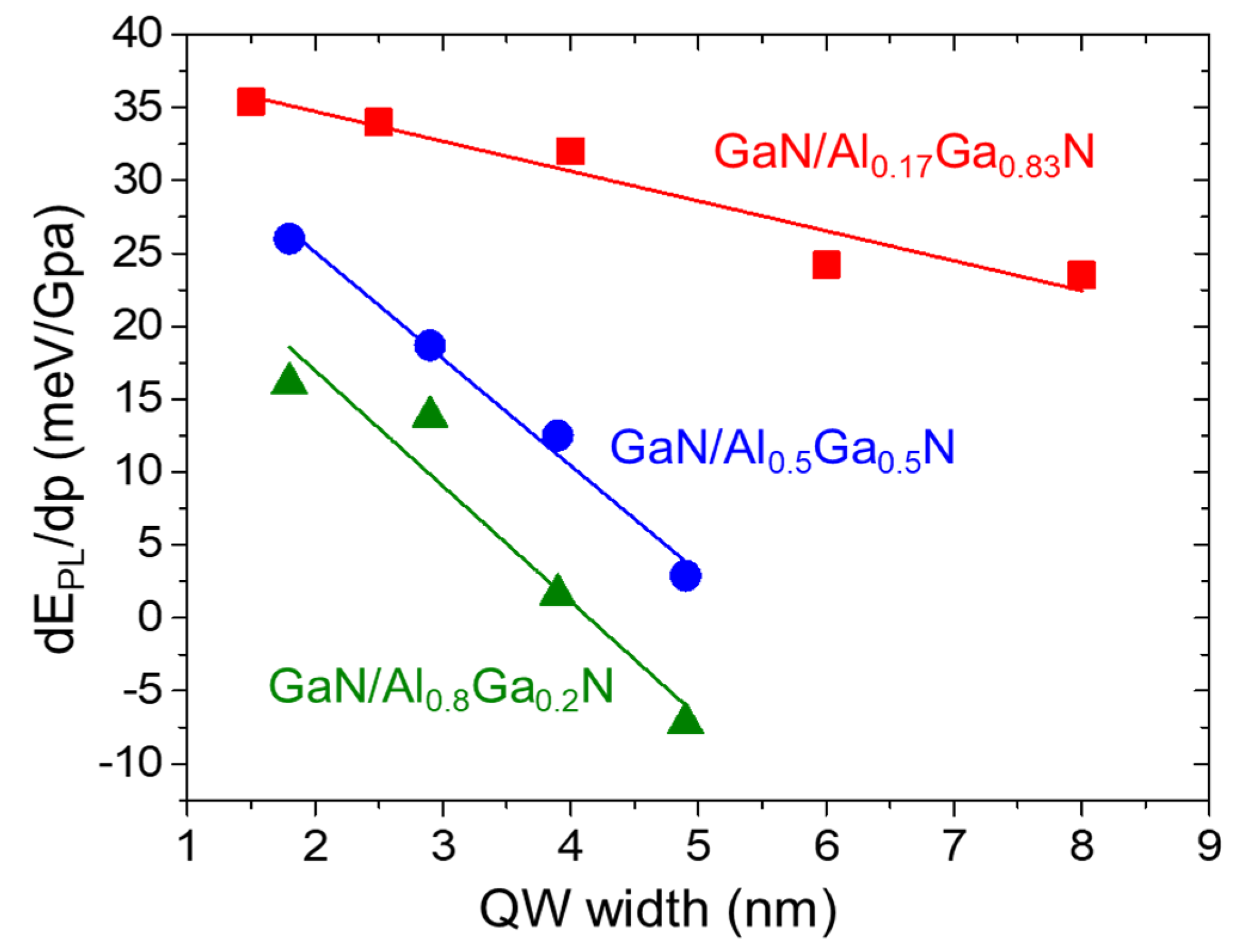
Figure 14.
Pressure dependencies of the PL peak energies of 3 samples (A,B,C) of GaN/Al0.88In0.12N QWs, measured at 10 K. The values of QW widths and the pressure coefficients for different samples are given in the plots. Based on Figure 11 of Ref. [70].
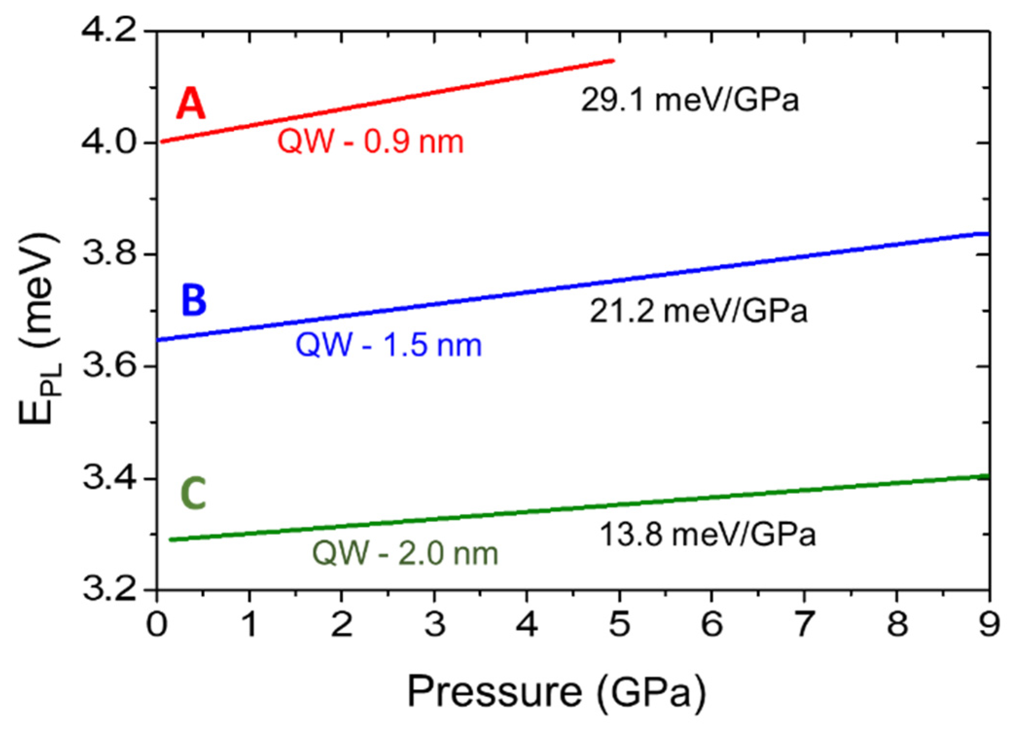
Figure 15.
PL pressure coefficients of wurtzite (Ref. [75]) and cubic (Ref. [110]) In0.20Ga0.80N/GaN QWs as a function of QW width.
Figure 15.
PL pressure coefficients of wurtzite (Ref. [75]) and cubic (Ref. [110]) In0.20Ga0.80N/GaN QWs as a function of QW width.
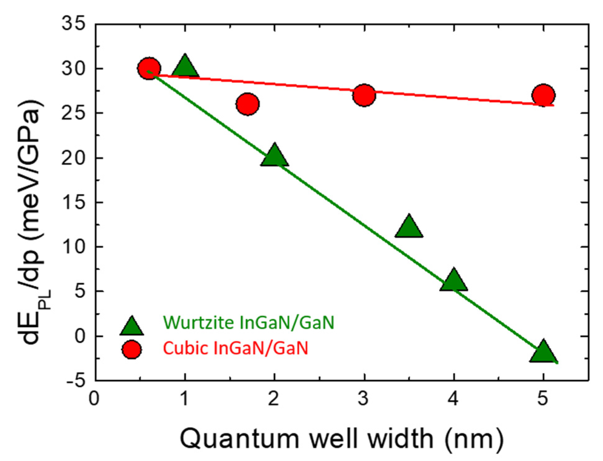
Figure 16.
Comparison of the dEPL/dp for InGaN alloy and for InGaN/GaN QWs for different QW widths (as described in the Figure). Experimental data are from Ref. [5] (for InGaN alloy) and Ref. [75] (for InGaN/GaN QWs). The polynomial fit to the theoretical dEg/dp values for InGaN alloy is shown by the solid line.
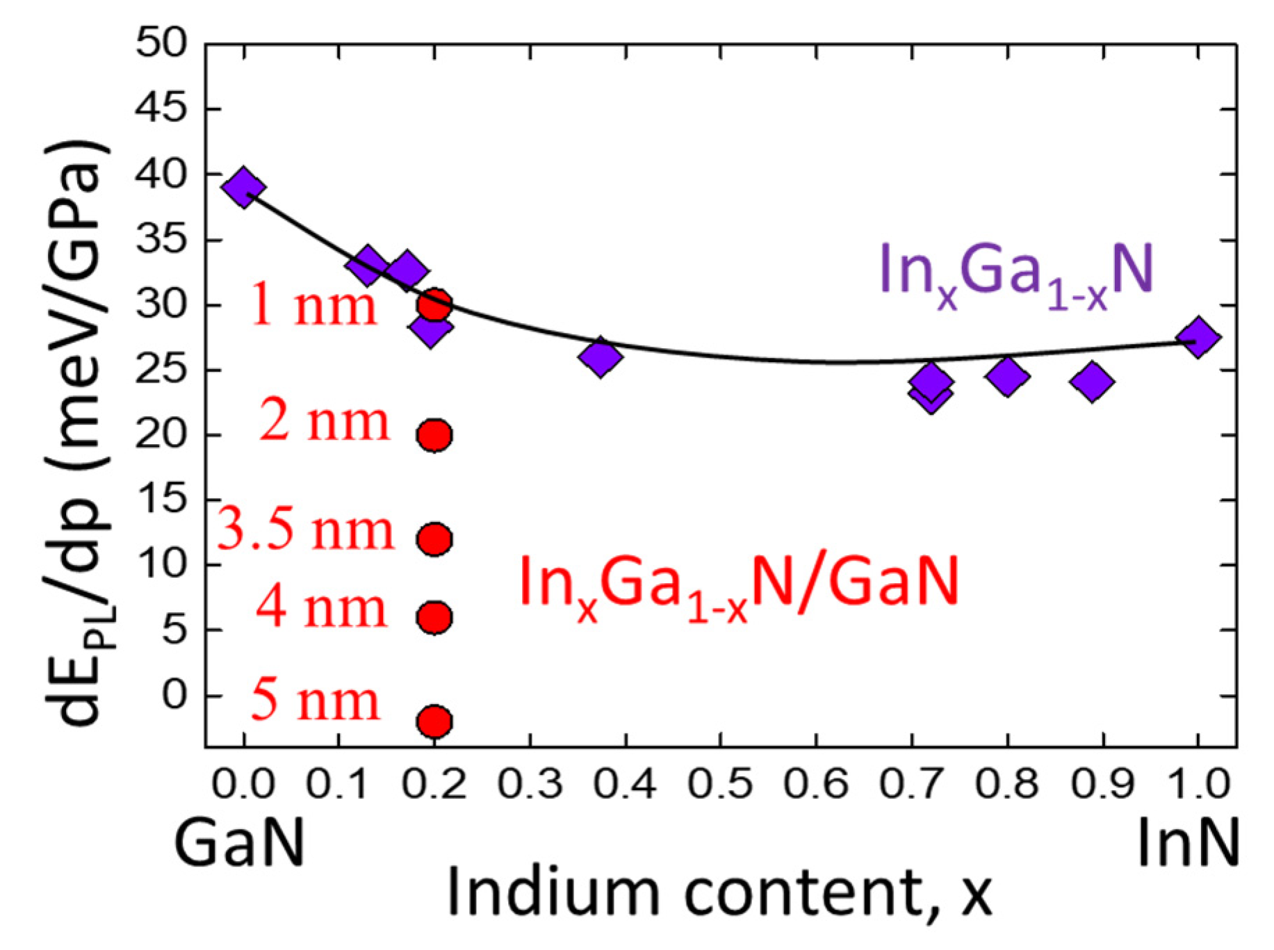
Figure 17.
Calculated pressure coefficients of the band gaps (diamonds) of 1InxGa1-xN/nGaN SLs and 1InN/nGaN SLs compared with experimental data (circles). Values of n are given. The lines are spline fits to guide the eye. Reproduced with permission from Ref. [116] (Figure 27). Copyright 2018 IOP Publishing CC BY licence.
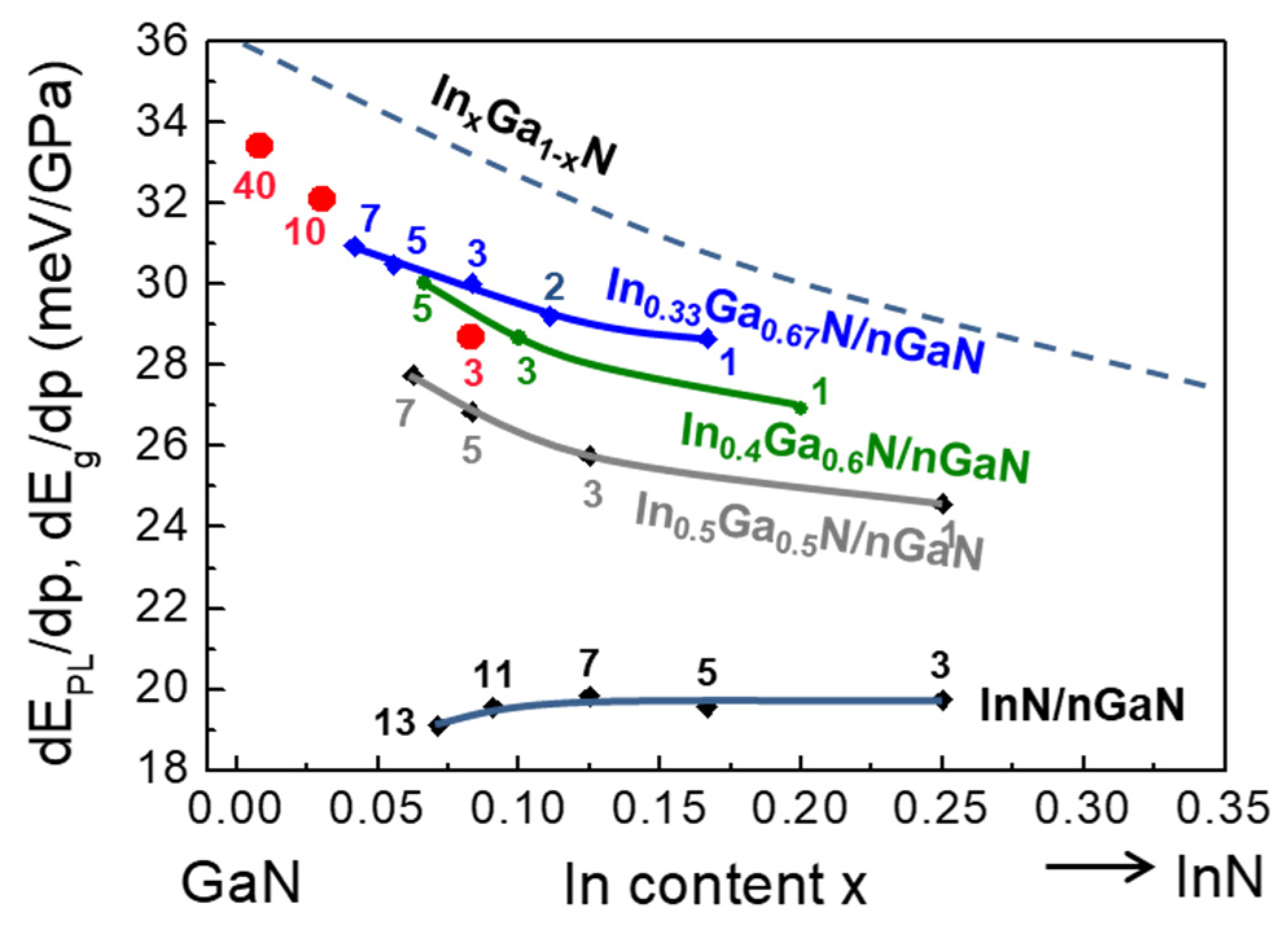
Figure 18.
Schematic structures of: a) LED with tunnel junction above the QW, b) LD structure with AlGaN cladding to form the waveguide. In both structures the active layer consists of In0.17Ga0.83N QW.
Figure 18.
Schematic structures of: a) LED with tunnel junction above the QW, b) LD structure with AlGaN cladding to form the waveguide. In both structures the active layer consists of In0.17Ga0.83N QW.
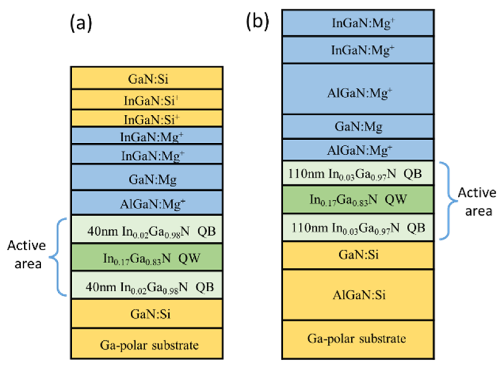
Figure 19.
a) EL spectra for LED1, LED2, and LED3 measured at the different driving currents, (b) EL energy vs. current density for the studied LEDs.
Figure 19.
a) EL spectra for LED1, LED2, and LED3 measured at the different driving currents, (b) EL energy vs. current density for the studied LEDs.
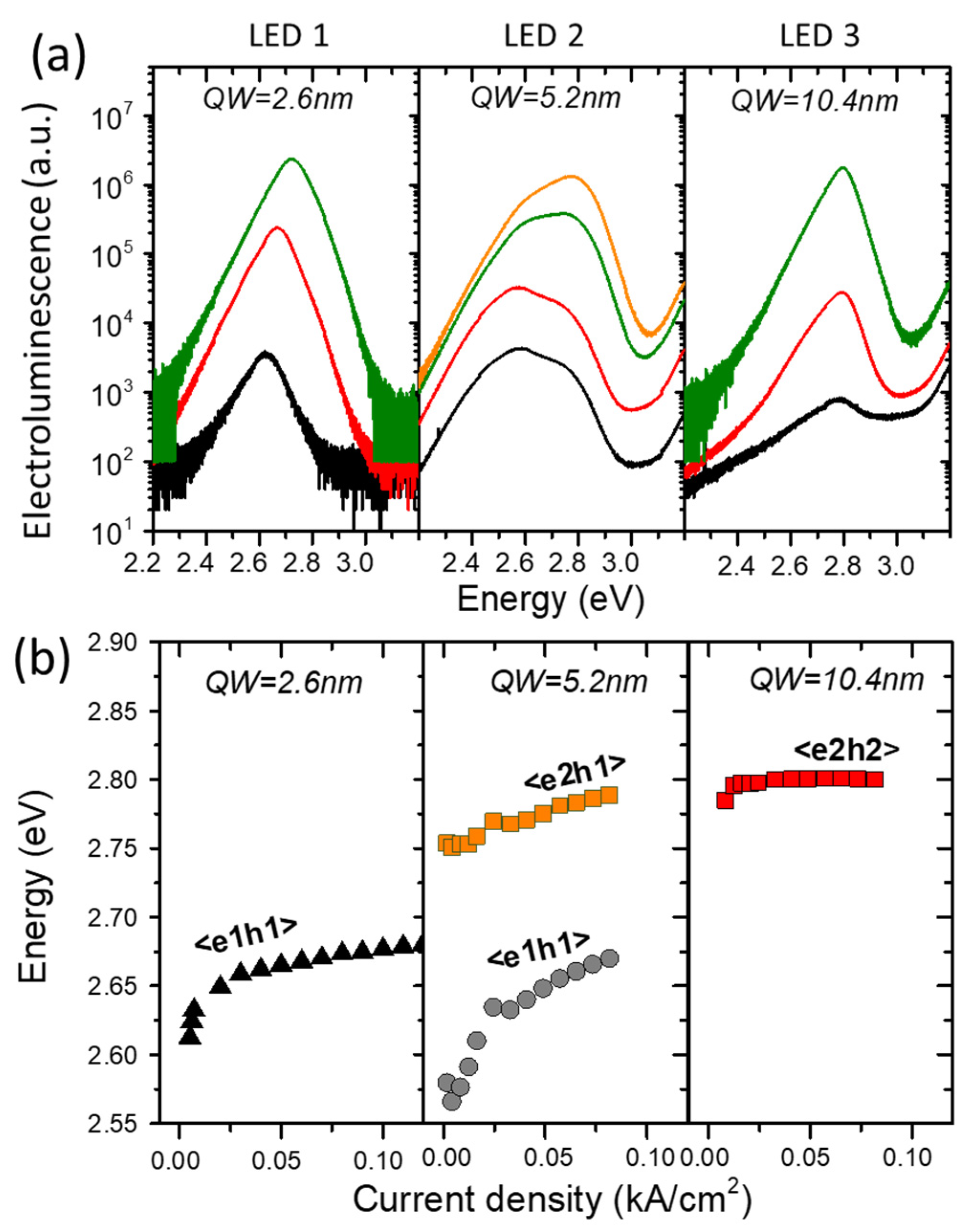
Figure 20.
a) Normalized EL spectra measured in LED3 for 3 selected values of the applied hydrostatic pressure: 0.1GPa, 0.5GPa and 1 GPa. b) Pressure dependence of the maxima of the EL spectra for the pressure range: 0.1-1.0 GPa.
Figure 20.
a) Normalized EL spectra measured in LED3 for 3 selected values of the applied hydrostatic pressure: 0.1GPa, 0.5GPa and 1 GPa. b) Pressure dependence of the maxima of the EL spectra for the pressure range: 0.1-1.0 GPa.
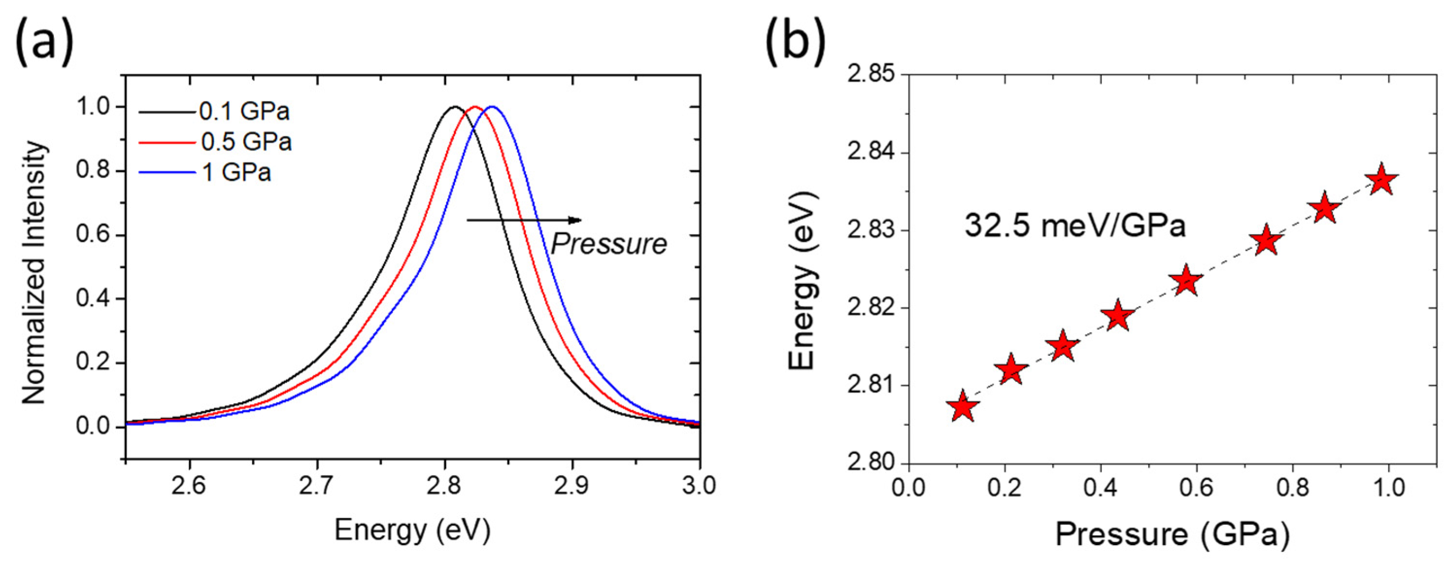
Figure 21.
Pressure coefficient of the EL emission energy vs. driving current density, ID in the studied LEDs. Energetic states of electrons and holes involved in radiative recombination are shown.
Figure 21.
Pressure coefficient of the EL emission energy vs. driving current density, ID in the studied LEDs. Energetic states of electrons and holes involved in radiative recombination are shown.
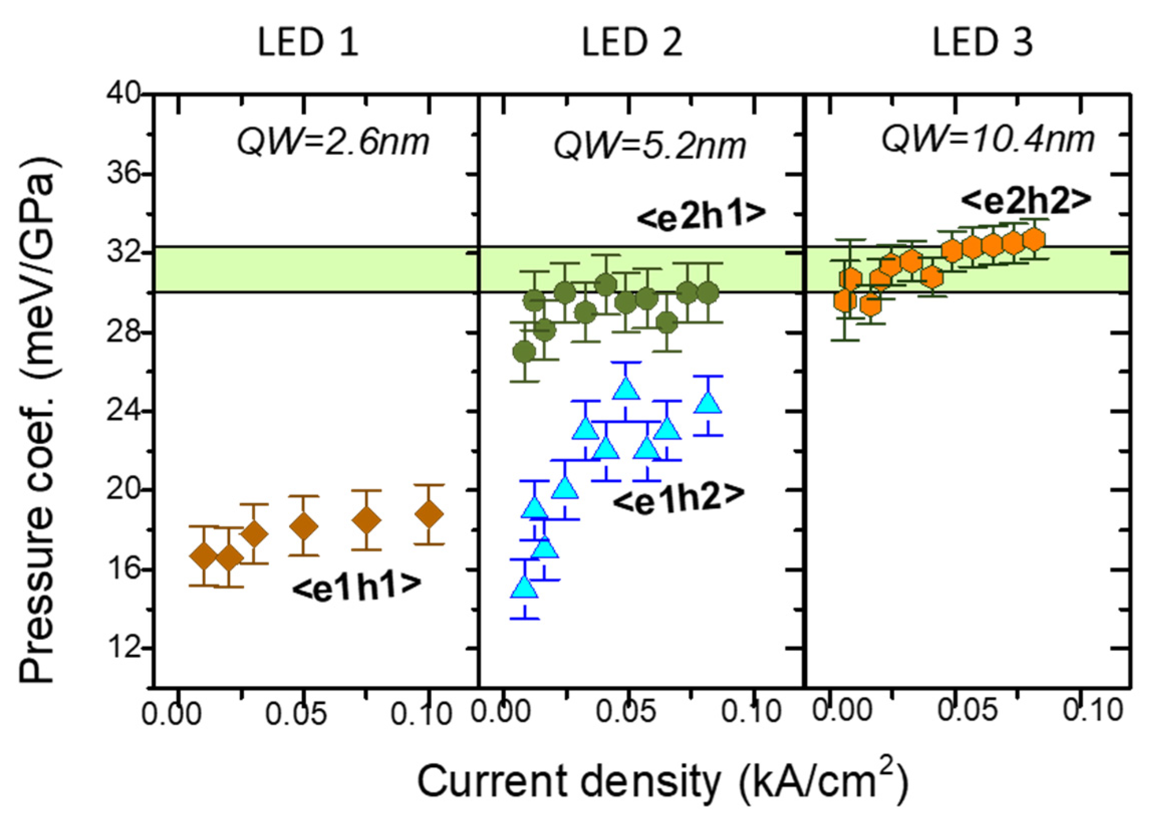
Figure 22.
Current density dependence of pressure coefficients for two LDs with QWs of different widths: a) 2.6 nm and b) 10.4 nm. The light green horizontal bars represent the pressure coefficient value corresponding to a fully screened built-in field. The violet bars represent the driving current range above the laser threshold.
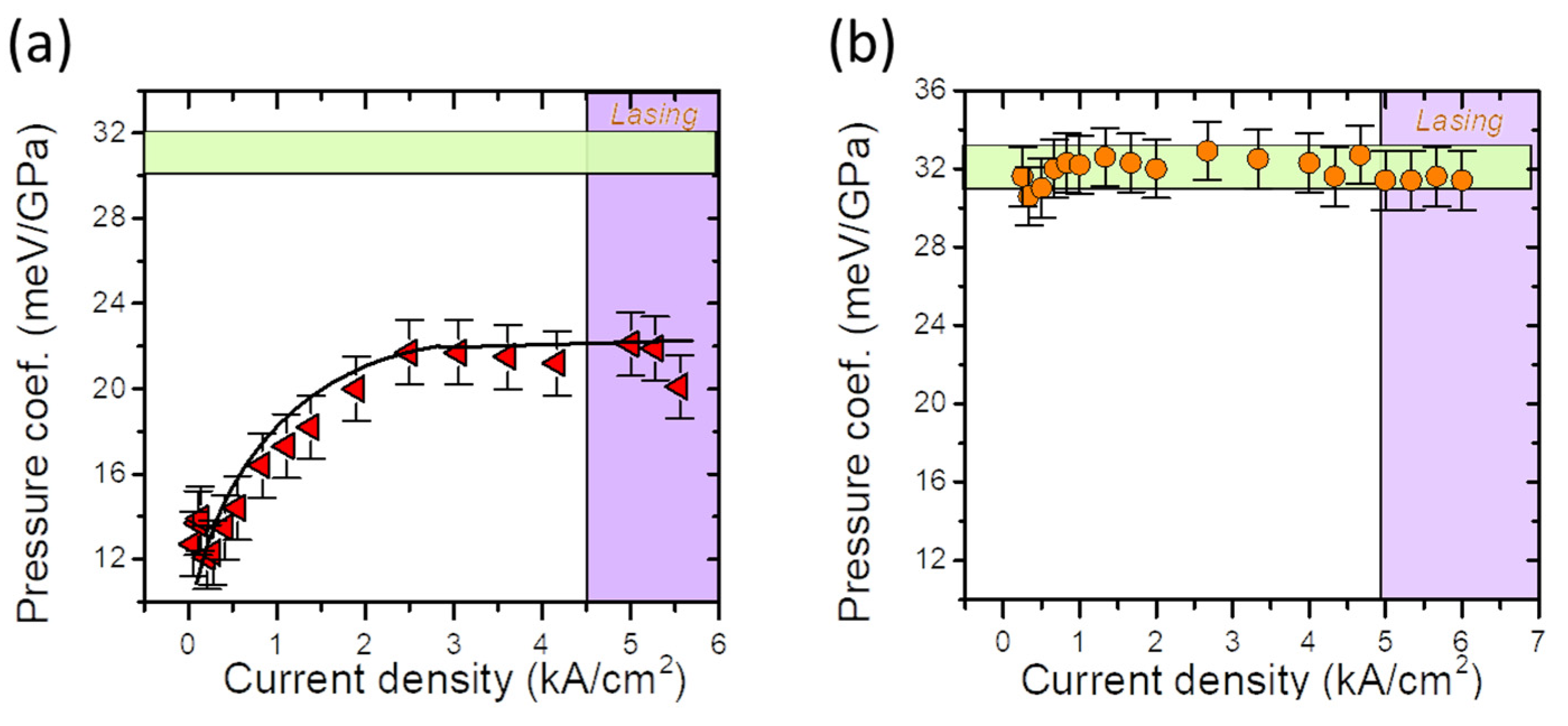

Table 1.
Basic parameters of nitrides; the band gaps, Eg, pressure coefficient, dEg/dp, the effective lattice constants, aeff, and ionicities fi.
Table 1.
Basic parameters of nitrides; the band gaps, Eg, pressure coefficient, dEg/dp, the effective lattice constants, aeff, and ionicities fi.
| InN | GaN | AlN | |
|---|---|---|---|
| Eg (eV) | 0.7-0.8a, 0.76b, 0.61c | 3.47d | 6.04e |
| dEg/dp (meV/GPa) | 27.4f, 29+-1g | 41.4h | 49e |
| Lattice constant, aeff (Å) | 4.98 | 4.50 | 4.37 |
| Ionicity Ref. [34] | 0.859 | 0.770 | 0.775 |
| Ionicity Ref. [35] | 0.578 | 0.500 | 0.449 |
| Ionicity Ref. [36] | 0.853 | 0.778 | 0.794 |
Table 2.
Experimental values of bulk modulus, B, and phase transition pressure, PT, for the nitrides considered.
Table 2.
Experimental values of bulk modulus, B, and phase transition pressure, PT, for the nitrides considered.
| InN Ref. [46] | GaN Ref. [46] | AlN Ref. [46] | |
|---|---|---|---|
| B (GPa) | 125.5 | 237 | 207.9 |
| PT (GPa) | 12.1 | 52.2 | 22.9 |
Table 3.
Experimental values of InN, GaN and AlN electron effective masses m* (in units of the free-electron mass).
Table 3.
Experimental values of InN, GaN and AlN electron effective masses m* (in units of the free-electron mass).
| InN | GaN | AlN | |
|---|---|---|---|
| m* | 0.05b, 0.07c, 0.044d | 0.20e 0.18-0.29f |
0.40e 0.29-0.45f |
| dm*/dp | 0.04/GPa a | ||
| dlnm*/dlnV | 1.1-1.2f | 1.7-1.8f |
Disclaimer/Publisher’s Note: The statements, opinions and data contained in all publications are solely those of the individual author(s) and contributor(s) and not of MDPI and/or the editor(s). MDPI and/or the editor(s) disclaim responsibility for any injury to people or property resulting from any ideas, methods, instructions or products referred to in the content. |
© 2024 by the authors. Licensee MDPI, Basel, Switzerland. This article is an open access article distributed under the terms and conditions of the Creative Commons Attribution (CC BY) license (http://creativecommons.org/licenses/by/4.0/).
Copyright: This open access article is published under a Creative Commons CC BY 4.0 license, which permit the free download, distribution, and reuse, provided that the author and preprint are cited in any reuse.


