Preprint
Article

Experimental and Theoretical Analysis of Rayleigh and Leaky-Sezawa Waves Propagating in ZnO/Fused Silica Substrates

Altmetrics

Downloads

98

Views

29

Comments

0

A peer-reviewed article of this preprint also exists.

Submitted:

25 June 2024

Posted:

26 June 2024

You are already at the latest version

Alerts
Abstract
Piezoelectric c-axis oriented zinc oxide (ZnO) thin films, from 1.8 up to 6.6 µm thick, have been grown by radio frequency magnetron sputtering technique onto fused silica substrates. A delay line consisting in two interdigital transducers (IDTs) with wavelength λ = 80 µm was photolith-ographically implemented onto the surface of the ZnO layers. Due to the IDTs split finger con-figuration and metallization ratio (0.5), the propagation of both the fundamental, third and nineth harmonic Rayleigh waves is excited; also, three leaky surface acoustic waves (SAWs) were detected travelling at velocity close to that of the longitudinal bulk wave in SiO2. The acoustic waves propagation in ZnO/fused silica was simulated by using 2D finite-element method (FEM) tech-nique to identify the nature of the experimentally detected waves. It turned out that, in addition to the fundamental and harmonic Rayleigh waves, also high-frequency leaky surface waves are ex-cited by the harmonic wavelengths; such modes are identified as leaky-Sezawa (LS) waves under cut-off. The velocity of all the modes was found in good agreement with the theoretically calcu-lated values. The existence of a low-loss region for the Sezawa wave below the cut off was theo-retically predicted and experimentally assessed.
Keywords: 
Subject: Physical Sciences  -   Acoustics

1. Introduction

Rayleigh waves are surface acoustic waves (SAWs) that travel along the surface of elastic half-spaces. If the propagating medium is piezoelectric, the SAW propagation can be excited by electrical means and is characterized by both mechanical displacement components and an electrical potential wave, predominantly concentrated up to about one wavelength in depth from the propagating medium surface. When the propagating medium consists in a piezoelectric film/substrate heterostructure, multiple Rayleigh modes can propagate [1,2] if the velocity of the transverse bulk acoustic wave (BAW) in the substrate is higher than that in the overlayer. This heterostructure is name slow on fast structure and the ZnO/fused silica combination is a typical example since the shear BAW velocity in fused silica and ZnO is equal to 3766 and 2829 m/s, respectively. All the high-order modes except the fundamental wave have a cut off frequency: above the cut off, the velocity of the modes is higher than the transverse BAW velocity in the substrate and thus they leak energy in the substrate; below the cut off, the velocity of the modes decreases steadily with frequency and tends to the shear velocity of the BAW in the layer material. As a result, the leaky region above the cut off is characterized by a non-zero attenuation, as opposed to the high-frequency region where the waves travel poorly attenuated. In the available scientific literature [3,4,5,6,7] the propagation of leaky Sezawa waves has been observed experimentally and predicted theoretically in structures consisting of a highly anisotropic fast half-space (such as 4H-SiC, diamond and sapphire) covered by a thin epitaxial piezoelectric layer (such as GaN, ScAlN or AlN). Like GaN, AlN and ScAlN, zinc oxide is also a piezoelectric material which can be grown in the form of a highly oriented thin film; its SAW velocity is slower than that of the formers, but it has the largest electromechanical coupling coefficient K2 among them. Since the leaky Sezawa modes maintain the K2 of the piezoelectric overlayer, the use of a low-cost substrate (such as fused silica) and a ZnO layer represents a remarkable advantage in view of reducing the fabrication costs while ensuring high performances.
This paper reports numerical simulations and experimental results on the generation of Rayleigh and leaky-Sezawa waves in low-cost ZnO/fused silica substrates. A delay line consisting in two split fingers interdigital transducers (IDTs) with metallization ratio of 0.5 and wavelength λ = 80 µm was photolithographically implemented onto the surface of the ZnO layer. The propagation of fundamental and even harmonic Rayleigh waves is excited in the ZnO/SiO2 substrate in the ~37 to ~300 MHz frequency range, namely the fundamental, third, and nineth harmonic SAWs, for ZnO layer thickness ranging from 1.8 up to 6.6 µm. Leaky SAWs were also detected in the ~72 to ~500 MHz frequency range. The SAWs propagation in ZnO/SiO2 was simulated using two-dimensional (2D) finite-element method (FEM) technique (by the commercial software COMSOL Multiphysics 6.1) to identify the nature of the experimentally detected waves. It turned out that, in addition to the fundamental and harmonic Rayleigh waves, also leaky surface waves are excited by the harmonic wavelengths: such high-frequency modes are identified as leaky Sezawa (LS) waves under cut-off. The FEM analysis was performed to study the modes characteristics (modes shape, velocity, electroacoustic coupling efficiency K2 and propagation loss) and to assign each experimentally observed frequency the proper SAW mode. The experimental data were found in good agreement with the theoretically predicted values. The existence of a low-loss region for the Sezawa wave below the cut off was theoretically predicted and experimentally assessed.
Exploiting split-finger IDTs, which operate highly efficiently at the third harmonic wave, to excite high-velocity LS modes in ZnO/SiO2 substrates, allows us to achieve an improved resonant frequency by using electrodes with finger- and inter-finger spacing easily achievable with inexpensive conventional photolithographic techniques [8].
The LS modes are worth of investigation because of their velocities larger than the Rayleigh velocity in the substrate which leads to enhanced operation frequency of the SAW devices without requiring expensive nanofabrication techniques necessary to reduce the metal electrode dimensions.

2. Materials and Methods

2.1. SAW Propagation in Layered Media

Surface acoustic waves can travel along the surface of an elastic half-space with a phase velocity which depends on the crystallographic cut of the propagating medium and on the propagation direction. In single-material half-space, the confinement mechanism of the SAWs depends on the presence of a stress-free surface. The propagation of the SAWs along the surface of a piezoelectric medium is excited and detected by metal interdigitated transducers (IDTs) which consists of spatially periodic thin-film metal electrodes placed in contact with the medium surface; the fingers periodicity represents the wavelength λ of the travelling acoustic mode. By applying an alternating voltage to the launching IDT, a periodic electric field is imposed on the piezoelectric substrate’s surface and a SAW is produced because of the generation of a periodic strain field. The generated SAW travels through a certain distance (the wave path) and reaches the output IDT which detects the electric voltage associated with the SAW. The IDTs parameters (such as the IDT finger width and spacing, fingers overlapping, number of finger pairs) affect the IDTs performance; the double electrode split IDT structure minimizes internal reflections (it is called non-reflective transducers because the internal reflection phenomenon is shifted at the double of the centre frequency) that otherwise complicate the IDT response [9,10,11,12]. The ability of the split IDT to generate harmonics of the fundamental mode strongly depends on the metallization ratio of the fingers [13,14]: for 0.5 metallization ratio, the split finger IDT allows highly efficiency at the third harmonic and hence high working frequency ranges which would otherwise require expensive lithographic techniques; the 5th and 7th harmonics are suppressed as the resulting wave would have the same piezoelectric potential at all IDT fingers, meaning that no electrical energy can be transferred in the respective surface wave mode by applying a voltage between the IDT electrodes.
If the propagating medium consists of a layer/substrate structure, it can sustain the propagation of multiple SAWs: the first mode is called Rayleigh wave while the higher order modes are called Sezawa, R3, R4, and so on [1]. The condition required for this to happen is that the velocity of the transverse BAW of the half-space material is larger than that of the layer material. The number of SAW modes and their velocities depend on the layer thickness, h: for very thin film thickness (h/λ << 1), only the fundamental Rayleigh mode propagates with a velocity close to the SAW velocity of the substrate material (about 3450 m/s for fused quartz); by increasing the layer thickness (h/λ >> 1), the Rayleigh velocity asymptotically reaches the SAW velocity of the layer material (2644 m/s for c-ZnO). The velocity of higher order modes asymptotically reaches the velocity of BAW shear in the layer material as the layer thickness increases. The amplitude profile of the Rayleigh wave is predominantly confined in the layer and decays exponentially with the depth, while that of the higher order modes has an exponential tail in the substrate. The latter modes have a layer thickness-to-wavelength cut-off at which the phase velocity is equal to the substrate shear BAW velocity. Right at the cut-off, the SAW mode couples with bulk modes and shows a leaky nature, as the acoustic power flows into the bulk substrate, thus resulting in a large insertion loss.

2.2. FEM Analysis

The propagation of SAWs along ZnO/SiO2 structure was investigated by using 2D FEM analysis since the acoustic field was unchanged along the transverse direction, due to the crystallographic symmetry of the c-ZnO and the isotropy of the fused silica substrate. Comsol Multiphysics 6.1 software was used in the eigenfrequency and frequency domain studies. The models use a piezoelectric multiphysics coupling node with solid mechanics and electrostatic interfaces. The unit cell (width λ = 80 µm) consists in the following domains, as shown in Figure 1a: Air (2·λ thick), ZnO (from 1 to 80 µm thick), SiO2 (5·λ thick) and PML (2·λ thick). Four Al electrodes (0.15 µm thick and λ/8 wide) were placed onto the surface of the ZnO layer to perform the frequency domain study, as shown in Figure 1b: two neighbors electrodes were connected to a fixed electric potential (terminal type: voltage, 1 V) and the other two were grounded. Periodic boundary conditions ( l e f t a n d   r i g h t ) are applied to the lateral sides of the unit cell. The bottom boundary is fixed ( b o t t o m ), while electrically free or shorted boundary condition on the ZnO free surface ( i n t e r f a c e ) is used to calculate the electromechanical coupling coefficient (as explained later).
The material constants were extracted from the material library of COMSOL. The ZnO has 0.01 permittivity loss and 0.002 mechanical loss; SiO2 has isotropic mechanical loss equal to 0.01. An extremely fine mesh (i.e., maximum automatically generated physics-defined triangular elements) was chosen for all the FEM simulations to get more accurate results.
Eigenfrequency and frequency domain studies were performed to identify the type of the acoustic modes experimentally detected based on a comparison of the experimental data with numerical calculations. Figure 2 a-c shows, as an example, the solid displacement, the longitudinal and shear displacement components (u and v) of the LS wave for a ZnO layer 4 µm thick.
The fundamental and harmonic Rayleigh waves have elliptical polarization and travel along the surface of the propagating medium, up to a depth of about 1.5·λ from the surface. The LS waves are mostly longitudinally polarized, and their vertical displacement component increases while approaching the cut off. The LS waves leak energy from the layer into the substrate and becomes evanescent, thus exhibiting their leaky nature as demonstrated by the substantial vertical displacement component penetrating into the SiO2 substrate.
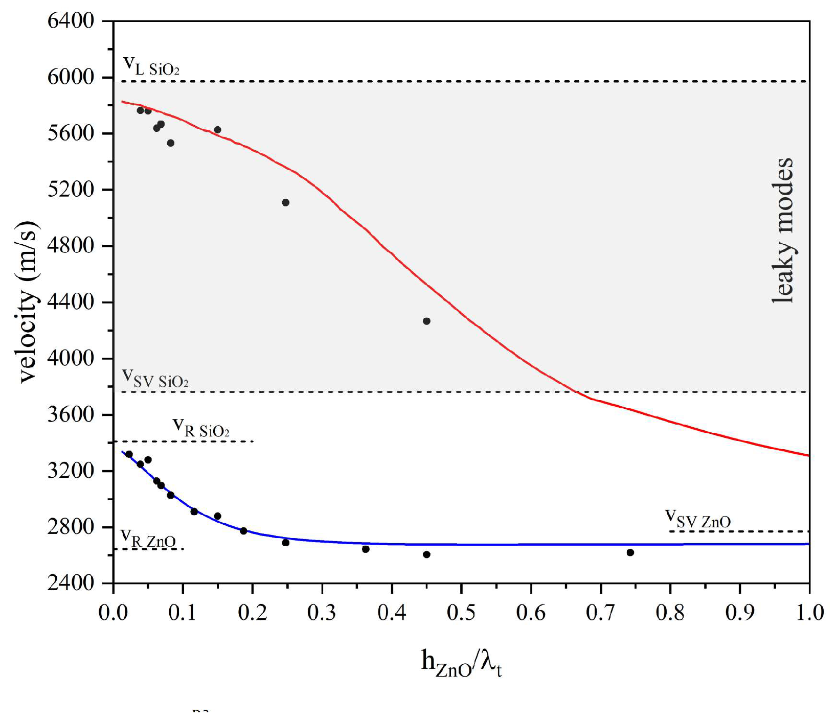
The phase velocity of the SAWs were calculated for different ZnO layer thicknesses and fixed wavelength (λ = 80 µm) by performing the sweep parameter eigenfrequency study: the modes velocity was calculated as v = λf, being λ = 80 µm the wavelength and f the eigenfrequency solution. Figure 3 shows the Rayleigh and Sezawa dispersion curves; the black points are the experimentally measured data which will be discussed in the next paragraphs.
For very thin film thicknesses, only the Rayleigh mode propagates; the Sezawa mode appears as it exceeds its cut-off value ( h λ c u t   o f f = 0.68). With further increases in h/λ (not shown in Figure 3), several unattenuated higher order Rayleigh modes appear at a succession of values of h λ c u t   o f f . Above the transverse BAW velocity of the substrate, no modes are allowed to propagate unattenuated: by assuming non-zero dielectric loss and mechanical damping, the velocity dispersion curves of the Sezawa and higher order mode extend between the transverse and longitudinal BAW velocity in the substrate where they become leaky modes, broadened through coupling to the bulk modes of the substrate, into which they radiate. At small h/λ, the LS velocity is close to that of the longitudinal BAW in SiO2 while in the high h/λ limit it tends to the velocity of the shear vertical BAW in the ZnO.
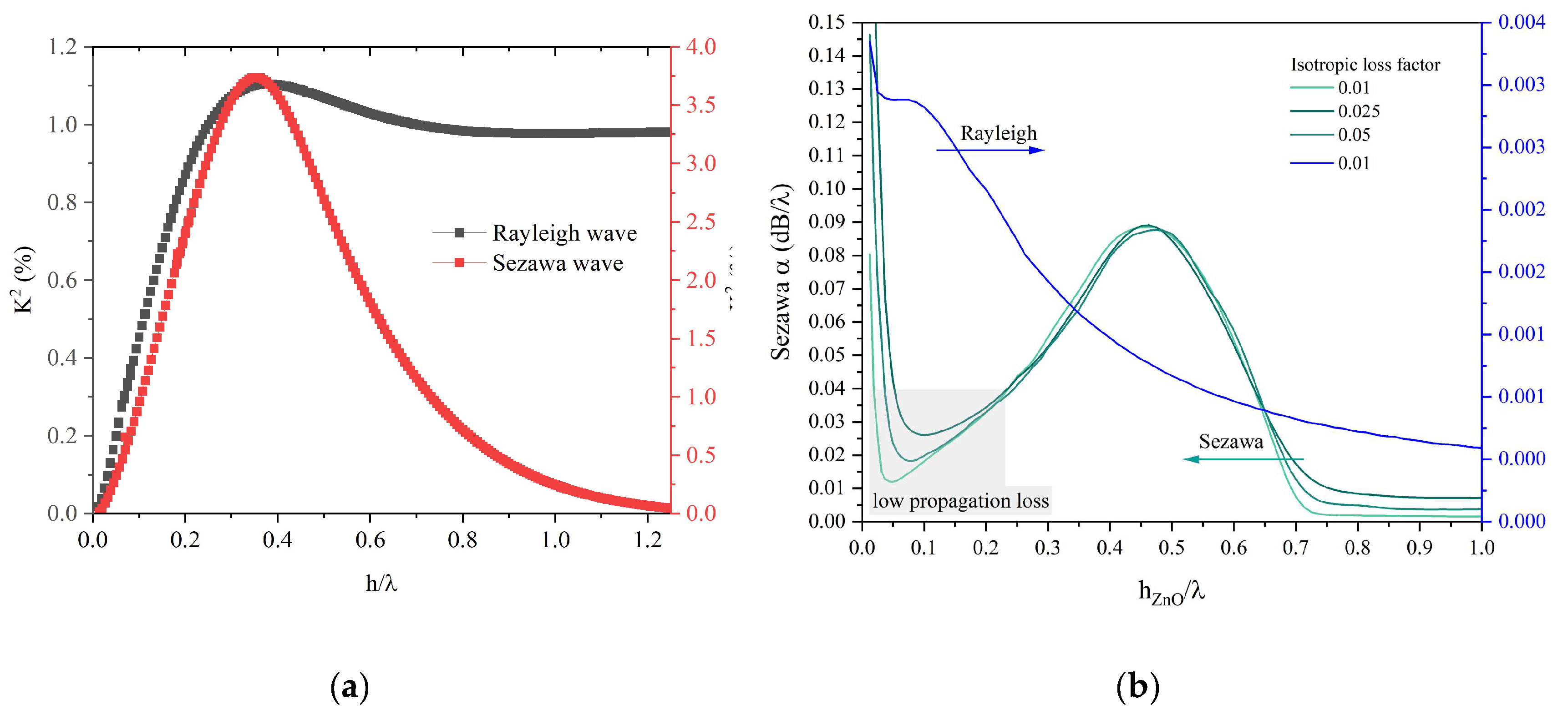
The electromechanical coupling coefficient K2, which is a measure of the electrical-to-acoustic energy conversion efficiency by electrical means, was evaluated from eigenfrequency analysis by calculating the phase velocity of the modes with electrically free (vf) and shorted (vs) boundary condition onto the ZnO free surface ( i n t e r f a c e ) and using the following approximate formula:   K 2 = 2 · v f v s v f . Figure 4a shows the K2 dispersion curves for the Rayleigh and Sezawa waves.
The admittance Y vs frequency curves were calculated by performing the frequency domain study: the waves propagation loss was calculated by applying the formula α = ω 2 Q v g , where ω = 2 π f , v g = v p h + h λ v p h h λ is the group velocity, v p h is the phase velocity, Q = f r f 3 d B [15]; f r and f 3 d B were evaluated from the real part of the Y vs. frequency curve as the abscissa of the peak and as the range of frequencies covered by the half-power bandwidth. Figure 4b shows the propagation loss dispersion curves for the Rayleigh and Sezawa waves for different values of the isotropic loss factor of the SiO2 substrate; the shadowed portion of the α curve highlights a low-loss region for the Sezawa mode.
At very low h/λ ratios, the acoustic penetration depth of the Rayleigh wave extends beyond the interface between the thin film and the substrate, making the substrate crucial for losses. With increasing the layer thickness, the Rayleigh wave experiences a decreasing propagation loss and an increasing K2 which asymptotically reaches that of the ZnO half-space while the propagation loss tends to zero since the wave travels predominantly along the ZnO layer thus it becomes unaffected by the presence of the lossy substrate (the wave suffers only the loss from the layer).
The Sezawa wave is less surfacy than the Rayleigh wave as it travels inside both the substrate and the layer. It has a very low K2 and high propagation loss for very small h/λ since the acoustic penetration depth extends beyond the film/substrate interface. From Figure 4a it can be noticed that, below the cut off h λ c u t   o f f , the K2 of the LS increases and reaches a peak (about 3.7%) at h/λ = 0.375; as h/λ decreases further, the K2 goes to zero because the ZnO layer thins and α increases. For h/λ larger than the cut off, the K2 tends to zero and the loss asymptotically reaches the loss in the substrate since the Sezawa wave is mostly confined in the SiO2 substrate which is non-piezoelectric and lossy.
The α dispersion curves of the Rayleigh and Sezawa waves were calculated for different values of the SiO2 isotropic loss factor ranging from 0.01 up to 0.05. The Rayleigh wave seems to be unaffected by the choice of the substrate loss which is consistent with the surface character of the wave. On the contrary, the Sezawa wave is affected by the SiO2 loss (since the wave mostly travels into the SiO2 substrate) but the shape of the dispersion curve remains unchanged for the different values ​​of the parameter.
From the calculations carried out, it turned out that the Sezawa mode is characterized by a dispersion of leaky waves: the cut-off frequency is not a discrete point in the phase velocity vs. h/λ curves but is a long-period termination of a wave surface that approaches the bulk longitudinal velocity of the substrate with increasing propagation loss except in a small low-loss region whose existence is confirmed by the measured data. Since the low-loss conditions for LS waves propagating in ZnO/SiO2 structure can approach velocity of 5840 m/s (equal to almost double the Rayleigh wave velocity), operation frequencies of several hundreds of MHz are achievable, which are suitable to implement high frequency SAW resonators and sensors.

3. Experimental

3.1. SAW Devices Fabrication

Piezoelectric c-axis oriented zinc oxide (ZnO) thin films, from about 1.8 up to 6.6 µm thick, have been grown by radio frequency (RF) magnetron sputtering (by Ionvac Process s.r.l.) onto fused silica and Si substrates in the same sputtering run. The films were sputtered from a 4″ diameter high-purity (99.999%) zinc target, at 200 °C, in Ar/O2 mixture (ratio 1:4) at pressure 3.7 × 10⁻³ Torr, 200 W rf power.
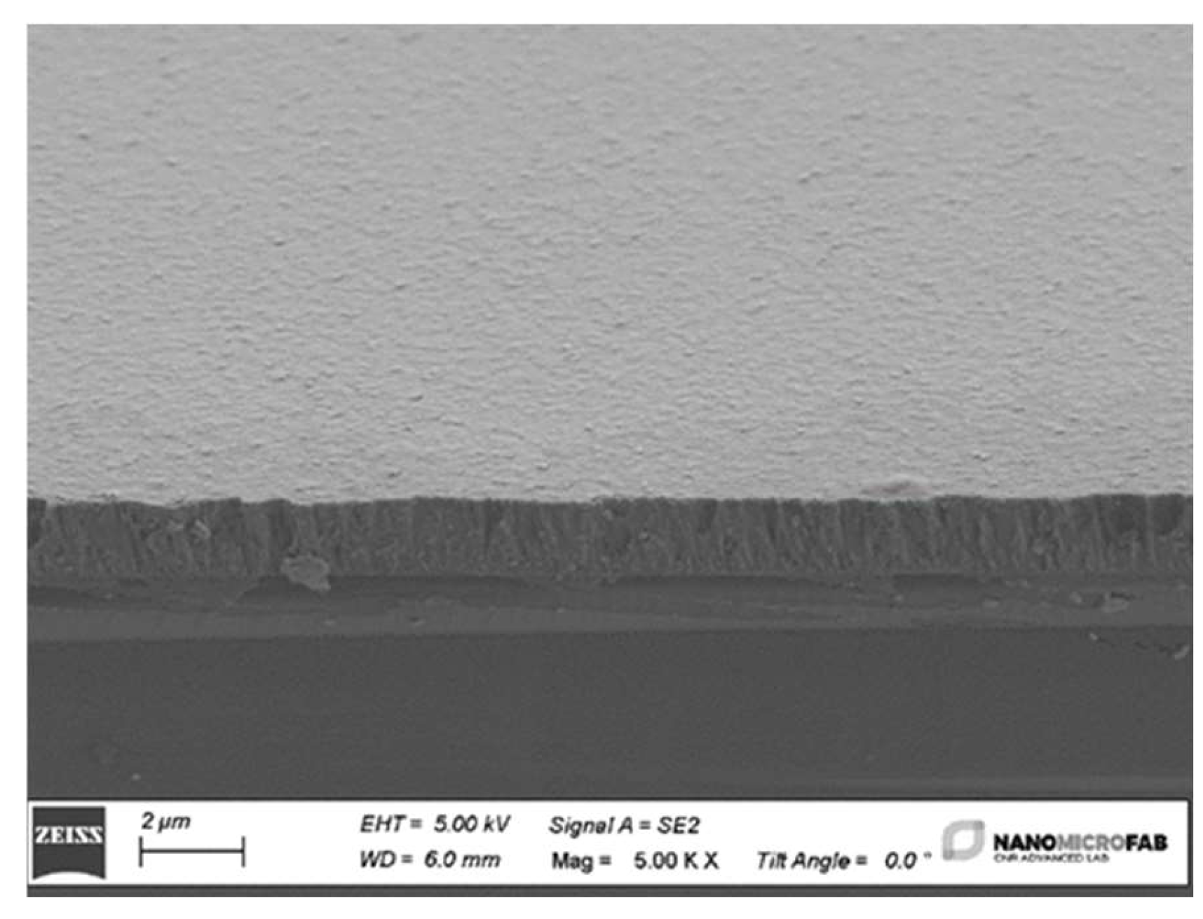
The surface micrographs of the ZnO thin films with various thicknesses were recorded using a scanning electron microscope (SEM) Zeiss Evo MA10 and allowed to estimate the ZnO deposition rate (13.3 nm/min). A representative image of 4 µm thick ZnO thin film, shown in Figure 5, depicts a smooth surface and a columnar structure. The picture highlights both the surface and the cross section of the film and refers to the ZnO film grown onto Si because the latter can be cleaved for cross-sectional imaging more conveniently than fused silica. The ZnO films were c-axis oriented [16], uniform, and highly adhesive to the substrate.
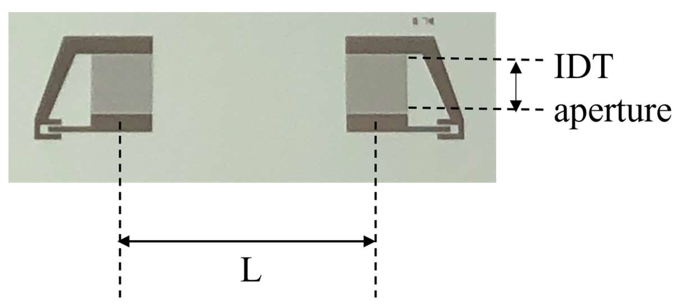
SAW delay lines were photolithographically patterned onto the ZnO free surface by conventional optical lithographic technique and lift-off process. The delay lines consist in a couple of Al IDTs: each IDT consisted of 80 electrodes in split-finger configuration to minimize overall transducer reflection, with an electrode width of 10 μm and a periodicity of λ = 80 μm. The IDT fingers overlapping is 1568 μm and the IDT’s center-to-center distance is L = 6600 μm, as shown in Figure 6. The SAW delay lines were assembled on a printed circuit board (PCB), and the solder pads were electrically bounded to SMA connectors to test their frequency response.

3.2. SAW Devices Test

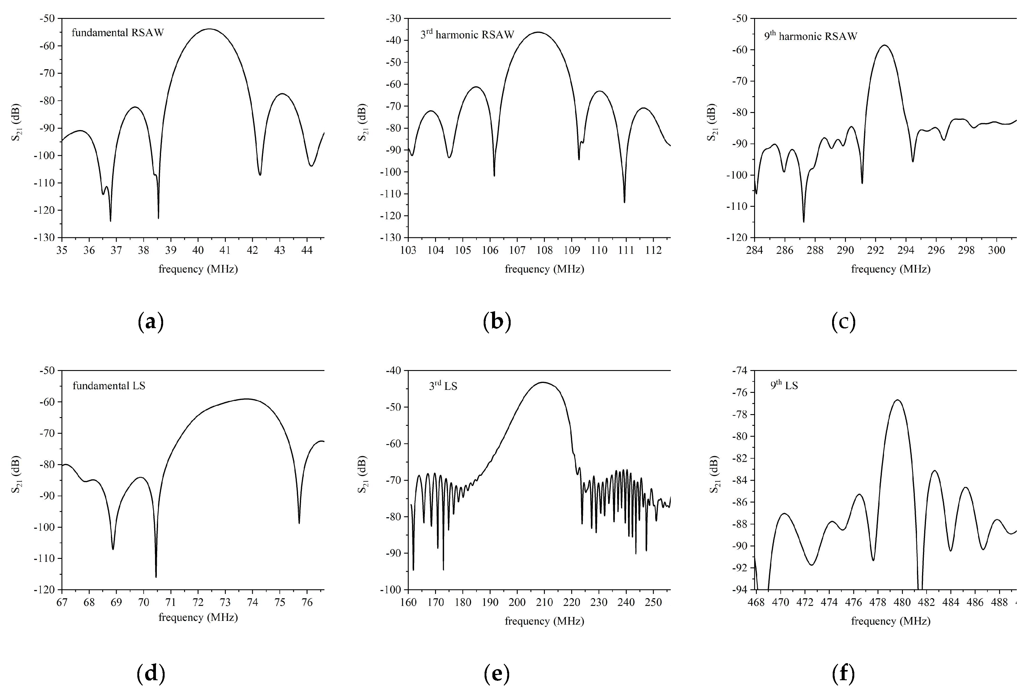
The scattering parameters of the SAW delay lines were tested by means of a vector network analyzer (DG8SAQ VNWA 3 from SDR Kits) in dark, at controlled humidity (40 %) and temperature (24°C). Figure 7 a-f shows, as an example, the S21 vs frequency curves of six modes detected in the bilayer structure, for ZnO film 4 µm thick. The measurements were performed with the VNA calibrated (full two ports calibration) with SOLT kit (SOLT = Short, Open, Load, Through) up to the coaxial cables. The calibration of the VNA excludes the test fixture which consists in two SMA connectors mounted onto the PCB where the ZnO/fused silica substrate is fixed, and the IDTs pads are electrically connected to the SMA connectors by Al wires soldered by ultrasonic bonding. All the curves in Figure 7 a-f were obtained by using the time gating configured to gate out the spurious time signals: the gate center was placed at the peak of the time response and the gate span was adjusted to include all the sidelobes; then, the inverse transform of the gated data was performed to obtain the idealized frequency response.
Several SAW delay lines were tested for different ZnO thicknesses (1.83, 3.1, 4.0, 4.98, 6.6 µm). The frequencies of the fundamental and harmonic modes were measured for both the Rayleigh and LS waves. The experimental modes velocity values, v p h = f · λ , were obtained by multiplying the operating frequency f by the corresponding wavelength; the estimated velocities were plotted inside the graph of Figure 3.

5. Discussions

The propagation of LS waves has been experimentally observed and theoretically predicted in heterostructures comprising a piezoelectric layer and a highly-anisotropic substrate such as SiC, diamond, LiNbO3 and sapphire. Table 1 list some examples of bi-layered structures where the Sezawa waves were observed above the transonic state. The large variety of examples cited in the table, which also includes non-piezoelectric materials, demonstrates that LS waves can be found in both high- and low-symmetry layered structures.
The experimental data listed in Table 1 demonstrate the following key features:
  • Among the listed structures, the ZnO/SiO2 stands out for its technological ease and the low cost of the materials. Indeed, the reactive RF magnetron sputtering technique is a well-established, high-deposition rate, relatively low-temperature (T = 200°C) process which is compatible with standard microelectronic technology. Since the sputtered ZnO films are highly c-axis oriented, uniform and extremely adhesive to the substrate, they can be a valid alternative to thin epitaxial piezoelectric layers deposited using techniques that require expensive and dedicated equipment.
  • Fused silica, unlike expensive and highly anisotropic substrates, is a low cost, optically transparent substrate: its high resistance to chemicals, low coefficient of thermal expansion and excellent optical qualities, make it attractive for applications in optics operating in the deep UV and visible wavelength range [16,25,26].
  • The value of the losses that can be read from the S21 curves of Figure 6 basically comprises 6 dB from IDTs bidirectionality loss (attributed to the SAW propagation toward both sides of each IDT), miscellaneous losses (due to electrical finger resistance and IDTs electrical mismatch with the peripheral circuits), and acoustic propagation loss. The largest contribution to the overall loss, the electrical mismatch of the IDTs with the characteristic impedance of the VNA, comes from using a non-optimized SAW delay line geometry implemented on the tested devices. This geometry is general purpose and not specifically designed for ZnO/SiO2-based devices. By optimizing the IDT parameters (the directivity and the number of finger pairs) on the K2 dispersion curve and possibly adopting a tuning circuit to match the VNA load impedance to the input and output ports, the frequency response of the based devices on LS it can be improved.
According to Figure 6, the IL per wavelength (calculated as IL/Nλ, for Nλ= L/λ) of the Rayleigh and LS waves progresses from - 0.58 to - 0.07 dB/λ, and from - 0.64 to - 0.094 dB/λ with increasing the ZnO h/λ from 0.05 to 0.45 (having subtracted the 6 dB of bidirectionality). These IL values, even including the conversion loss, are just a little higher than those measured in epitaxial ScAlN thin film grown by molecular beam epitaxy on 4H-SiC [15], or in atomically flat AlN grown onto sapphire [27], single-crystal and polycrystalline diamond substrates [28], although an epitaxial piezoelectric film is expected to have lower propagation loss than the sputtered one due to the reduced dislocation density and the smoother surfaces and interfaces. Despite the large IDTs center to center distance (6600 µm), the appearance of the Sezawa wave in all the tested devices indicates high crystal quality and high performance of the SAW devices fabricated. The experimental results clearly show that the Sezawa waves have operating frequency, signal amplitude and electromechanical coupling coefficient higher compared to the Rayleigh mode, which is consistent with our calculations. For these reasons the Sezawa wave is therefore the preferred mode for device applications.

6. Conclusions

This work reports numerical simulations and experimental results on the propagation of Rayleigh and leaky-Sezawa waves in ZnO/fused silica substrates. Highly resistive, c-axis oriented piezoelectric ZnO thin films have been grown by RF reactive magnetron sputtering technique onto fused silica substrates at 200°C. The SAW propagation properties in ZnO/SiO2 have been investigated experimentally for layer thickness ranging from 1.8 up to 6.6 µm. Besides the propagation of the fundamental and harmonic Rayleigh modes, Sezawa modes arise due to the slow sound propagation velocity in ZnO compared with that of the substrate. Despite all the tested devices exhibit layer thickness-to-wavelength ratio values far below the cut-off of the Sezawa mode and despite the very close transverse BAW velocities of the SiO2 and ZnO materials, the propagation of low-attenuated leaky longitudinal waves was clearly observed. The experimental results have been consolidated by comparison with numerical results obtained by a finite element analysis. These simulations allowed us to compare the measured frequencies with the calculated ones and to get deep insight in the nature of the waves. Such high-frequency modes, identified as leaky-Sezawa (LS) waves under cut-off, are supposed to be excited by the fundamental and harmonic wavelengths of the IDTs: due to their h/λ values smaller than the h λ c u t   o f f , these waves leak energy into the bulk and show predominant longitudinal character when approaching the velocity of the longitudinal BAW in the substrate. The waves propagation in ZnO/fused silica was simulated by using 2D FEM technique to differentiate the type of the guided surface modes in terms of Rayleigh and LS modes. The LS modes velocity is almost double that of the Rayleigh velocity in the substrate which leads to enhanced operation frequency of the SAW devices without requiring expensive nanofabrication techniques necessary to reduce the dimensions of the metal electrodes. Although these fast leaky modes have appreciable penetration into the substrate, their transmission amplitudes are high enough for them to be detected by the receiving IDT and have a quite large electromechanical coupling coefficient. A good agreement between the calculated and measured LS wave velocities has been observed which allowed us to assess the existence of a low-loss region below the cut off.
The LS waves can be of practical utility if exploited in SAW signal processing devices that operate at elevated frequencies; indeed, these waves appearing in “slow on fast” structures can be an alternative path to further increase the operating frequency of SAW devices. Moreover, the combination of split IDTs with a slow-on-fast substrate allows the fabrication of multi-frequency ZnO/SiO2 single device structures which can represent a promising solution for the development of a multi-parameters sensing platform [2,29]; multiple excitation frequencies with different sensing properties can allow the parallel analysis of the same measurand with improved accuracy.

Author Contributions

C.C. conceived the research, wrote the paper; C.C. and D.C. sputtered the ZnO films; D.C. fabricated the devices and did the SEM photos; C.C., M.B. and F.L. performed the theoretical calculations; M.B. designed the SAW device; all the authors performed the SAW sensors’ measurements and elaborated the data. All authors have read and agreed to the published version of the manuscript.

Funding

This research was funded by Ecosystem Rome Technopole project EC00000024, Spoke 6, funded by the European Union – Next Generation EU, PNRR Mission 4 Component 2 Investment 1.5.

Data Availability Statement

Data Availability Statements are available in section “MDPI Research Data Policies” at https://www.mdpi.com/ethics.

Conflicts of Interest

The authors declare no conflicts of interest. .

References

  1. Adler, E.L.; Farnell, G.W.; Galligan, J.M.; Joyce, G.C.; N-Nagy, F.L.; Sittig, E.K.; Spencer, W.J.; Suenaga, M. In Physical Acoustics: Principles and Methods, Mason, W.P., Thurston, R.N., Eds.; Academic Press: London, UK, 1972; Volume IX.
  2. Caliendo, C.; Laidoudi, F. Experimental and Theoretical Study of Multifrequency Surface Acoustic Wave Devices in a Single Si/SiO2/ZnO Piezoelectric Structure. 2020, 20, 1380. [CrossRef]
  3. Pedrós, J.; Calle, F.; Grajal, J.; Jiménez Riobóo, R.J.; Takagaki, Y.; Ploog, K.H.; Bougrioua, Z. Anisotropy-induced polarization mixture of surface acoustic waves in $\mathrm{Ga}\mathrm{N}∕c$-sapphire heterostructures. Physical Review B 2005, 72, 075306. [CrossRef]
  4. Rodriguez-Madrid, J.G.; Iriarte, G.F.; Pedros, J.; Williams, O.A.; Brink, D.; Calle, F. Super-High-Frequency SAW Resonators on AlN/Diamond. Ieee Electron Device Letters 2012, 33, 495–497. [Google Scholar] [CrossRef]
  5. Glushkov, E.; Glushkova, N.; Zhang, C. Surface and pseudo-surface acoustic waves piezoelectrically excited in diamond-based structures. Journal of Applied Physics 2012, 112. [Google Scholar] [CrossRef]
  6. Takagaki, Y.; Santos, P.V.; Wiebicke, E.; Brandt, O.; Schönherr, H.P.; Ploog, K.H. Guided propagation of surface acoustic waves in AlN and GaN films grown on $4H--\mathrm{SiC}(0001)$ substrates. Physical Review B 2002, 66, 155439. [Google Scholar] [CrossRef]
  7. Pedrós, J.; Calle, F.; Grajal, J.; Jiménez Riobóo, R.J.; Prieto, C.; Pau, J.L.; Pereiro, J.; Hermann, M.; Eickhoff, M.; Bougrioua, Z. Anisotropic propagation of surface acoustic waves on nitride layers. Superlattices and Microstructures 2004, 36, 815–823. [Google Scholar] [CrossRef]
  8. Ralib, A.A.M.; Nordin, A.N.; Alam, A.H.M.Z.; Hashim, U.; Othman, R. Piezoelectric thin films for double electrode CMOS MEMS surface acoustic wave (SAW) resonator. Microsystem Technologies 2015, 21, 1931–1940. [Google Scholar] [CrossRef]
  9. Morgan, D. Surface Acoustic Wave Filters, 2nd Edition ed.; Academic Press: Amsterdam (NL), 2007.
  10. Datta, S. Surface Acoustic Wave Devices; Prentice-Hall: 1986.
  11. Morgan, D.P. Quasi-static analysis of floating-electrode unidirectional SAW transducers (FEUDT's). In Proceedings of the 1999 IEEE Ultrasonics Symposium. Proceedings. International Symposium (Cat. No.99CH37027), 17-20 Oct. 1999, 1999; pp. 107-111 vol.101.
  12. Morgan, D.P. Quasi-static analysis of floating electrode unidirectional SAW transducers. IEEE Transactions on Ultrasonics, Ferroelectrics, and Frequency Control 2001, 48, 1289–1297. [Google Scholar] [CrossRef] [PubMed]
  13. Royer, D.; Dieulesaint, E. Free and Guided Propagation. In Elastic Waves in Solids; Springer-Verlag Berlin Heidelberg New York, 2000; Volume I.
  14. Engan, H. Excitation of elastic surface waves by spatial harmonics of interdigital transducers. IEEE Transactions on Electron Devices 1969, 16, 1014–1017. [Google Scholar] [CrossRef]
  15. Gokhale, V.J.; Downey, B.P.; Hardy, M.T.; Jin, E.N.; Roussos, J.A.; Meyer, D.J. Epitaxial Single-Crystal ScAlN on 4H-SiC for High-Velocity, Low-Loss SAW Devices. In Proceedings of the 2020 IEEE 33rd International Conference on Micro Electro Mechanical Systems (MEMS), 18-22 Jan. 2020, 2020; pp. 1262-1265.
  16. Caliendo, C.; Benetti, M.; Cannatà, D.; Buzzin, A.; Grossi, F.; Verona, E.; de Cesare, G. UV Sensor Based on Surface Acoustic Waves in ZnO/Fused Silica. Sensors 2023, 23. [Google Scholar] [CrossRef] [PubMed]
  17. Benetti, M.; Cannata, D.; Di Pietrantonio, F.; Fedosov, V.I.; Verona, E.; Ieee. Theoretical and experimental investigation of PSAW and SAW properties of AlN films on isotropic diamond substrates. In 2005 Ieee Ultrasonics Symposium, Vols 1-4; Ultrasonics Symposium; 2005; pp. 1868-1871.
  18. Aubert, T.; Naumenko, N.; Bartoli, F.; Pigeat, P.; Streque, J.; Ghanbaja, J.; Elmazria, O. Non-leaky longitudinal acoustic modes in ScxAl1-xN/sapphire structure for high-temperature sensor applications. Applied Physics Letters 2019, 115. [Google Scholar] [CrossRef]
  19. Naumenko, N.F.; Didenko, I.S. High-velocity surface acoustic waves in diamond and sapphire with zinc oxide film. Applied Physics Letters 1999, 75, 3029–3031. [Google Scholar] [CrossRef]
  20. Every, A.G.; Maznev, A.A. Fano line shapes of leaky surface acoustic waves extending from supersonic surface wave points. Wave Motion 2018, 79, 1–9. [Google Scholar] [CrossRef]
  21. Kushibiki, J.; Ishikawa, T.; Chubachi, N. Cut-off characteristics of leaky Sezawa and pseudo-Sezawa wave modes for thin-film characterization. Applied Physics Letters 1990, 57, 1967–1969. [Google Scholar] [CrossRef]
  22. Suenaga, R.; Suzuki, M.; Kakio, S.; Ohashi, Y.; Arakawa, M.; Kushibiki, J.-i. Propagation properties of leaky surface acoustic wave on water-loaded piezoelectric substrate. Japanese Journal of Applied Physics 2018, 57, 07LC10. [Google Scholar] [CrossRef]
  23. Valle, S.; Singh, M.; Cryan, M.J.; Kuball, M.; Balram, K.C. High frequency guided mode resonances in mass-loaded, thin film gallium nitride surface acoustic wave devices. Applied Physics Letters 2019, 115, 212104. [Google Scholar] [CrossRef]
  24. Fu, S.; Wang, W.; Qian, L.; Li, Q.; Lu, Z.; Shen, J.; Song, C.; Zeng, F.; Pan, F. High-Frequency Surface Acoustic Wave Devices Based on ZnO/SiC Layered Structure. IEEE Electron Device Letters 2019, 40, 103–106. [Google Scholar] [CrossRef]
  25. Buzzin, A.; Grossi, F.; Cannatà, D.; Benetti, M.; Cesare, G.d.; Caliendo, C. ZnO based Back- and Front-Illuminated Photoresistor for UV Sensing Applications. In Proceedings of the 2023 9th International Workshop on Advances in Sensors and Interfaces (IWASI), 8-9 June 2023, 2023; pp. 273-276.
  26. Caliendo, C.; Cannatà, D.; Benetti, M.; Buzzin, A. UV sensors based on the propagation of the fundamental and third harmonic Rayleigh waves in ZnO/fused silica. In Proceedings of the 2023 9th International Workshop on Advances in Sensors and Interfaces (IWASI), 8-9 June 2023, 2023; pp. 261-266.
  27. Uehara, K.; Aota, Y.; Shibata, T.; Kameda, S.; Nakase, H.; Isota, Y.; Tsubouchi, K. Surface Acoustic Wave Properties of Atomically Flat-Surface Aluminum Nitride Epitaxial Film on Sapphire. Japanese Journal of Applied Physics 2005, 44, 4512. [Google Scholar] [CrossRef]
  28. Fujii, S.; Yamada, H.; Omori, T.; Hashimoto, K.y.; Torii, H.; Umezawa, H.; Shikata, S.i. One-port SAW resonators fabricated on single-crystal diamond. In Proceedings of the 2013 IEEE MTT-S International Microwave Symposium Digest (MTT), 2-7 June 2013, 2013; pp. 1-3.
  29. Caliendo, C.; Hamidullah, M. A Theoretical Study of Love Wave Sensors Based on ZnO–Glass Layered Structures for Application to Liquid Environments. 2016, 6, 59.
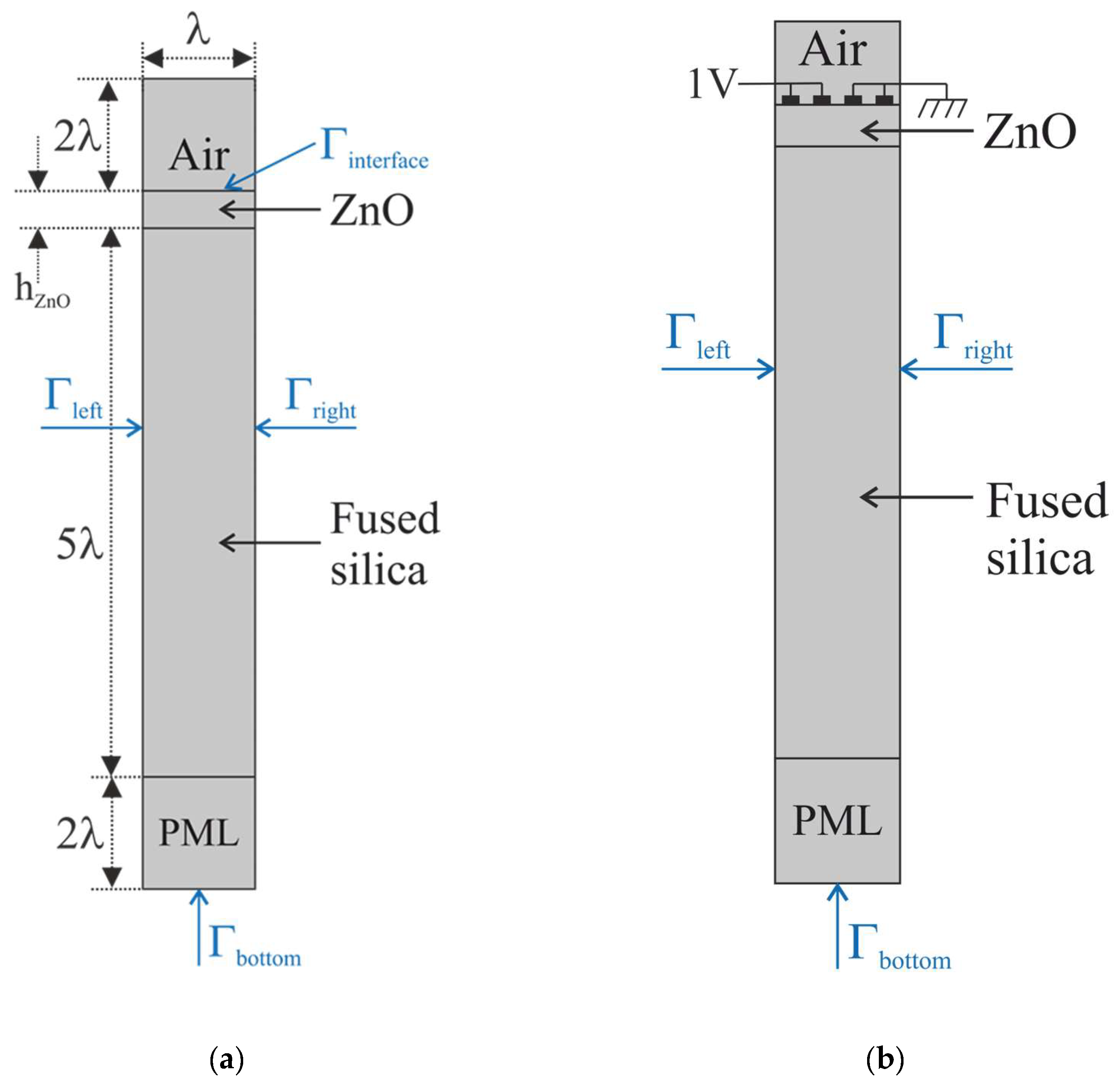
Figure 1. (a) The unit cell (not in scale) consisting in four domains: Air (2·λ thick), ZnO (from 1 to 80 µm thick), SiO2 (5·λ thick) and PML (2·λ thick); (b) the unit cell including the Al electrodes.
Preprints 110312 g001
Figure 2. a) The solid displacement, b) the longitudinal and c) shear displacement component of the leaky Sezawa wave.
Preprints 110312 g002
Figure 3. The theoretical phase velocity dispersion curves of the Rayleigh and Sezawa modes travelling in the ZnO/SiO2 structure; the black points are referred to the experimental measures.
Preprints 110312 g003
Figure 4. (a) The theoretical K2 vs the ZnO h/λ curves of the Rayleigh and Sezawa modes travelling in the ZnO/SiO2 structure. (b) The propagation loss dispersion curves for the Rayleigh and Sezawa waves; the isotropic loss factor of the SiO2 substrate is the running parameter.
Preprints 110312 g004
Figure 5. The SEM photo of the surface and cross section of the ZnO/SiO2 structure.
Preprints 110312 g005
Figure 6. The picture of the SAW delay line implemented onto ZnO/fused silica substrate.
Preprints 110312 g006
Figure 7. The frequencies corresponding to the surface modes experimentally detected in ZnO(4µm)/SiO2 are the following: a) 40.41, b) 73.5, c) 107.75, d) 292.6, e) 209.70, and f) 479.64 MHz.
Preprints 110312 g007
Table 1. The medium where the LS propagates, the film normalized thickness and the reference.
Propagating medium h/λ Reference
GaN/sapphire(11-20) 0.2125 [7]
GaN/sapphire 0.125 – 0.875 [7]
AlN(0001)/diamond(111) 0.1875 – 0.75 [4]
AlN/Diamond 0.15 [5]
AlN/iso-Diamond * [5]
AlN/iso-Diamond/c-TiAl * [5]
AlN/diamond 0.09 [17]
AlN/4H–SiC(0001)[1-100] 0.3-0.5 [6]
GaN/4H–SiC(0001)[11-20] ~0.7 [6]
Sc0.09Al0.91N/c-sapphire 0.425 [18]
ZnO/(001)<110>diamond * [19]
Iso-Cd/iso-Cr Appr. 0.08 [20]
Au/fused quartz 0.0328 [21]
a-SiO2/128°YX-LiNbO3 0.41 and 0.62 [22]
ScAlN/4H-SiC 0.1, 0.12 and 0.17 [15]
GaN/SiC from 0.2 to 0.48 [23]
ZnO/SiC ~0.1 [24]
ZnO/fused silica 0.05 to x Present paper
* Theoretical paper.
Disclaimer/Publisher’s Note: The statements, opinions and data contained in all publications are solely those of the individual author(s) and contributor(s) and not of MDPI and/or the editor(s). MDPI and/or the editor(s) disclaim responsibility for any injury to people or property resulting from any ideas, methods, instructions or products referred to in the content.
Copyright: This open access article is published under a Creative Commons CC BY 4.0 license, which permit the free download, distribution, and reuse, provided that the author and preprint are cited in any reuse.
Prerpints.org logo

Preprints.org is a free preprint server supported by MDPI in Basel, Switzerland.

Subscribe

© 2024 MDPI (Basel, Switzerland) unless otherwise stated