Preprint
Review

A Survey on Neuromorphic Architectures for Running Artificial Intelligence Algorithms

Altmetrics

Downloads

318

Views

160

Comments

0

A peer-reviewed article of this preprint also exists.

Submitted:

30 June 2024

Posted:

01 July 2024

You are already at the latest version

Alerts
Abstract
Neuromorphic computing, a brain inspired non-Von Neumann computing system, addresses the challenges posed by the Moore’s law memory wall phenomenon. It has the capability to increasingly enhance performance while maintaining power efficiency. Neuromorphic chip architecture requirements vary depending on the application and optimizing it for large-scale applications remains to be a challenge. Neuromorphic chips are programmed using spiking neural networks which provide them with important properties such as parallelism, asynchronism, and on-device learning. Widely used spiking neuron models include the Hodgkin-Huxley Model, Izhikevich model, integrate-and-fire model and spike response model. Hardware implementation platforms of the chip follow three approaches: analog, digital, or a combination of both. Each platform can be implemented using various memory topologies which interconnects with the learning mechanism. Current neuromorphic computing systems typically use the unsupervised learning spike timing-dependent plasticity algorithms. However, algorithms such as voltage-dependent synaptic plasticity have the potential to enhance performance. This review summarizes the potential neuromorphic chip architecture specifications and highlights which applications they are suitable for.
Keywords: 
Subject: Engineering  -   Electrical and Electronic Engineering

1. Introduction

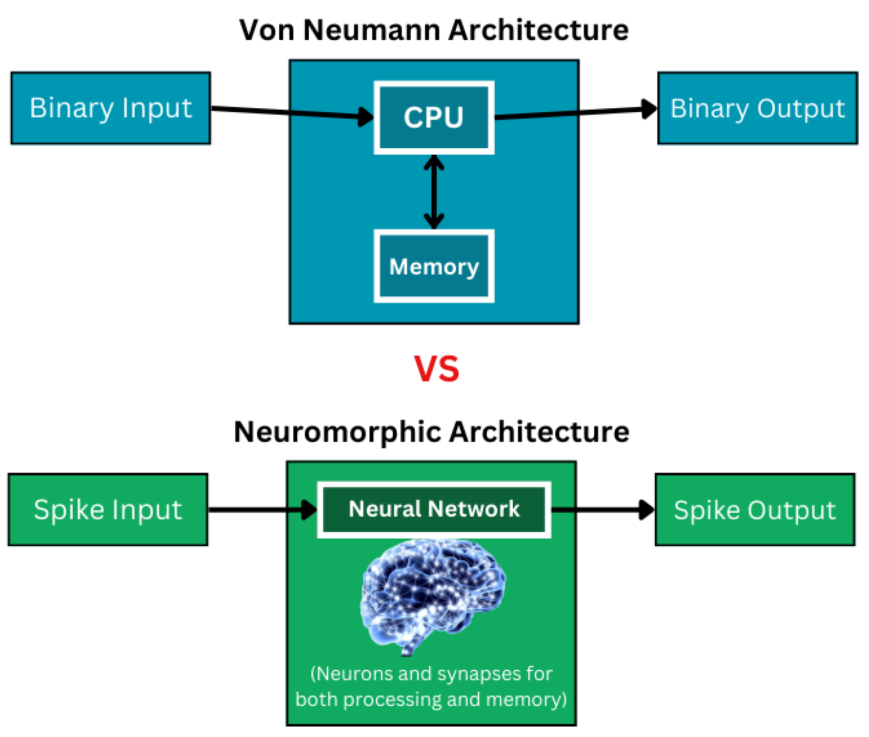
Artificial intelligence (AI) is a continuously emerging field that is commonly used for various applications and purposes. Conventional technologies used for running complex AI algorithms utilize Von Neumann computers which have a high rate of power consumption and cause a carbon emission problem. As stated in article [1], training a single deep learning (DL) model can equate to the same amount of total lifetime carbon footprint of five cars and has approximately 656,347 kilowatt-hours of energy consumption [1]. In addition, recent advancements in computing speed and capacity have reached a saturation level in performance due to the continuous application of Moore’s law which resulted in the memory wall phenomenon. Moore’s law refers to the decrease in size of transistors on digital integrated chips to achieve a faster performance. This also resulted in an increase of data movement and as computational speed continuously increased, memory performance overall remained the same leading to the memory wall phenomenon and saturations of the system’s performance [2]. As AI algorithms continue to evolve a new technology that meets the high performance, energy efficiency and large bandwidth requirements is needed [3]. Neuromorphic computing, which is a brain-inspired computing system has the capability to increasingly enhance performance at a decreasing level of power consumption. Neuromorphic computers are non-Von Neumann computers which are composed of neurons and synapses as opposed to separate CPUs and memory units [4].
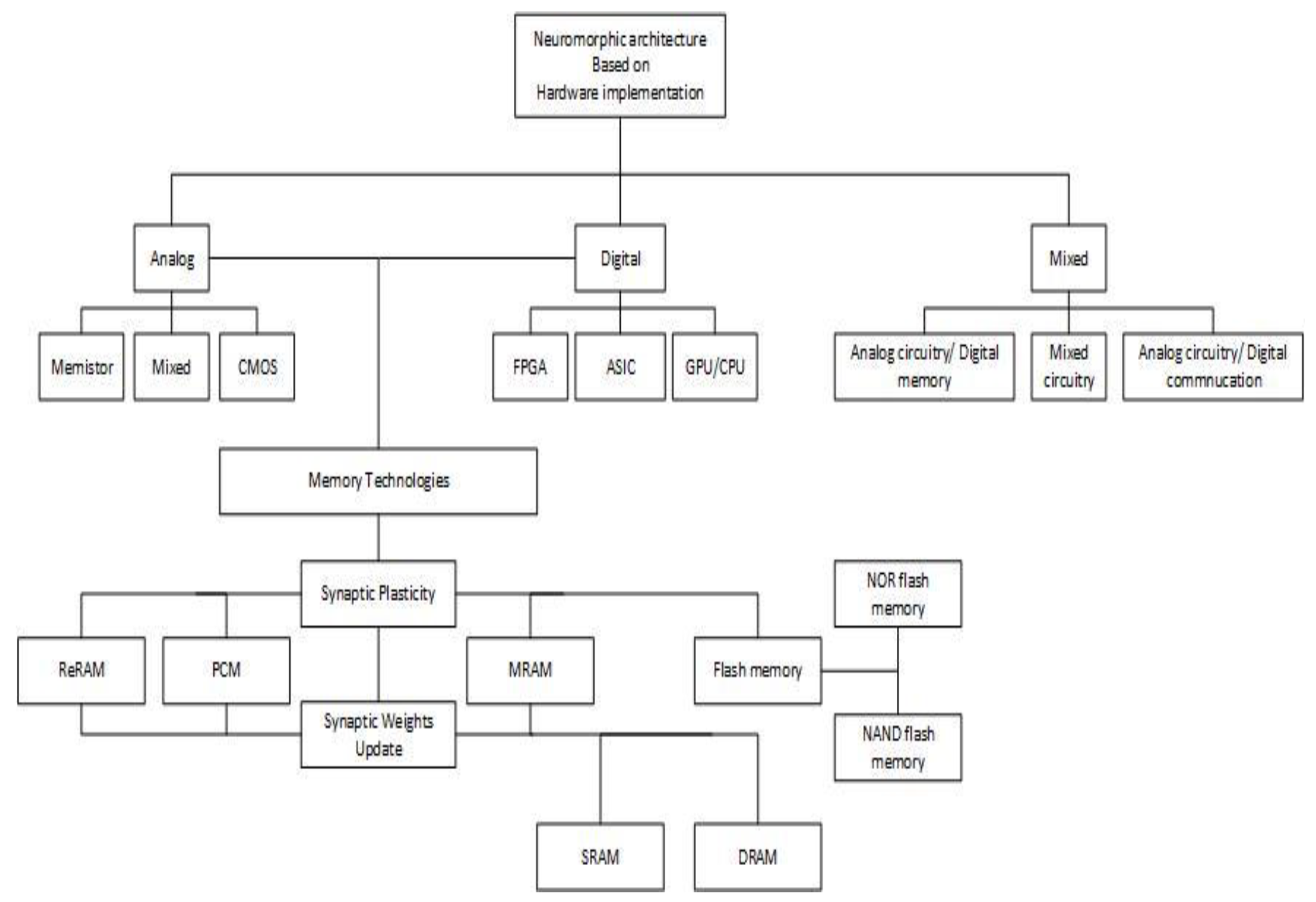
Neuromorphic chips are programed using spiking neural networks (SNNs) which provide a more energy efficient, computationally powerful network and fast and massively parallel data processing compared to artificial neural networks (ANNs). They are implemented using one of the four main spiking neuron models (shown in Figure 1) which include the Hodgkin-Huxley (HH) model, Izhikevich model, integrate-and-fire (IF) model and spike response model (SRM). These models closely exhibit biological neurons characteristics and behaviours [5,6]. In neuromorphic computing, various architectures can be developed based on the hardware implementation platform, network topologies, and neural models. Hardware implementation platforms follow three approaches: analog, digital, and a combination of both, as depicted in Figure 2. The subsections of a neuromorphic unit include the computational unit (neural model), the information storage unit (synaptic model), the communication unit (dendrites and axons), and the learning mechanism (weights update). Considering the advantages of both digital and analog implementation methods, they can be combined or used separately to implement the subsections of neuromorphic computing hardware. Additionally, various memory technologies can be employed in both analog and digital systems for two important reasons: synaptic plasticity (non-volatile information storage) and weight updates (fast read and write capabilities), as presented in Figure 2.
An analog device for neuromorphic computing is a more cost-effective approach compared to digital design and can provide in memory computing but lacks flexibility. In a digital implementation, data exchange is required between the Arithmetic Logic Unit (ALU) and memory cells making its implementation at a large-scale challenging. However, a digital implementation has the ability to implement almost any learning algorithm and allows for more customization and flexibility [7]. A mixed design approach which includes the advantages of both analog and digital implementation can overcome several limitations. Digital communication stored in the form of digital spikes can be utilized for analog neuromorphic systems, increasing the duration of storage of the synaptic weights and the reliability of the system [8].
Analog circuits for neuromorphic computing can be implemented using Memristors, CMOS or Resistive RAM. Memristors are an emerging memory device with a memristive memory and have a fast operation speed, low energy consumption and small feature size. They have a switching mechanism between states through programming pulses. They can be classified into nonvolatile and volatile types, where the nonvolatile is capable in developing in-memory computing and the volatile is typically utilized for synapse emulators, selectors, hardware security and artificial neurons [9,10]. Complementary metal oxide semiconductor (CMOS) transistors have been successfully used to implement neurons and synapses for neuromorphic architecture. In addition, they are widely used for large-scale spiking neural networks (SNNs) [11]. Lastly, resistive access memory (ReRAM) is a two-terminal nanodevice that is promising for neuromorphic computing as it can enable highly parallel, ultra-low-power computing in memory for AI algorithms. It is structurally simple and thus can be easily integrated into the system at a low power consumption [12].
A digital implementation of neuromorphic architecture can be completed through the use of FPGAs, ASIC or a heterogenous system composed of CPUs and GPUs. Field-programmable gate arrays (FPGAs) provide several advantages for neuromorphic computing which include flexibility, high performance and reconfiguration capability and excellent stability. In addition, they can implement SNNs due to their parallel processing ability and sufficient size of local memory to restore weights. Recent implementations of FPGA-based neuromorphic systems utilize random access memory (RAM) to optimize the latency of memory access [6]. Application Specific Integrated Circuit (ASIC) implementations of neuromorphic systems are less flexible, have a higher production cost compared to FPGA and are limited to specific neuron models and algorithms [6,8]. However, ASIC provides low power consumption and a high-density local memory which are attractive features for neuromorphic systems development [13]. Modern ASICs include flash memory as they have a long retention time (>10 years). Flash memory has a three-terminal structure, is charge-based and a nonvolatile memory [5]. A heterogenous system architecture composed of both Central Processing Units (CPUs) and Graphics Processing Units (GPUs) for neuromorphic computing can provide flexibility in the programming due to the CPUs as well as parallel processing and accelerated computing due to the GPUs [14]. However, they cannot be easily scaled due to their high energy demands [13]. RAM or ReRAM can be utilized for the heterogenous system to store the weights [15].
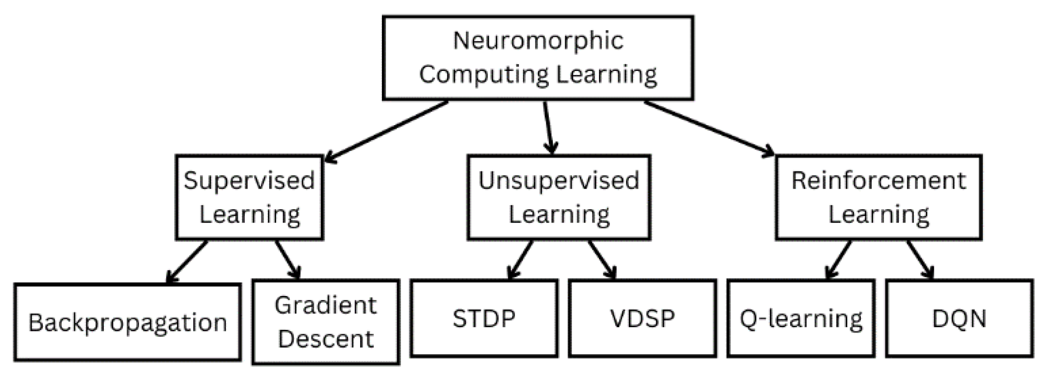
As illustrated in Figure 3, there are three main different machine learning methods that are commonly used: supervised learning, unsupervised learning, and reinforcement learning [6]. Non-machine learning methods are less common but can also be used for neuromorphic computing for applications that solve a particular task [4]. Learning mechanisms are an essential step for developing neuromorphic systems as they are used to adapt to the specified application. On-chip training is extremely desired for many applications and refers to learning in a neuromorphic chip. Off-chip training is when learning is implemented externally through software for example and the weights are then postprocessed and used to fabricate the neuromorphic system [6].
Supervised learning is the training of data using labelled datasets and can be divided into backpropagation and gradient descent algorithms. Unsupervised learning is the training of data with an unlabeled dataset and can be divided into STDP and VDSP algorithms. Lastly, Reinforcement learning is when the machine learning algorithm learns from experiences and feedback without any labelled data. It is an iterative long-term process and can be divided into Q-learning and DQN algorithms [16].
Neuromorphic computing can be used for various applications and industries which include medical, large-scale operations and product customization, artificial intelligence, and imaging. Its design parameters ultimately depend on the desired application and several companies have implemented a neuromorphic chip each with different architectures to solve different tasks [16] This review focuses on the various possible neuromorphic chip architectures and their capabilities.

2. Background

Neuromorphic chips consist of artificial neurons and synapses to achieve similar functions to the human brain. There are 1010 – 1012 neurons in the human brain that each have 104 synaptic connections operating simultaneously and communicating with each other through spike signals. The human brain inspired the development of this chip due to its ability to perform high-order intelligence tasks at a low energy consumption rate [5]. Neuromorphic chips are defined as non-von Neumann due to the governing of both processor and memory by neurons and synapses and reception of inputs as spikes. They have a parallel operation and are asynchronous (event-driven). Controversy, Von Neumann computers are composed of separate CPUs and memory units, and information is encoded as numerical values. They perform sequential processing and are synchronous (clock-driven) [4]. The main differences between Von Neumann architecture and Neuromorphic architecture are illustrated in Figure 4.
Neuromorphic chips provide various advantages over current Von Neumann computers due to their operations properties which include:
  • Connectionism: is described using neural networks (NN) which consist of many simple units (neurons) interconnected together with weights. Determining the appropriate weights results in the NNs ability to learn and solve a given problem [7].
  • Parallelism: all neurons work in parallel to each other to simultaneously perform various functions and ensure efficient and successful operation of neural networks [7].
  • Asynchrony: to achieve parallelism, synchronization of all neurons is not required as each neuron performs a specified task. Asynchrony reduces the power consumption that would otherwise be required to achieve synchronization [7].
  • Impulse nature of information transmission: the information encoded as spikes differs between different pairs of neurons and does not occur instantly. A synapse is therefore characterized by the weight and time delay and provides advantages over traditional neural networks. It is asynchronous, allows the use of dynamic data due to its inclusion of the time component, it is a complex non-linear dynamic system, and the neuron is only activated upon the receival of a spike, reducing the power consumption as its inactive state does not consume a large amount of energy [7].
  • On-device learning: it has the ability to learn in a continuous and incremental manner which in turn allows the customization and personalization of smart devices based on the user needs while maintaining privacy through the avoidance of user data transmission to the cloud [7].
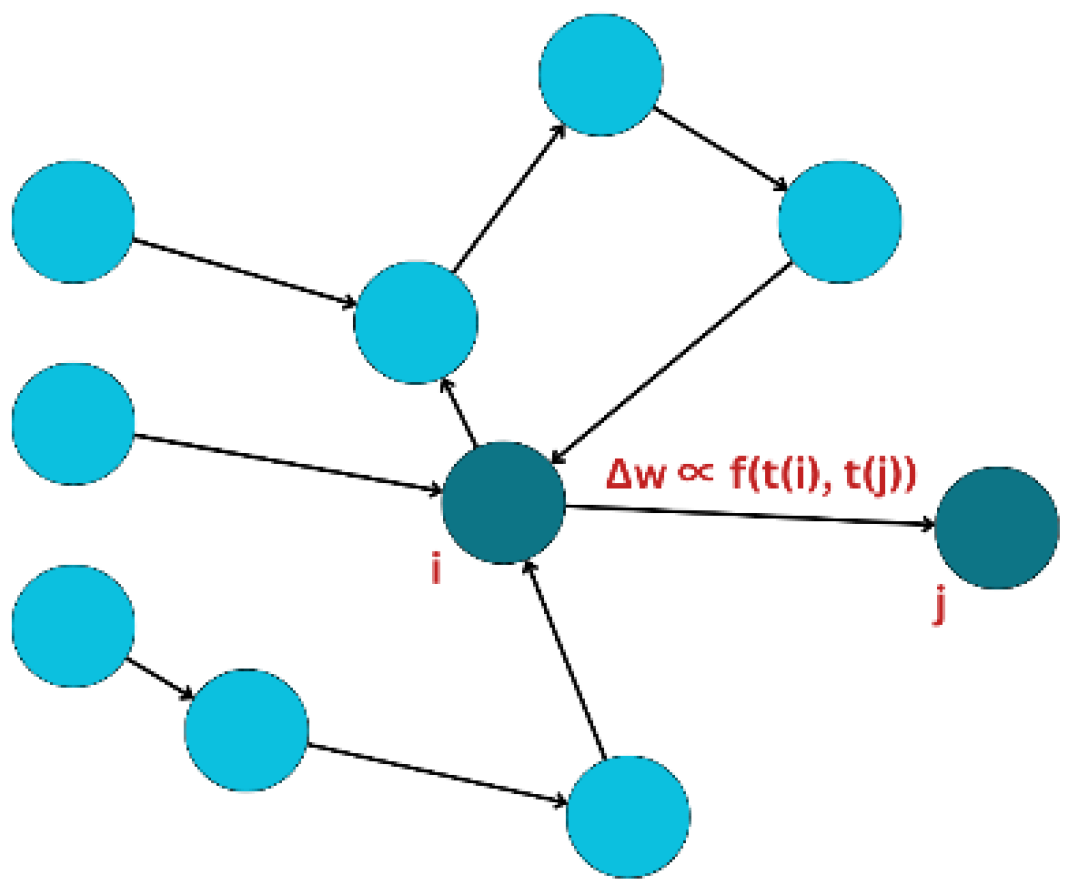
  • Local learning: conventional neural networks use backpropagation algorithms which introduce two problems: the weight transport problem and the update locking problem. The weight transport problem is the system’s inability to exchange information about the weight value and the update locking problem is the requirement of forward pass activation values to be stored for backward pass. Local learning is an alternative to backpropagation and uses a Spike timing Dependent Plasticity (STDP) model where the synapses are strengthened upon receival of a spike before the neuron generated the spike or weekend if the spike was received after the neuron generated the spike. As a result, local learning can train any size of network as it does not require large amounts of global data transfer operations [7].
  • Sparsity: not all neurons are activated to perform a task. Neuromorphic chips have temporal, spatial and structural sparsity. Temporal sparsity is the data sparse in time which is determined by the transmission of only the changed part of a signal. Spatial sparsity is sparsity in data streams resulted by neurons activated only upon reaching a certain threshold value. Structural sparsity refers to the data flow with respect to the network topology, as each neuron has a limited number of connections, and they are not all fully interconnected together [7].
  • Analog computing: digital computing is limited due to its high costs. Analog circuits can be used to model the dynamics of the membrane potential and to model synaptic operations. Analog circuits provide a more time and energy efficient alternative.
  • In-memory computing: each individual neuron has its own memory or stored state which eliminates the need for transferring intermediate data or the competitive memory access [7].

2.1. Spiking Neural Networks (SNN)

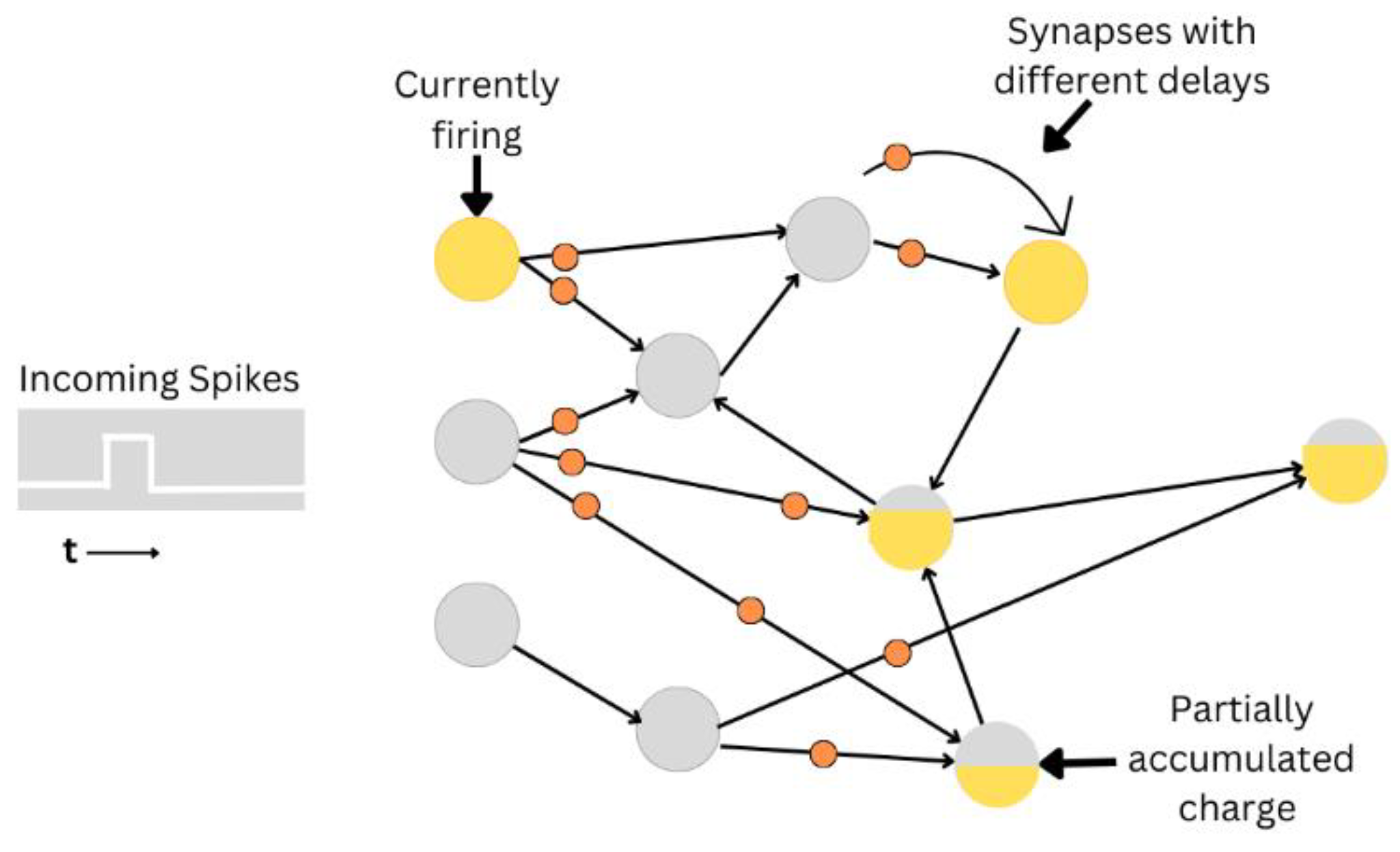
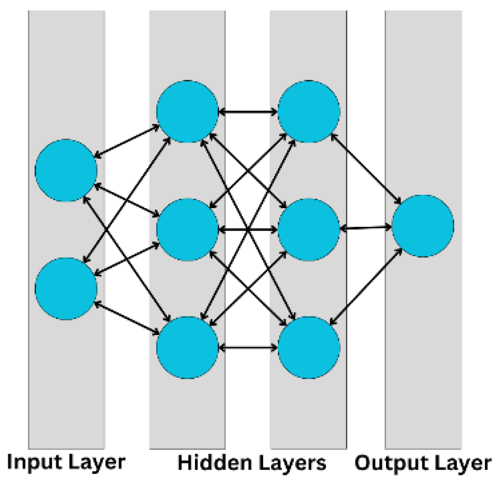
Neuromorphic chips are programed using spiking neural networks (SNNs) rather than artificial neural networks (ANNs) due to their biological functionalities and employment of biological neuron models such as the integrate-and-fire model, leaky integrate-and-fire (LIF) model, and Izhikevich model which all allow the communication between neurons through the generation of spike signals [5]. SNNs provide a more energy efficient, computationally powerful network and fast and massively parallel data processing for neuromorphic chips compared to ANNs. They are implemented using differential equations and have memory while ANNs are implemented using activations functions and have no memory [6]. The spike signals sent to a neuron accumulate in the neuron membrane potential and the signal is passed to other connected neurons only when the membrane potential reaches a certain threshold [5]. A charge leakage that dissipated overtime can occur if the threshold is not reached. In addition, outgoing synapses can be affected due to axonal delays which in turn results in information delay. Figure 5 illustrates the pre-synaptic and post-synaptic neurons connected by the synapses which carry the associated weight value. The weight value is excitatory if positive or inhibitory if negative. The synapses are trained using the selected learning mechanisms to alter the weights and activate the synapse only when needed. SNNs are organized into layers and their capability to transmit information at different times is known as the asynchronous function of neuromorphic chips which aids in reducing power consumption [4].
challenging to implement on classical von Neumann architecture (CPUs/GPUs) due to the large demands of power and time. Hence, FPGA or ASICs which can offer a high-speed and low-power hardware implementations of SNNs are a good alternative for large-scale implementations [6]. Other implementations are completed using memristors combined with STDP [7].

2.2. Spiking Neuron Models

Four popular and widely used spiking neuron models include the Hodgkin-Huxley (HH) model, Izhikevich model, integrate-and-fire (IF) model and spike response model (SRM). These models closely exhibit biological neurons characteristics and behaviours. While ANN models include sigmoid, rectified linear unit (ReLU) or tanh, which are computation units [6].
The first developed model of a spiking neuron is the HH model. It described the initiation and propagation of action potentials of a neuron and describes the mathematical description of electric current through the membrane potential. It is the most accurate model in terms of mimicking real neurons; however, it is computationally expensive with a requirement of approximately 1200 floating-point computations (FLOPS) per 1 ms of simulation. Therefore, this model is hard to implement for large-scale neural network simulations. The second proposed model is the Izhikevich model which is two-dimensional, offering a good trade-off between biological plausibility and computational efficiency. It requires only 13 FLOPs per 1 ms of simulation making it a better alternative for implementing a large-scale neural network. The IF model is a simple model that generates an output spike upon reaching a defined threshold. The LIF model is a type of IF neuron model with an addition of a leak to the membrane potential. LIF requires only 5 FLOPS making it the model with the lowest computational cost and widely used due to its added benefits of accuracy in mimicking the spiking behaviour of biological neurons and simulation speed. It is extremely suitable for large-scale network simulation and is commonly used for analog hardware implementations due to its ease of integration and modeling using transistors and capacitors. However, they are challenging to use for machine intelligence applications as the role of different firing patterns in learning and cognition is unclear and additional adaptation variables increase the model’s complexity [6,8]. Lastly, the SRM uses response kernels (filters) rather than differential equations to achieve similar behaviours to the LIF model, where the output spike is generated upon internal membrane potential reaching the threshold. It requires 50 FLOPS per 1 ms simulation which is higher than the previous two models but is still considered as low computation cost. In addition, it provides a less accurate representation of a neuron biologically compared to the HH model and is computationally complex if implemented digitally. Analog implementations of the SRM are less complex and can be done using charging and discharging RC circuits [6].

2.3. SNN Testing

Neuromorphic computing is an emerging field with a limited number of datasets that can be used to assess its performance. As each chip is designed for a specific application or task and it is not widely versatile, assessing its overall performance can be a challenge. A study [17] developed an on-line testing methodology for neuromorphic hardware that can detect real-time abnormal operations due to hardware level faults. It can assess the confidence in the SNN prediction using a lightweight and non-intrusive on-die symptom detector that operated in parallel with the SNN. It determines whether the running input will be correctly predicted by the SNN using a system of two classifiers: strict and lenient. If both classifiers agree then it outputs a high confidence decision, otherwise, the test decision has low confidence. The algorithm was tested on an FPGA-based neuromorphic hardware platform and achieved a trustworthy operation with zero-latency transparent decisions for over 99.6% of the SNN inferences [17].

3. Neuromorphic Circuit Design

3.1. Analog Design

There are three main types of analog implementations of neuromorphic chips: memristors, CMOS and resistive RAM. Memristors, also known as resistive memory devices apply the working principle of causing a chance of resistance due to a modification of the material at the atomic level. They can include resistive-switching random access memory (RRAM), phase-change memory (PCM), magnetic random-access memory (MRAM) or the ferroelectric random access memory (FeRAM). Their design depends on the required parameters of the application [13]. Memristors offer characteristics similar to biological synapses that have various advantages for neuromorphic chips such as in-memory computation, power efficiency, fast operational speed and small feature size [10,18]. A single-layer configuration of a memristor includes a memory density of up to 4.5 terabits per square inch. Memristors can be categorized into non-volatile memory switching (MS) and volatile threshold switching (TS). Non-volatile MS offers high-density memory and in-memory computing. While volatile TS is useful for synapse emulators, selectors, hardware security and artificial neurons. Bifunctional memristors are optimal for neuromorphic chips. They include functions of both volatile and non-volatile memristors to mimic functions of artificial synapses and neurons. However, the downside is the large storage windows required which are not guaranteed, alongside the endurance and simultaneous implementations of functions. Versatile memristors for multi-function circuits are yet to be successfully developed. Memristors can implement the SNN using the LIF neuron model due to its neuron-like threshold switching and artificial synapse properties [10].
Another method to implement analog circuits is the use of CMOS technology. CMOS-based neuromorphic chips have successfully simulated functions of neurons and synapses but are limited due to their insufficient on-chip memory that results in the inability of storing weights and implementing a large-scale neural network. In addition, the DRAM off-chip storage used requires a great amount of power consumption. However, CMOS technology and devices that CMOS compatible are continuously being researched and developed as they are low in production cost, computationally efficient and have a high-density integration. In addition, they are extremely reliable and stable, allowing neuromorphic devices to operate for extended periods of time without compromising their performance [11,12].
ReRAM device is a good alternative to tackle the limitations that are introduced by CMOS devices. They offer advantages such as low programming voltage, fast switching speed, high integration density and excellent performance scalability. However, they still experience inherent sneak-path leakage, signal noise and limited conductance states which reduce computational accuracy. ReRAM devices can achieve the synaptic function of STDP [12].

3.2. Digital Design

Digital design can be implemented using FPGAs, ASICs or heterogeneous system combining CPUs and GPUs. Overall, digital implementations are more flexible and cost effective for processing large-scale SNN models compared to Analog implementations. Digital hardware represents all variables of neurons using bits and the bit precision is influenced by the energy consumption and memory requirements, thus indicating that the precision of variables is controllable and guaranteed. FPGAs may be more suitable for the application compared to ASICs or CPUs/GPUs due to their shorter design and implementation time and excellent stability. The possibility of utilizing a single FPGA device to implement an SNN can result in speed enhancement and lower power consumption. In addition, FPGAs support parallel processing which is essential for neuromorphic computing and contain sufficient space in the local memory for weight storing. A study [6] demonstrated that FPGA hardware using a complex network with a large number of filters and convolutional layers is able to process one image per second by implementing SNNs in real-time. Whilst a CPU with a much simpler network can process one image per minute. However, FPGA implementations remain to have some limitations such as its time-consuming implementation of neural networks compared to CPUs and GPUs. CPUs and GPUs are more widely used in neural networks due to their low programmability [6]. Heterogenous systems are more beneficial than individually using CPUs or GPUs as CPUs provide flexibility in programming but are unable to handle large-scale SNN computations, slowing down their performance and requiring longer training periods. While GPUs excel in parallel processing and can handle large-scale SNN computations at a high training speed and inference processes. However, as stated above, their downside is their high energy consumption [14].

3.3. Mixed Design

Mixed design incorporating digital and analog implementations can overcome the limitations that are introduced by analog hardware. Analog systems can be used for neuromorphic computing; however, the synaptic weights are stored in a digital memory for reliability and longer duration. In addition, digital communication can be utilized within the chip through the generation of digital spikes [8].

4. Machine Learning Algorithms

4.1. Supervised Learning

Supervised learning trains data using well-labelled training datasets and can be divided into two steps: regression and classification. Regression is the identification of the relationship between the dependent and independent variables. While classification is categorizing the output variables which is used to then predict the output’s label [16]. Implementation of supervised learning is less commonly used for neuromorphic computing as it requires complex neurons and synaptic models or floating-point values communication of gradients between layers and neural cores. As a result, its hardware implementation is complex. Common supervised algorithms are backpropagation and gradient descent. They are successful methods for traditional artificial neural networks, however, are challenging when training SNNs due to the nondifferentiable nature of spike events. Both algorithms provide less efficiency and stability when computing complex algorithms as they require adaptations due to their lack of direct mapping to the SNNs [4,6]. Alternative approaches for using backpropagation is mapping a pre-training deep neural network and then converting it into an SNN which achieved substantial state-of-the-art performance [4]. In addition, Backpropagation is not suitable for memristor-based hardware as they do not have the ideal device properties which include limited endurance, non-linear conductance modulation and device variability. In addition, continuous and incremental learning is not possible with back-propagation algorithms [13].

4.2. Unsupervised Learning

Unsupervised learning trains data without a labelled dataset and is typically used to identify hidden patterns from the data. It can be divided into two steps: clustering and association. Clustering is the grouping of similar entities together while association is the determining of relations between the variables or features of the dataset [16]. Unsupervised learning algorithms include Spike-timing-dependent plasticity (STDP) and Voltage-Dependent Synaptic Plasticity (VDSP).
STDP is the most implemented algorithm in spiking neuromorphic systems as it is inspired by brain function and is straightforward to implement specially using analog hardware. It allows fast real-time, online, and asynchronous learning without compromising its computational complexity [3,6,18]. STDP operates by adjusting the weights on the relative spike timings from pre- and post-synaptic neurons [4]. Synapses are strengthened upon receival of spikes before generation of neurons and weakened if spikes are received after generation of neurons. STDP allows local learning which reduces the amount of global data transfer operations and has the capability to train an unlimited size of network [7]. A hybrid system consisting of CMOS neurons and memristive synapses to achieve an STDP can result in accelerating neuromorphic computing and providing a high-density connection and efficient implementation of matrix-vector multiplication [8].
VDSP is proposed to overcome the two limitations of STDP where the first one is its requirement of storing precise spike times and traces in memory and used at every update to the processor. The added memory requirement in digital implementations of STDP is costly and is challenging in analog implementations due to the circuit area and power spent. The second limitation of STDP is its fixed time window which must include the spike time difference between post and pre-synaptic neurons in order to update the weight accordingly. Good performance is achieved only upon optimizing the region of the time windows based on the temporal dynamics of the spike signals. It is challenging to choose the appropriate STDP time window as well as to design flexible circuits to accommodate the time window. VDSP does not include a fixed time window to update the weights and can be easily incorporated into in-memory computing hardware by preserving local computing. Rather than using spike timings to evaluate the correlation between pre and post neurons, VDSP relies on the membrane potential of a pre-synaptic neuron. Using the LIF SNN model for VDSP can exhibit exponential decay from its membrane potential and relay information about the neuron’s spike time. A high membrane potential indicates that a neuron is about to fire, while a low membrane potential indicates that a neuron has already been fired [20].

4.3. Reinforcement Learning

Reinforcement learning is a long-term iterative algorithm that learns from previous experiences or feedback without using any labelled datasets. Its accuracy increases with the amount of feedback received. Implementing reinforcement learning for bio-inspired hardware such as neuromorphic chips remain to be a challenge [16]. A study used reinforcement learning with Reward-Modulated STDP (R-STDP) which is a three-factor learning rule that can achieve the same effect as STDP which is identifying the correlations between pre and post-synaptic neurons, but it can also capture reward, which represents the progress of learning in any given iteration [21]. Further development and progress on R-STDP can be a beneficial algorithm and help realize the overall performance of the system.

5. Neuromorphic Projects

There are various neuromorphic projects implemented in industry or in academia. They each include different implementation methods, either digital or analog, include on-chip learning or external learning and have different features. A study by Ivanov, et al. provided a summary of all projects as demonstrated in Table 1 [7]. Comparing the properties of each project, it is observed that in-memory computations has not been implemented using digital design as they require data exchange between the arithmetic logic unit (ALU) and memory cells, introducing complexities and added costs. This limitation can be resolved as done by Loihi and TrueNorth projects by using more SRAM memory to move the memory closer to computing [7].

6. Proposed Method and Future Work

Designing a heterogenous quantum neuromorphic computing system can further enhance performance and reduce energy consumption in artificial neurons. Quantum computing processes information based on principles of quantum mechanics, allowing for simultaneous parallel computations of different possibilities. Information is represented using quantum bits, also known as qubits, which uses the principle of superposition, existing in multiple states (0 and 1). Use of quantum computing and materials can leverage the excellent pattern recognition capabilities of neuromorphic computing while reducing its overall power consumption. However, implementing quantum neural networks directly in hardware poses a challenge due to the need for precise control over connection strengths. Quantum coherence is susceptible to dissipation and dephasing, making hardware implementation complex. In addition, large spatial variation in heating and temperature can occur in this heterogenous system. Further research is required regarding these limitations to enable the system to successfully operate [22,23].
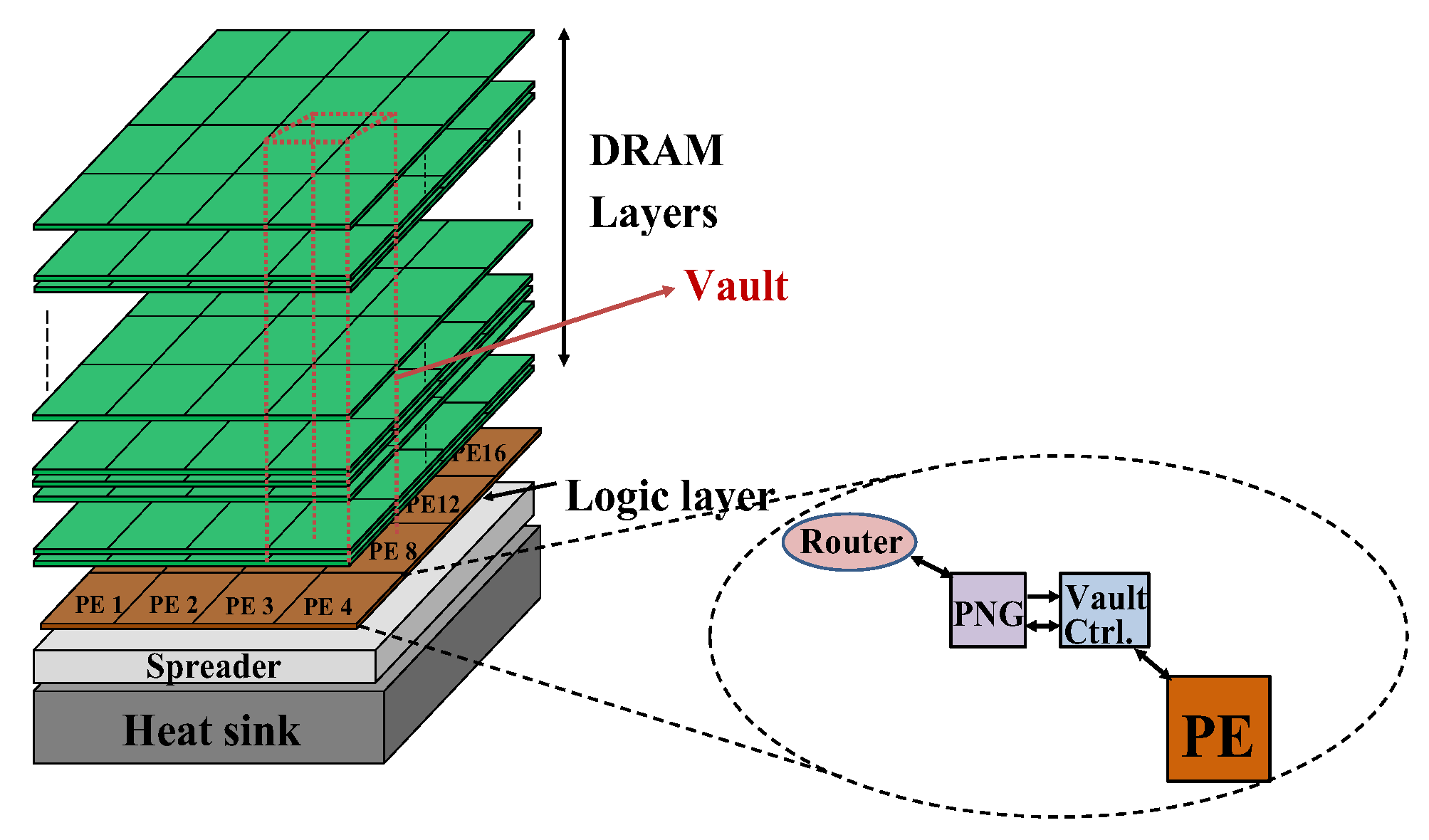
In our previous work [24], we set out an architecture to achieve efficient processing of neural networks through neuromorphic processing. The NeuroTower is effectively a 2D, mesh connected network-on-chip integrated with stacks of DRAM integrated on top for 3D stacked memory. This architecture employs programmable neurosequence generators, which act as a medium of communication in the system to aid with the retrieval of data between the DRAM stacks and processing elements. Our research introduces a pruning component to exploit sparsity and reduce network-on-chip traffic, a significant source of power consumption in many hardware accelerators. The pruning unit prevents ineffectual operations from being executed and leaves only the effectual data required for processing.
In NeuroTower, the memory is integrated as a stack of multiple DRAM chips each separated into 16 partitions. Along one column of partitions is a vault as shown in Figure 8 below. Each of these vaults has an associated vault controller which controls data movement in and out of the vaults to other elements of the NeuroTower. Each vault is connected to one processing element to allow for parallel processing and these connections are realized by using high speed through silicon vias (TSVs) [25]. The DRAM stack is crucial to the operation of the system as all the information for processing is contained here. Every layer of the neural network, their states, and connectivity weights are stored in the vaults of the DRAM. This implies that the data movement paths are known before beginning processing. To make use of this, the paths are compiled into finite state machine descriptions which drive the programmable neurosequence generators (PNG) [6]. To initiate processing the host must load these state machine descriptions into the PNG which begins the data-driven processing of each layer of the neural network.

7. Conclusions

With further advancements in neuromorphic computing which include large-scale implementations and on-chip learning, they have the potential to replace current Von-Neumann computers for running complex algorithms. Their power efficiency and learning capabilities allow them to drastically enhance the performance of a system. Future research needs to be completed regarding optimizing neuromorphic chip properties and learning techniques and using them for a wide range of applications, rather than only one specified application. Adopting a digital or mixed-design hardware approach for running complex AI algorithms with a NeuroTower architecture coupled with quantum computing can result in a flexible computing system with large memory, enhanced performance and speed, while reducing energy consumption.

Funding

This research received no external funding.

Data Availability Statement

Not Applicable.

Conflicts of Interest

The authors declare no conflicts of interest.

References

  1. Luo, T.; Wong, W.-F.; Goh, R.S.M.; Do, A.T.; Chen, Z.; Li, H.; Jiang, W.; Yau, W. Achieving Green AI with Energy-Efficient Deep Learning Using Neuromorphic Computing. Commun. ACM 2023, 66, 52–57. [Google Scholar] [CrossRef]
  2. Kumar, S.; Wang, X.; Strachan, J.P.; Yang, Y.; Lu, W.D. Dynamical memristors for higher-complexity neuromorphic computing. Nat. Rev. Mater. 2022, 7, 575–591. [Google Scholar] [CrossRef]
  3. Xu, B.; Huang, Y.; Fang, Y.; Wang, Z.; Yu, S.; Xu, R. Recent Progress of Neuromorphic Computing Based on Silicon Photonics: Electronic–Photonic Co-Design, Device, and Architecture. Photonics 2022, 9, 698. [Google Scholar] [CrossRef]
  4. Schuman, C.D.; Kulkarni, S.R.; Parsa, M.; Mitchell, J.P.; Date, P.; Kay, B. Opportunities for neuromorphic computing algorithms and applications. Nat. Comput. Sci. 2022, 2, 10–19. [Google Scholar] [CrossRef] [PubMed]
  5. Byun, K.; Choi, I.; Kwon, S.; Kim, Y.; Kang, D.; Cho, Y.W.; Yoon, S.K.; Kim, S. Recent Advances in Synaptic Nonvolatile Memory Devices and Compensating Architectural and Algorithmic Methods Toward Fully Integrated Neuromorphic Chips. Adv. Mater. Technol. 2022, 8. [Google Scholar] [CrossRef]
  6. Javanshir, A.; Nguyen, T.T.; Mahmud, M.A.P.; Kouzani, A.Z. Advancements in Algorithms and Neuromorphic Hardware for Spiking Neural Networks. Neural Comput. 2022, 34, 1289–1328. [Google Scholar] [CrossRef] [PubMed]
  7. Ivanov, D.; Chezhegov, A.; Kiselev, M.; Grunin, A.; Larionov, D. Neuromorphic artificial intelligence systems. Front. Neurosci. 2022, 16, 959626. [Google Scholar] [CrossRef] [PubMed]
  8. Shrestha, A.; Fang, H.; Mei, Z.; Rider, D.P.; Wu, Q.; Qiu, Q. A Survey on Neuromorphic Computing: Models and Hardware. IEEE Circuits Syst. Mag. 2022, 22, 6–35. [Google Scholar] [CrossRef]
  9. Wei, Q.; Gao, B.; Tang, J.; Qian, H.; Wu, H. Emerging Memory-Based Chip Development for Neuromorphic Computing: Status, Challenges, and Perspectives. IEEE Electron Devices Mag. 2023, 1, 33–49. [Google Scholar] [CrossRef]
  10. Guo, T.; Pan, K.; Jiao, Y.; Sun, B.; Du, C.; Mills, J.P.; Chen, Z.; Zhao, X.; Wei, L.; Zhou, Y.N.; et al. Versatile memristor for memory and neuromorphic computing. Nanoscale Horizons 2022, 7, 299–310. [Google Scholar] [CrossRef]
  11. Zhu, Y.; Mao, H.; Zhu, Y.; Wang, X.; Fu, C.; Ke, S.; Wan, C.; Wan, Q. CMOS-compatible neuromorphic devices for neuromorphic perception and computing: a review. Int. J. Extreme Manuf. 2023, 5, 042010. [Google Scholar] [CrossRef]
  12. B. Li, D. Zhong, X. Chen, and C. Liu, “Enabling Neuromorphic Computing for Artificial Intelligence with Hardware-Software Co-Design,” Artificial intelligence, Nov. 2023. [CrossRef]
  13. Christensen, D.V.; Dittmann, R.; Linares-Barranco, B.; Sebastian, A.; Le Gallo, M.; Redaelli, A.; Slesazeck, S.; Mikolajick, T.; Spiga, S.; Menzel, S.; et al. 2022 roadmap on neuromorphic computing and engineering. Neuromorphic Comput. Eng. 2022, 2, 022501. [Google Scholar] [CrossRef]
  14. Pham, M.D.; D’angiulli, A.; Dehnavi, M.M.; Chhabra, R. From Brain Models to Robotic Embodied Cognition: How Does Biological Plausibility Inform Neuromorphic Systems? Brain Sci. 2023, 13, 1316. [Google Scholar] [CrossRef]
  15. Zhang, H.; Ho, N.-M.; Polat, D.Y.; Chen, P.; Wahib, M.; Nguyen, T.T.; Meng, J.; Goh, R.S.M.; Matsuoka, S.; Luo, T.; et al. Simeuro: A Hybrid CPU-GPU Parallel Simulator for Neuromorphic Computing Chips. IEEE Trans. Parallel Distrib. Syst. 2023, 34, 2767–2782. [Google Scholar] [CrossRef]
  16. Das, R.; Biswas, C.; Majumder, S. Study of Spiking Neural Network Architecture for Neuromorphic Computing. 2022 IEEE 11th International Conference on Communication Systems and Network Technologies (CSNT), Apr. 2022. [Google Scholar] [CrossRef]
  17. Spyrou, T.; Stratigopoulos, H.-G. On-Line Testing of Neuromorphic Hardware. May 2023. [CrossRef]
  18. Frenkel, C.; Bol, D.; Indiveri, G. Bottom-Up and Top-Down Approaches for the Design of Neuromorphic Processing Systems: Tradeoffs and Synergies Between Natural and Artificial Intelligence. Proc. IEEE 2023, 111, 623–652. [Google Scholar] [CrossRef]
  19. Clark, K.; Wu, Y. Survey of Neuromorphic Computing: A Data Science Perspective. May 2023. [CrossRef]
  20. Garg, N.; Balafrej, I.; Stewart, T.C.; Portal, J.-M.; Bocquet, M.; Querlioz, D.; Drouin, D.; Rouat, J.; Beilliard, Y.; Alibart, F. Voltage-dependent synaptic plasticity: Unsupervised probabilistic Hebbian plasticity rule based on neurons membrane potential. Front. Neurosci. 2022, 16, 983950. [Google Scholar] [CrossRef] [PubMed]
  21. Wunderlich, T.; Kungl, A.F.; Müller, E.; Hartel, A.; Stradmann, Y.; Aamir, S.A.; Grübl, A.; Heimbrecht, A.; Schreiber, K.; Stöckel, D.; et al. Demonstrating Advantages of Neuromorphic Computation: A Pilot Study. Front. Neurosci. 2019, 13, 260. [Google Scholar] [CrossRef]
  22. Ghosh, S.; Nakajima, K.; Krisnanda, T.; Fujii, K.; Liew, T.C.H. Quantum Neuromorphic Computing with Reservoir Computing Networks. Adv. Quantum Technol. 2021, 4, 2100053. [Google Scholar] [CrossRef]
  23. Hoffmann, A.; Ramanathan, S.; Grollier, J.; Kent, A.D.; Rozenberg, M.J.; Schuller, I.K.; Shpyrko, O.G.; Dynes, R.C.; Fainman, Y.; Frano, A.; et al. Quantum materials for energy-efficient neuromorphic computing: Opportunities and challenges. APL Mater. 2022, 10, 070904. [Google Scholar] [CrossRef]
  24. Asad and, F. Mohammadi, “NeuroTower: A 3D Neuromorphic Architecture with Low-Power TSVs,” Lecture notes in networks and systems, pp. 227–236, Oct. 2022. [CrossRef]
  25. Panzeri, S.; Janotte, E.; Pequeño-Zurro, A.; Bonato, J.; Bartolozzi, C. Constraints on the design of neuromorphic circuits set by the properties of neural population codes. Neuromorphic Comput. Eng. 2023, 3, 012001. [Google Scholar] [CrossRef]
  26. Bartolozzi, C.; Indiveri, G.; Donati, E. Embodied neuromorphic intelligence. Nat. Commun. 2022, 13, 1–14. [Google Scholar] [CrossRef]
  27. Zhong, Y.; Wang, Z.; Cui, X.; Cao, J.; Wang, Y. An Efficient Neuromorphic Implementation of Temporal Coding-Based On-Chip STDP Learning. IEEE Trans. Circuits Syst. II: Express Briefs 2023, 70, 4241–4245. [Google Scholar] [CrossRef]
  28. Kimura, M.; Shibayama, Y.; Nakashima, Y. Neuromorphic chip integrated with a large-scale integration circuit and amorphous-metal-oxide semiconductor thin-film synapse devices. Sci. Rep. 2022, 12, 1–6. [Google Scholar] [CrossRef]
  29. Asad, A.; Kaur, R.; Mohammadi, F. A Survey on Memory Subsystems for Deep Neural Network Accelerators. Futur. Internet 2022, 14, 146. [Google Scholar] [CrossRef]
  30. R. Kaur, A. Asad, and F. Mohammadi, “A Comprehensive Review on Processing-in-Memory Architectures for Deep Neural Networks,” Jun. 2024. [CrossRef]
Figure 1. Four main spiking neuron models used in neuromorphic chips.
Preprints 110779 g001
Figure 2. Neuromorphic architecture characterization diagram.
Preprints 110779 g002
Figure 3. Neuromorphic computing learning methods characterization diagram.
Preprints 110779 g003
Figure 4. Von Neumann architecture versus Neuromorphic architecture.
Preprints 110779 g004
Figure 5. Example of SNN and information transmission between neurons through synapses.
Preprints 110779 g005
Figure 6. Backpropagation algorithm network structure [4].
Preprints 110779 g006
Figure 7. Spike-timing dependent plasticity architecture where the weights are adjusted based on the spike timings of the pre-synaptic neurons (i) and post-synaptic neurons (j) [4].
Preprints 110779 g007
Figure 8. NeuroTower architecture with depiction of stacked memory.
Preprints 110779 g008
Table 1. Summary of neuromorphic project properties [7].
Property TrueNorth Loihi
In-memory Computation Near-memory Near-memory
Signal Spikes Spikes
Size neurons/synapses 1M/256M 128K/128M
On-device learning No STDP
Analog No No
Event-based Yes Yes
nm 28 14
Features First industrial neuromorphic chip without training (IBM) First neuromorphic chip with training (Intel)
Property Loihi2 Tianjic
In-memory Computation Near-memory Near-memory
Signal Real numbers, Spikes Real numbers, Spikes
Size neurons/synapses 120K/1M 40K/10M
On-device learning STDP No
Analog No No
Event-based Yes Yes
nm 7 28
Features Non-binary spikes, neurons can be programmed Hybrid chip
Property SpiNNaker Brain-ScaleS
In-memory Computation Near-memory Yes
Signal Real numbers, Spikes Real numbers, Spikes
Size neurons/synapses - 512/130K
On-device learning STDP STDP
Analog No Yes
Event-based No Yes
nm 22 65
Features Scalable computer for SNN simulation Analog neurons, large size
Property GrAIOne Akida
In-memory Computation Near-memory Near-memory
Signal Real numbers, Spikes Spikes
Size neurons/synapses 200K/- 1.2M/10B
On-device learning No STDP
Analog No No
Event-based Yes Yes
nm 28 28
Features NeuronFlow architecture, effective support of sparse computations Incremental, one-shot and continuous learning for CNN
Property Memristor (IBM)
In-memory Computation Yes
Signal Spikes
Size neurons/synapses 512/64K
On-device learning Yes
Analog Yes
Event-based Yes
nm 50
Features Allows each synaptic cell to operate asynchronously
Disclaimer/Publisher’s Note: The statements, opinions and data contained in all publications are solely those of the individual author(s) and contributor(s) and not of MDPI and/or the editor(s). MDPI and/or the editor(s) disclaim responsibility for any injury to people or property resulting from any ideas, methods, instructions or products referred to in the content.
Copyright: This open access article is published under a Creative Commons CC BY 4.0 license, which permit the free download, distribution, and reuse, provided that the author and preprint are cited in any reuse.
Prerpints.org logo

Preprints.org is a free preprint server supported by MDPI in Basel, Switzerland.

Subscribe

© 2024 MDPI (Basel, Switzerland) unless otherwise stated