Preprint
Article

Current-Mode Control of a Distributed Buck Converter with a Lossy Transmission Line

This version is not peer-reviewed.

Submitted:

02 July 2024

Posted:

03 July 2024

You are already at the latest version

A peer-reviewed article of this preprint also exists.

Abstract
This article presents a buck converter in which the inductor has been replaced by a transmission line. This approach would be practically conceivable if the power supply and load have a greater spatial distance. In the time domain, this new converter can be described by a system of coupled partial and ordinary differential equations. In the frequency domain, a transcendental transfer function is obtained. For comparison with an equivalently parameterized conventional converter, Padé approximants are derived. A linear controller is designed for the converter topology under consideration.
Keywords: 
Subject: 
Engineering  -   Electrical and Electronic Engineering

1. Introduction

Switched-mode power supply became increasingly popular in the last decades. The applications range from small electronic devices to the electrical power grid. In the field of home electronics and mobile devices, switched-mode DC/DC converters have almost completely replaced the linear regulators that were previously used.
Like other power supplies, switched-mode converters transfer power from a source to a load. In many cases, a desired output voltage must be set, but other targets such as current or power could also be specified. A buck converter (step-down converter) is used to provide a lower output voltage, while a boost (step-up converter) converter would be used to provide a higher output voltage. Certain converter types, such as buck-boost converters or Ćuk converters, are able to provide both lower and higher output voltages [1].
Switched-mode DC/DC converters store the energy from the power supply temporarily in reactive network elements, i.e., inductors and capacitors, and then release that energy to the load at a different voltage. The largest and most material-intensive component of the converter is typically the inductor, i.e., the choke. In [2,3,4], the power inductor was replaced by a transmission line resulting in distributed converter models. In [5,6,7], both the inductor and the capacitor were replaced by a transmission line. In other publications, the connection of conventional switched-mode converter circuits (i.e., with discrete reactive elements) to the load via transmission lines is investigated [8,9].
In the work [2,3], mathematical models were first derived for some converter circuits with transmission line. This was followed by a spatial discretization of this transmission line. The approach leads to a lumped model in which the power inductor is replaced by several smaller coils and capacitors. The motivation for [4,6,7] was different. If the power supply and the load are physically separated, wired energy transmission is unavoidable. The idea behind the work was to replace reactive network elements with this supply line, which was needed anyway. In the buck converter, the transmission line can in principle replace both the inductor and the capacitor. In the boost converter, the switch is located between the two elements so that the transmission line can only replace the coil. An experimental verification of these concepts with practical implementations was carried out in [2,3] as well as in [6,7].
The modeling of conventional converter circuits initially leads to differential algebraic equations that can be reduced to ordinary differential equations [1]. After linearization, if necessary, a rational transfer function is obtained in the frequency domain. The modeling of a transmission line leads to partial differential equations which, if further discrete reactive network elements are present, have to be combined with ordinary differential equations [10,11]. In the frequency domain, this results in a transcendental transfer function, which typically contains exponential or hyperbolic functions.
Numerous control concepts have been investigated for conventional converter circuits, both linear and nonlinear, e.g. [1,12,13,14]. In practical applications, linear controllers are dominant [1,15,16]. Controller design for the class of distributed converter models, i.e., converters with a transmission line, is significantly more challenging due to the different type of mathematical models, e.g. see [17,18,19].
In this paper we investigate a modified buck converter, where the inductor is replaced by a transmission line. Unlike the previous work [5,6,7], the transmission line does not replace the capacitor. This approach leads to a significantly lower first resonance frequency compared to the previous work. The modified buck converter is also considered in the frequency domain. For this model, a transcendental transfer function is derived and its rational approximations are discussed. In addition, we design a linear controller based on the conventional converter model with equivalent parameters.
The paper is structured as follows: In Section 2 we derive mathematical models for the conventional and the distributed buck converter in the time as well as the frequency domain. The transient simulation of these converter models in discussed in Section 3. The description in the frequency domain and the behavior of the models under periodic excitation is investigated in Section 4. In Section 5 we present the controller design and simulate the closed loop control system. Our results are discussed in Section 6.

2. Buck Converter Modeling

2.1. Lumped Parameter Model of the Standard Buck Converter

The circuit diagram of a standard buck converter is shown in Figure 1 (left). The buck converter is a switched-mode power supply designed to reduce an input voltage to a lower output voltage. The switching is often carried out by a transistor in combination with a freewheeling diode. This topology is known as an asynchronous buck converter. In our circuit diagram, we show an insulated-gate bipolar transistor (IGBT), but one could also use a bipolar junction transistors (BJT) or a metal–oxide–semiconductor field-effect transistor (MOSFET). Sometimes the diode is replaced by a second transistor resulting in a synchronous buck converter. Furthermore, the converter consists of a coil (choke) and a capacitor. In this paper, the converter feeds a resistive load.
From the schematics we derive the network model shown in Figure 1 (right). The supply voltage E is considered as an ideal constant voltage source. The semiconductor circuitry is modeled as a single pole changeover switch with the two positions d = 0 and d = 1 . The coil is described by an inductance L with conductor resistance  R L . The capacitor is modeled by a capacity C with an insulation conductance  G C . The load is ohmic with a resistance R.
From the network model we obtain the ordinary differential equations (ODEs)
L d i ( t ) d t + R L i ( t ) + v ( t ) = E d ( t )
C d v ( t ) d t + G C + 1 R v ( t ) = i ( t )
with L , C , R > 0 and R L , G C 0 . These ODEs constitute a lumped parameter model in the time domain [20]. The ODEs can be transformed from the time to the frequency domain using the Laplace transform
s L + R L 1 1 s C + G C + 1 R M ( s ) I ( s ) V ( s ) = E 0 D ( s ) ,
where we use capital letters for the transformed signals and assumed vanishing initial values, i.e., i ( 0 ) = 0 and v ( 0 ) = 0 . For current-mode control we use (3) to derive the transfer function
P ( s ) = I ( s ) D ( s ) = E s C + G C + 1 R L C s 2 + L G C + R L C + L R s + 1 + R L G C + 1 R
from the switching signal  D ( s ) to the current  I ( s ) . This second order transfer function corresponds to a damped harmonic oscillator. The stability property holds even in the case of lossless reactive network elements (i.e., R L = 0 and G C = 0 ) due to the damping resulting from the load resistance  R > 0 .

2.2. Distributed Parameter Model of the Buck Converter with Lossy Transmission Line

If there is a certain spatial distance between the voltage source and the load, then the electrical energy transmission could be described by a transmission line. This transmission line could also be used to replace the inductor. The second reactive element of the converter circuit, the capacitor, is present as a discrete component in parallel with the load. Replacing only one reactive element with the transmission line corresponds to the approach described in [2,3,4]. The circuit topology of the resulting converter is shown in Figure 2.
Central part of the new converter topology is the transmission line, which can be modeled by the partial differential equations
L t i ( z , t ) + R L i ( z , t ) + z v ( z , t ) = 0 ,
C t v ( z , t ) + G C v ( z , t ) + z i ( z , t ) = 0
known as telegrapher’s equations [10,11]. The current i and the voltage u along the transmission line depend both on the time  t 0 and the spatial position z [ 0 , l ] , where l denotes the length of the transmission line. The parameters L , C , R L , G C describe inductance, capacitance, resistance and conductance per length, respectively. These PDEs constitute a distributed parameter model [20].
Both ends of the transmission line are connected to the remaining circuitry. Mathematically, these connections are described by boundary conditions. On the left hand side, i.e., at z = 0 , we have the input voltage E d ( t ) resulting from the voltage source and the switch. On the right hand side, i.e., at z = l , we have the parallel circuit of the external capacitor  C ext > 0 and the ohmic load  R > 0 . This leads to the Robin boundary conditions
v ( 0 , t ) = E d ( t )
C ext v ˙ ( l , t ) + 1 R v ( l , t ) = i ( l , t )
because the second condition is specified by a linear combination of the voltage and it time derivative on the spatial boundary. Therefore, we can consider the overall model (5)-(8) as a coupled PDE-ODE system.
For further investigations we transform the PDE (5) and (6) from the time into the Laplace frequency domain
( s L + R L ) I ( z , s ) + z V ( z , s ) = 0 ,
( s C + G C ) V ( z , s ) + z I ( z , s ) = 0 ,
where the spatial dependency remains unchanged. Similar as in Section 2.1 we assume vanishing initial values, i.e., i ( · , 0 ) = 0 and v ( · , 0 ) = 0 . We can rewrite (9) and (10) as a linear state-space model
z I ( z , s ) V ( z , s ) = 0 ( s C + G C ) ( s L + R L ) 0 A ( s ) I ( z , s ) V ( z , s ) X ( z , s )
where the ODEs are formulated in terms of the spatial variable z. The characteristic equation
det γ I A ( s ) = γ 2 ( s L + R L ) ( s C + G C ) = 0 ,
where I denotes the identity matrix, has the roots
γ 1 , 2 ( s ) = ± s L + R L s C + G C .
In general, the solution of an initial value problem of the linear system (11) can be written as
X ( z , s ) = exp ( A ( s ) z ) X ( 0 , s )
with the matrix exponential function
exp ( A ( s ) z ) = k = 0 1 k ! A ( s ) z k .
Using the linear dependency
A ( s ) 2 = s L + R L s C + G C I = γ 2 I ,
we can decompose the series expansion (14) into odd and even terms and obtain
exp ( A ( s ) z ) = cosh ( γ z ) I + 1 γ sinh ( γ z ) A .
For current-mode controller design, we want to describe the input output relation on the left boundary (7) taking the right boundary condition (8) into account. In the Laplace domain, condition (8) can be written as
V ( l , s ) = Z ( s ) I ( l , s ) with Z ( s ) = R 1 s C ext = R 1 + s R C ext ,
where the impedance Z describes the parallel connection of R and C ext . To describe the conditions on the left boundary, we solve (13) w.r.t. the initial vector
X ( 0 , s ) = exp ( A ( s ) l ) X ( l , s )
and set z = l for the right boundary. The exponential matrix (14) is always invertible. In (17), the inverse exponential matrix results from the reverse spatial direction. Using (15) we have
M ( s ) : = exp ( A ( s ) l ) = cosh ( γ l ) I 1 γ sinh ( γ l ) A ( s ) = cosh ( γ l ) 1 γ ( s C + G L ) sinh ( γ l ) 1 γ ( s L + R L ) sinh ( γ l ) cosh ( γ l ) .
With M = ( m i j ) we can write (17) element-wise as
I ( 0 , s ) = m 11 ( s ) I ( l , s ) + m 12 ( s ) V ( l , s ) = m 11 ( s ) + m 12 ( s ) Z ( s ) I ( l , s )
and
V ( 0 , s ) = m 21 ( s ) I ( l , s ) + m 22 ( s ) V ( l , s ) = m 21 ( s ) + m 22 ( s ) Z ( s ) I ( l , s ) .
Combining (7), (18) and (19) we obtain the transfer function
P ( s ) = I ( 0 , s ) D ( s ) = I ( 0 , s ) V ( 0 , s ) E = m 11 ( s ) + m 12 ( s ) Z ( s ) m 21 ( s ) + m 22 ( s ) Z ( s ) E = s C + G C Z ( s ) sinh ( γ l ) + γ cosh ( γ l ) s L + R L sinh ( γ l ) + γ Z ( s ) cosh ( γ l ) E = s C + G C R sinh ( γ l ) + γ 1 + s R C ext cosh ( γ l ) s L + R L 1 + s R C ext sinh ( γ l ) + γ R cosh ( γ l ) E
from the duty ratio to the current into the transmission line.

3. Simulation Models

3.1. Model Parameters

In this paper, we want to investigate a new converter topology and compare it with the standard buck converter. For this reason, the parameters for the distributed parameter converter are determined first. The parameters of the lumped parameter converter are then determined in an equivalent manner for a suitable comparison.
Central part of the new buck converter is the transmission line. In this paper we consider the transmission line, which was used in practical realizations discussed in [6,7]. In particular, we use l = 6 m coaxial cable RG 58 C/U [21]. The inductance and capacitance per length are L = 241 n H / m and C = 100 p F / m , respectively. While a lossless cable was considered in [6,7], the losses are taken into account in this publication. According to [22], the coaxial cable RG 58 C/U has a maximum conductor resistance of 40.7 Ω / k m . For our considerations we assume R L = 40 Ω / k m = 40 m Ω / m . Furthermore, the minimum insulation resistance is 5 G Ω × k m resulting in the conductance per length of G C = 0.2 p S / m . These primary line constants result in the following integral values of the transmission line:
L ¯ = l · L = 1446 n H , C ¯ = l · C = 600 p F , R ¯ L = l · R L = 240 m Ω , G ¯ C = l · G C = 1.2 p S .
In addition to the transmission line, the new converter possesses an external capacitor with the capacitance C ext = 1 μ F . In connection with (21) we define the following parameter values for the standard buck converter:
L = L ¯ = 1446 n H , C = C ¯ + C ext = 1000.6 n F , R L = R ¯ L = 240 m Ω , G C = G ¯ C = 1.2 p S .
Both converters are supplied with  E = 12 V and operated with the load R = 10 Ω .

3.2. State-Space Model of the Standard Buck Converter

We can rewrite the network equations (1) and (2) as a two-dimensional state-space model
x ˙ ( t ) = A x ( t ) + B d ( t ) , y ( t ) = C x ( t ) + D d ( t ) .
With the state vector x = ( x 1 , x 2 ) T = ( i , v ) T , the system matrix A R 2 × 2 , the input matrix B R 2 × 1 , the output matrix C R 2 × 2 and the throughput matrix D R 2 × 1 are given by
A = R L L 1 L 1 C 1 + R G C R C , B = E L 0 , C = 1 0 0 1 , D = 0 0
with the parameters listed in (22). The output matrix is a 2 × 2 identity matrix such that both components of the state vector are available on the output for measurement. The throughput matrix is a zero matrix because the system doesn’t have a direct throughput. Therefore, the output vector has the form
y ( t ) = x ( t ) = i ( t ) v ( t ) .
Consider a constant input signal d 0 [ 0 , 1 ] . For a non-singular system matrix  A the state-space model (23) has an unique equilibrium point at
x 0 = A 1 B d 0 .
With the matrices (24) we obtain
x 0 = i 0 v 0 = G C R + 1 E G C R R L + R + R L d 0 E R G C R R L + R + R L d 0 .
From R , R L , G C > 0 we conclude 0 v 0 < E , i.e., the voltage in the equilibrium point is always less than the supply voltage E.
By (25) the current and the voltage in the equilibrium point are specified by the input values  d 0 . In practice, a desired voltage is usually specified. For a prescribed reference v 0 , the values of the reference current and the reference input are given by
i 0 = G C R + 1 R v 0 and d 0 = G C R + 1 R L + R E R v 0 .

3.3. State-Space Model of the Buck Converter with Transmission Line
To simulate the distributed converter, the transmission line is replaced by a spatially discretized network model. Figure 3 shows the resulting network model, where the integer N is the number of spatial discretization steps. The parameters δ L , δ R L and δ C , δ G C describe the inductance and the conductor resistance as well as the capacitance and insulation conductance per discretized element, respectively.
Kirchhoff’s voltage law result in the network equations
δ L d d t i 1 ( t ) + δ R L i 1 ( t ) = d ( t ) E v 1 ( t ) , δ L d d t i 2 ( t ) + δ R L i 2 ( t ) = v 1 ( t ) v 2 ( t ) , δ L d d t i N 1 ( t ) + δ R L i N 1 ( t ) = v N 2 ( t ) v N 1 ( t ) , δ L d d t i N ( t ) + δ R L i N ( t ) = v N 1 ( t ) v N ( t ) ,
and Kirchhoff’s current law yields the further network equations
δ C v ˙ 1 ( t ) + δ G C v 1 ( t ) = i 1 ( t ) i 2 ( t ) , δ C v ˙ 2 ( t ) + δ G C v 2 ( t ) = i 2 ( t ) i 3 ( t ) , δ C v ˙ N 1 ( t ) + δ G C v N 1 ( t ) = i N 1 ( t ) i N ( t ) , δ C + C ext v ˙ N ( t ) + δ G C + 1 R v N ( t ) = i N ( t ) .
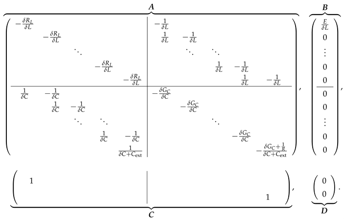
These equations can be written as a state-space system (23). Defining the state vector
x = i 1 i 2 i N 1 i N v 1 v 2 v N 1 v N T
we obtain the matrices A R 2 N × 2 N , B R 2 N × 1 , C R 2 × 2 N and D R 2 × 1 of the form
Preprints 111065 i001
The simulation model has two outputs. We use the the first current and the last voltage of the discretized model (27) and (28). Again, the throughput matrix is a zero matrix because the system doesn’t have a direct throughput. Hence, we have the output vector
y ( t ) = i 1 ( t ) u N ( t ) .
In our simulation we use N = 25 . This results in the following parameters in the system matrices (29) of the discretized model:
δ L = L ¯ / N = 57.84 n H , δ C = C ¯ / N = 24 p F , δ R L = R ¯ L / N = 9.6 m Ω , δ G L = G ¯ C / N = 0.048 p S .

3.4. Open Loop Transient Simulation

In this section we will carry out open loop transient simulations of the converter models derived in Section 3.2 and Section 3.3. For the numerical simulation we employ Scilab 2024 [23] with the graphical editor Xcos under Fedora Linux 39.
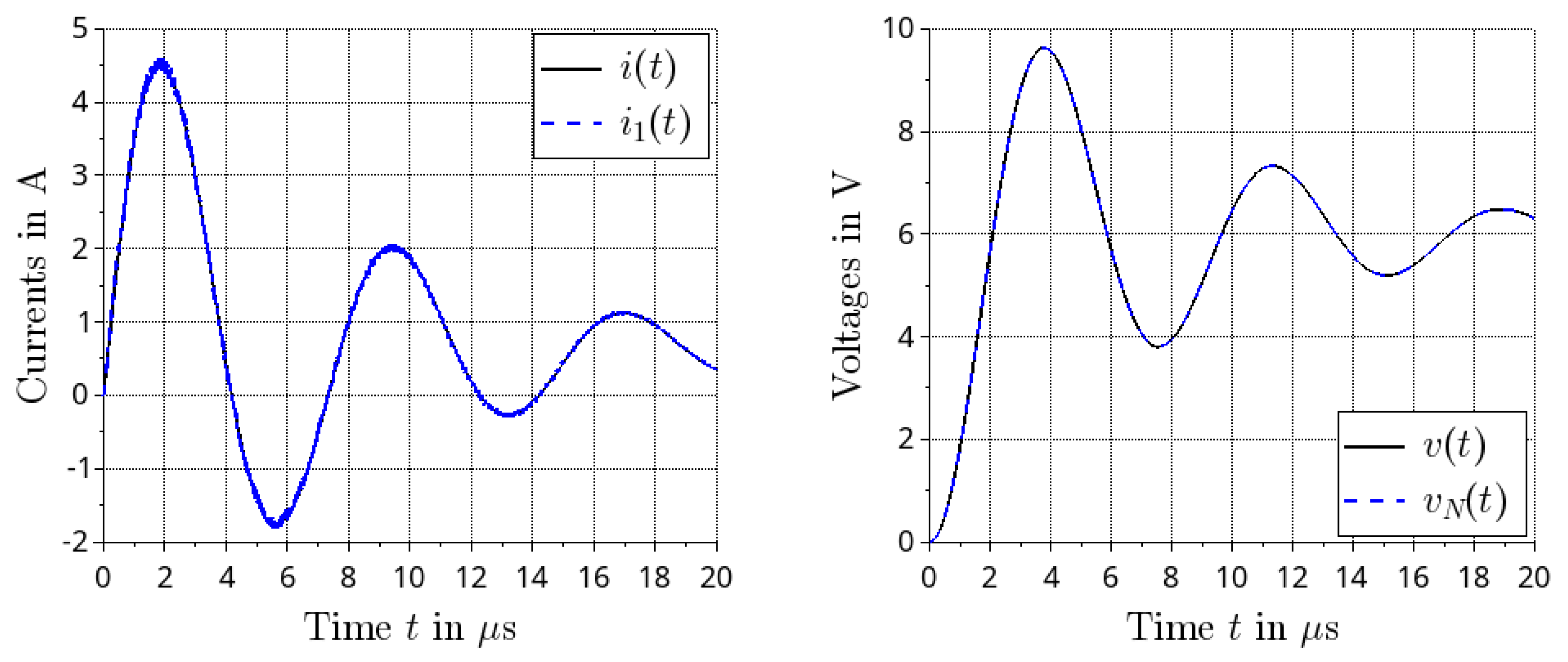
Using the parameters given in Section 3.1 and taking the losses described by  R L and  G C into account, the largest output voltage that can be achieved continuously is v 0 11.72 V resulting from (25) with d 0 = 1 . In our considerations, the buck converter should be operated in such a way that an output voltage of v 0 = 6 V is produced. With (26) we obtain the reference input d 0 0.512 . With this constant input signal, the current i 0 0.6 A should be achieved asymptotically. For both converter models we used a zero vector of appropriate dimension as an initial value. Figure 4 shows the simulation results. The step response of the classic converter corresponds to a stable second-order oscillatory system due to its overshoot. The current of the discretized distributed converter oscillates with a higher frequency around the current of the standard buck converter as shown in Figure 4 (left). The output voltages of both converters match visually, see Figure 4 (right). The first voltage peak occurs at t 3.78 μ s , the second at t 11.345 μ s . Therefore, the declining oscillation has a period of approximately 11.345 μ s 3.78 μ s = 7.565 μ s , which corresponds to a frequency of roughly 1 / 7.565 μ s 132 k H z .
While any value of the input signal  d ( t ) can be applied to the linear continuous-time model (23), only discrete values d ( t ) { 0 , 1 } are possible with the converter circuit. A pulse width modulation (PWM) can be used to simulate continuous values in the interval d ( t ) [ 0 , 1 ] . In particular, for a given number D [ 0 , 1 ] the switching signal is generated by
d ( t ) = 1 if mod ( t , T PWM ) D T PWM 0 otherwise
with the switching time  T PWM > 0 and the switching frequency f PWM = 1 / T PWM . The number D is called duty ratio or duty cycle [1]. In an analog implementation, the switching signal would be generated using a sawtooth oscillation and a comparator as shown in Figure 5. In a digital implementation, counters are used.
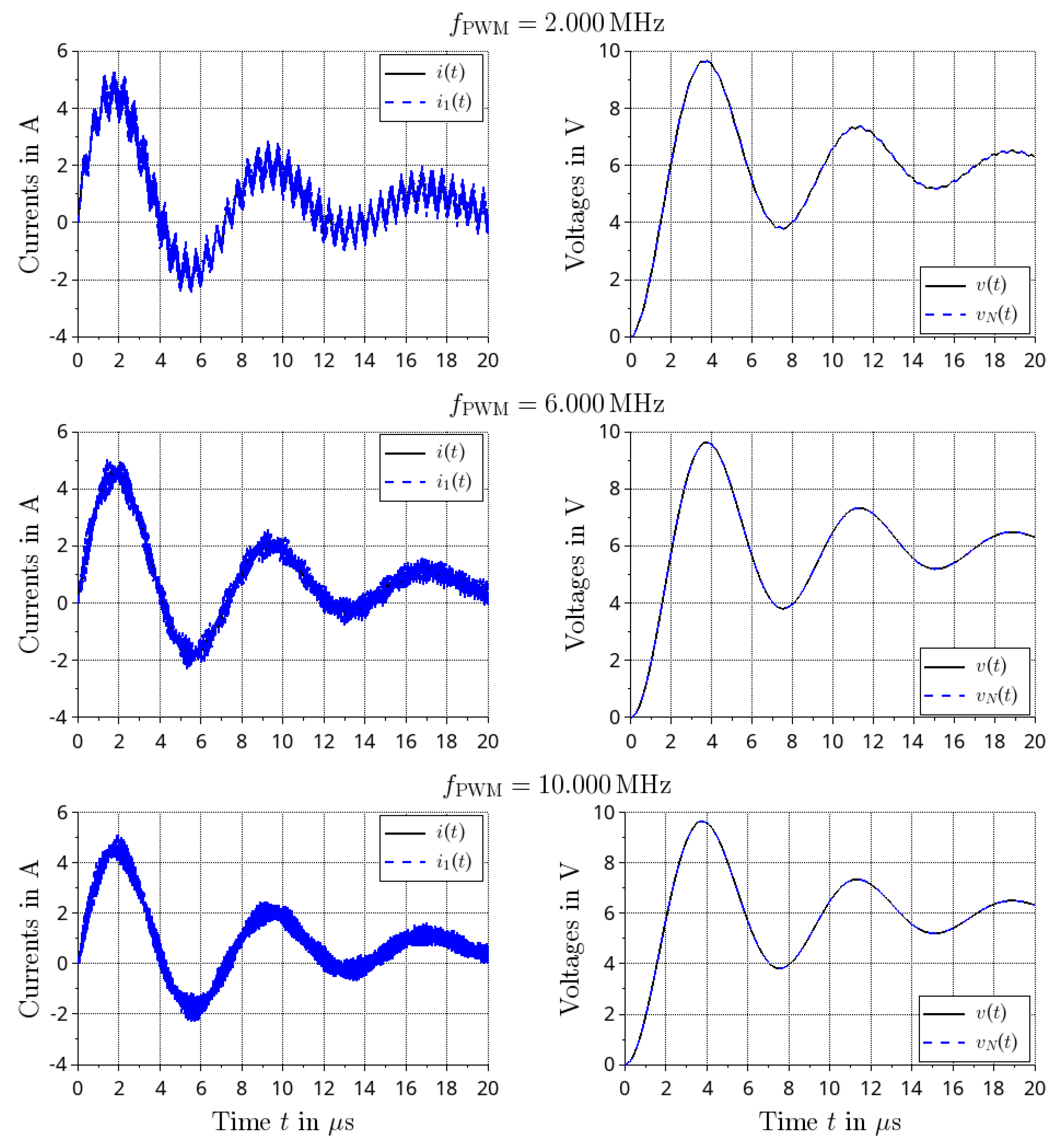
Next, we simulated both converters under PWM excitation. To achieve the desired output voltage v 0 = 6 V we used the duty ratio D = d 0 0.512 . The transient simulation results of the state-space models of the standard and the discretized distributed buck converter are shown in Figure 6. As initial vectors we used zero vectors of appropriate dimensions. The simulations were carried out for different PWM frequencies f PWM { 2 M H z , 6 M H z , 10 M H z } . For the discretized distributed converter, there are significant current ripples due to traveling waves in the transmission line, which tend to decrease with increasing PWM frequency. On the other hand, the voltage ripples can just about be seen at f PWM = 2 M H z , but not at the higher frequencies used here. The voltage peaks are smoothed by the external capacitor. This represents a significant improvement compared to the investigations in [6,7].

4. Frequency Domain

4.1. Transfer Function

The input-output behavior of the classical buck converter is described by the transfer function (4). Using the parameter values given in Section 3.1 we obtain
P ( s ) = 8298755.186721992 s + 829377891946.9895 s 2 + 265915.1397140521 s + 707735801119.8038 .
The transfer function is strictly proper. The (normalized) poles s 1 , 2 132957.57 ± 830697.35 j are a conjugate pair located in the left half plane. The step response of (32) should result in a declining oscillation, which is consistent with the numerical simulation carried out in Section 3.4, see Figure 4.
The transfer function for the distributed converter was derived in (20). We omit printing this transfer function with the numerical parameter values because the corresponding expression is very large. However, this transfer function is not rational, but transcendent. This property complicates controller design because many design methods require a rational transfer function of the plant. To avoid these difficulties we will approximate the transcendent transfer function (20) by a rational function.
Given a transfer function P, the Padé approximant of order ( m , n ) is the rational function
P m , n ( s ) = b m s m + + b 1 s + b 0 s n + a n 1 s n 1 + + a 1 s + a 0 .
To obtain the Padé approximant (33) we expand the original function P in a Maclaurin series (i.e., a Taylor series at 0) with n + m coefficients:
P ( s ) = c 0 + c 1 s + + c n + m s n + m + O ( s n + m + 1 ) .
The coefficeints a 0 , , a n 1 , b 0 , , b m are calculated via coefficient matching between (33) and (34).
The Taylor expansion (34) required to calculate the Padé approximant (33) led to error messages in the computer algebra programs Maxima 5.45.1 [24] and SageMath 10.2 [25]. The issues with the series expansion most likely result from the term  γ , which is a square root according to (12). In the series expansion of the functions occurring in (15), however, the term  γ only occurs in even powers:
cosh ( γ z ) = 1 + 1 2 γ 2 z 2 + 1 24 γ 4 z 4 + , 1 γ sinh ( γ z ) = z + 1 6 γ 2 z 3 + 1 120 γ 4 z 5 + .
Note that these are entire functions in s. If you use these series expansions when calculating the transfer function (20), one can avoid the problems mentioned above as there is no longer a square root.
The RC element at the right boundary of the transmission line would tend to produce a low-pass behavior, at least for high frequencies. This qualitative assumption leads to the requirement m < n for the Padé approximant (33), i.e., to a strictly proper transfer function. With SageMath 10.2 [25] we computed the following low order Padé approximants
P 0 , 1 ( s ) = 121684.784841855 s 103837.683063803
P 1 , 2 ( s ) = 8.30398290026456 × 10 6 s + 8.29900199309498 × 10 11 s 2 + 265983.502353863 s + 7.08181503402271 × 10 11
of the transcendent transfer function (20).

4.2. Response under Sinusoidal Excitation

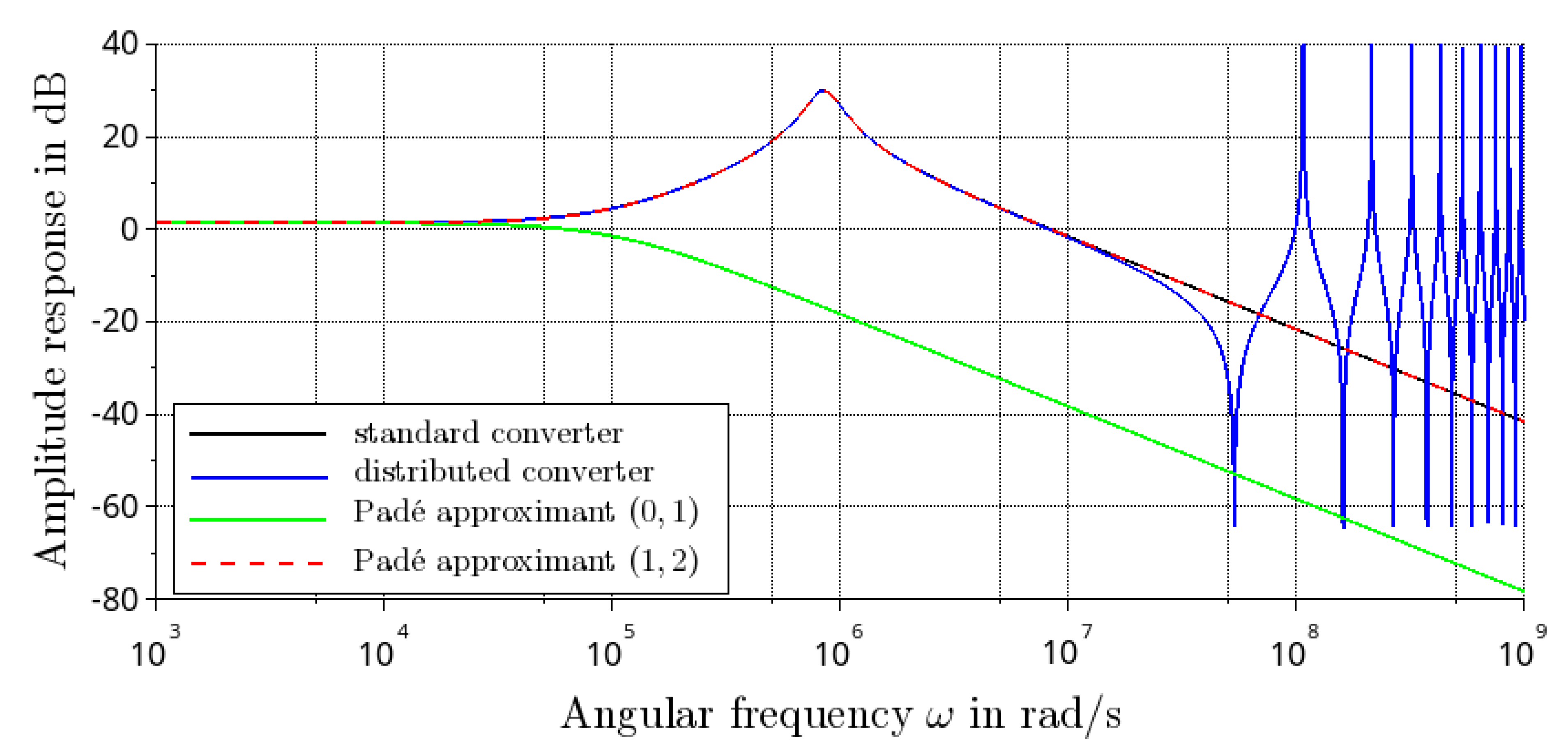
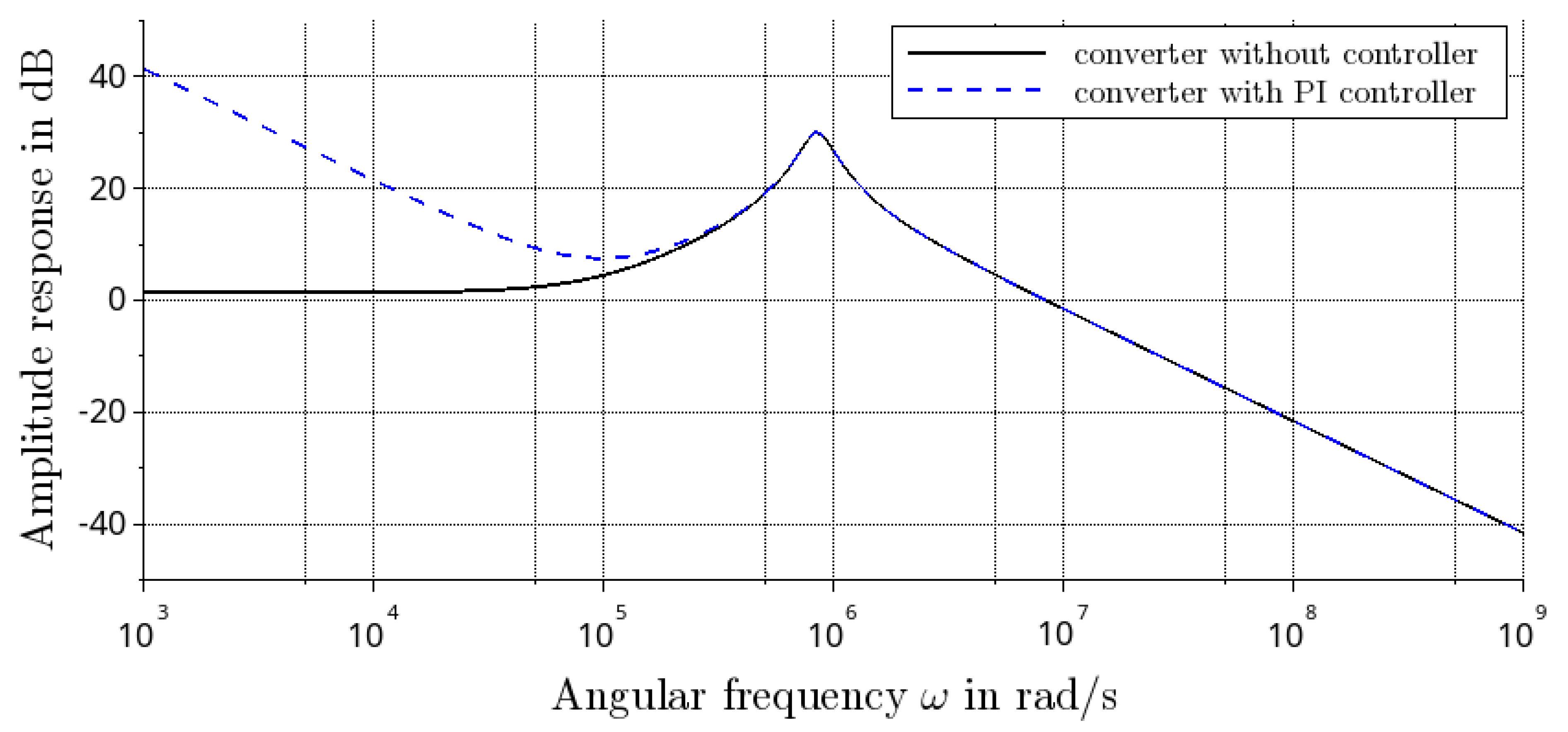
The amplitude frequency responses of derived transfer functions are shown in Figure 7. The amplitude responses of the classical and the distributed converter as well as its Padé approximant of order ( 1 , 2 ) agree up to ω 10 7 rad / s . The transcendent transfer function (20) of the distributed converter shows a qualitatively different behavior for ω 10 7 rad / s . These three models have a resonance peak with an angular resonance frequency ω 0 0.841 × 10 6 rad / s corresponding to the technical frequency f 0 = ω 0 / 2 π 134 k H z . This is consistent with the frequency of the declining oscillations observed in the transient simulation in Section 3.4. Of course, the resonance peak cannot be described by the Padé approximant of order ( 0 , 1 ) . In contrast, an antiresonance can only occur with the distributed converter model. The first angular antiresonance frequency occurring at ω 1 53.3 × 10 6 rad / s corresponds to the technical frequency f 1 = ω 1 / 2 π 8.49 M H z . With increasing frequencies, resonances and antiresonances alternate for the distributed converter model.

4.3. Response under PWM Excitation

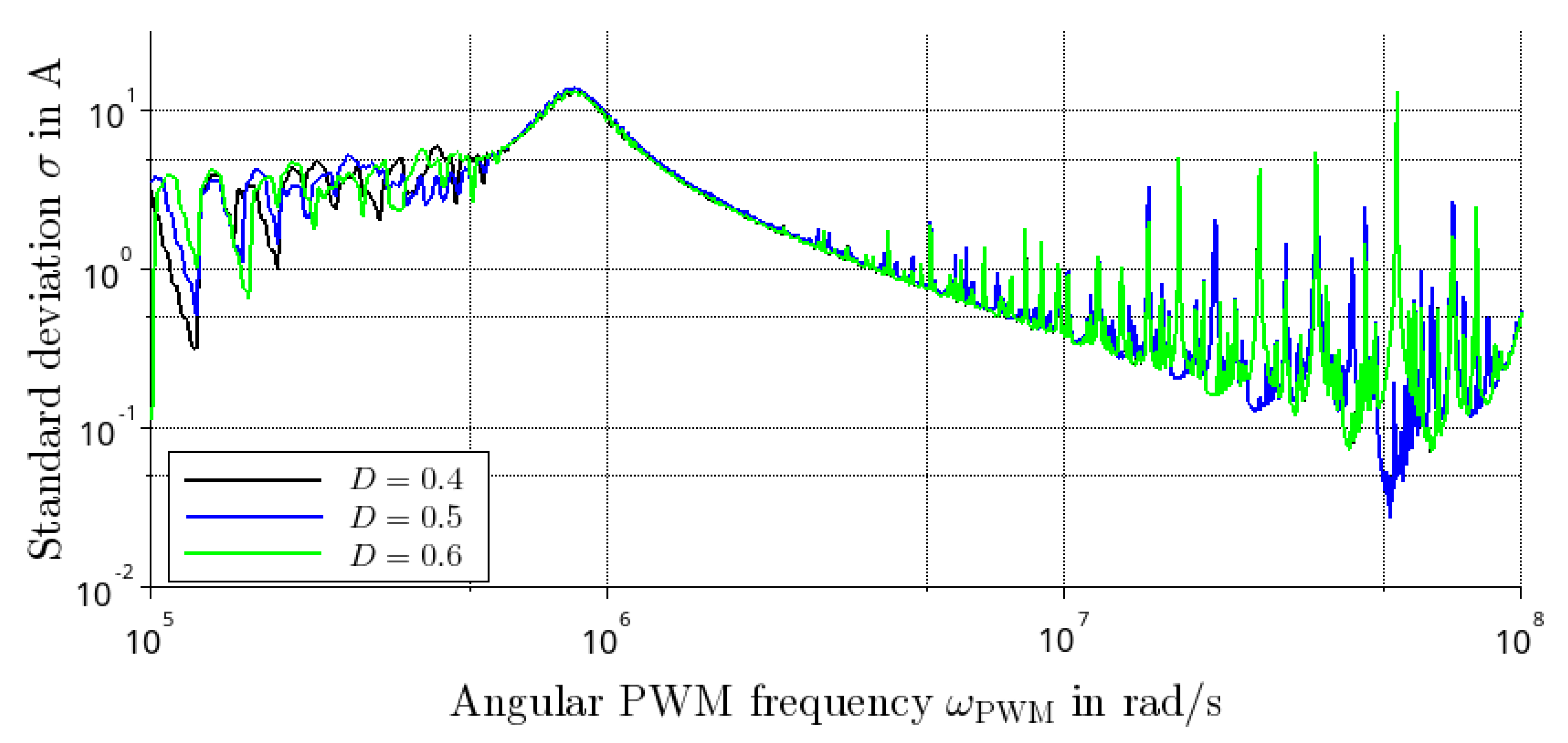
The frequency response is the gain factor of the system’s steady-state response to harmonic (i.e., sinusoidal) excitations for different angular frequencies. However, in the case of switched converters, the excitation is not sinusoidal, but by means of PWM signals. The PWM signals are periodic and can be expanded into a Fourier series. The switching frequency is the fundamental frequency, but there are also higher harmonics that also depend on the duty cycle. The higher harmonics can possibly excite resonance frequencies in the higher frequency spectrum. To investigate this problem we excited the discretized model of the distributed converter with different PWM signals. The transient simulations were carried out over a duration of  100 μ s . The ripples occur in the current transients as shown in Figure 5. To measure these ripples in a near steady-state situation we computed the standard deviation  σ of the current transients in the last 10 of the simulation time, i.e., for the range between t = 90 μ s and t = 100 μ s . To compare the results with the amplitude frequency response shown in Figure 7, the current standard deviation in dependence on the angular PWM frequency ω PWM = 2 π f PWM is shown in Figure 8 using a logarithmic plot. We used a slightly smaller frequency range as in Figure 7, but included the first angular resonance frequency  ω 0 and the angular antiresonance frequency  ω 1 .
The curves shown in Figure 8 are roughly similar to the frequency response shown in Figure 7, especially near the first resonance frequency  ω 0 . We plotted the standard deviation computed for different duty ratios D { 0.4 , 0.5 , 0.6 } , whereby there is a considerable qualitative similarity between the curves. Below the resonance frequency  ω 0 , the low-pass filter, which results from the line inductance, the external capacitor and the load resistance, has hardly any effect. As a result, relatively large fluctuations occur in the standard deviation. From the resonance frequency ω PWM = ω 0 up to about ω PWM 3 × 10 6 rad / s , a continuous drop in the standard deviation can be seen, which is due to the low-pass behavior. At higher frequencies, peaks occur more and more strongly, which can be explained by the forward and backward traveling waves in the transmission line in the time domain or by resonance peaks excited by higher harmonics in the frequency domain. We see a significant drop in the standard deviation near the antiresonance frequency  ω 1 for D = 0.5 . On the other hand, we have resonances for D = 0.4 and D = 0.6 in this frequency range. This can be explained as follows: Resonances and antiresonances alternate for multiples of the first antiresonance frequency. For D = 0.5 , the Fourier series of the PWM signal (with the exception of the constant term) only contains odd coefficients. This means that only antiresonances are excited, so that current ripples are mostly suppressed. For D 0.5 , the Fourier series of the PWM signal also contains even harmonics, which excite resonances and thus lead to current ripples.
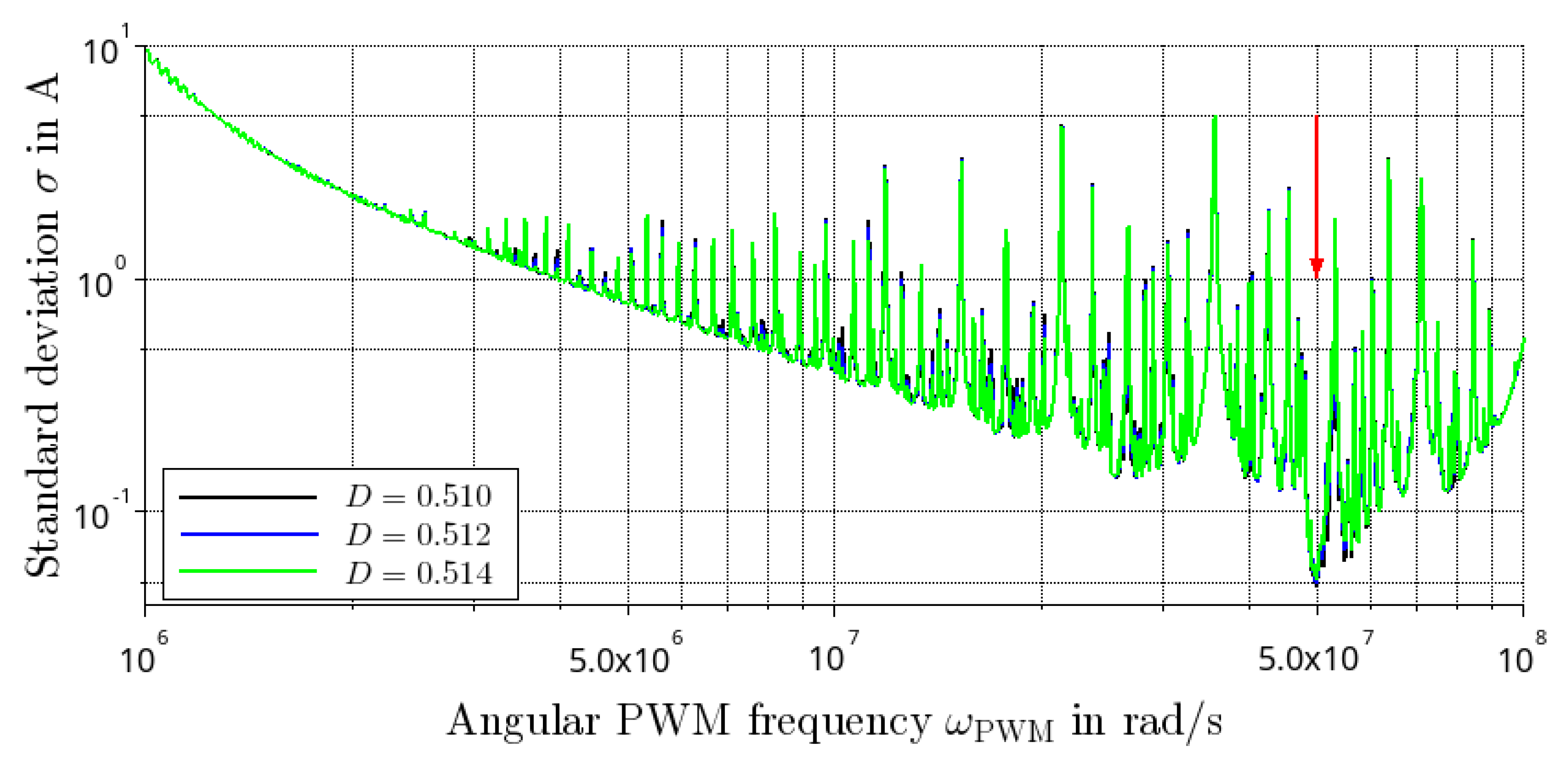
Figure 8 shows that the antiresonance frequency was different at different duty cycles. A more in-depth analysis is therefore necessary for the desired operating point. In Section 3.4, for the desired output voltage v 0 = 6 V , the input signal d 0 0.512 was determined based on an averaged model. For the switched model, the duty cycles D { 0.510 , 0.512 , 0.514 } that lie in the neighborhood of this operating point should therefore be considered. Figure 9 shows the standard deviation as a function of the angular PWM switching frequency for the range restricted to the higher frequencies. It can be seen that a significant reduction in the standard deviation is achieved in the region of ω PWM 5 × 10 7 rad / s for all duty cycles considered. Here there is obviously a noticeable antiresonance frequency. This frequency is marked with a red arrow in the diagram.

5. Closed Loop Control

5.1. Control Structure and Static Prefilter

The desired control variable is the output voltage v ( l , t ) on the right hand side of the transmission line. For a useful implementation, the control and measurement should take place at the same side of the transmission line. A voltage is fed into the left hand side of the transmission line via the PWM-controlled switch. It therefore makes sense to measure the current i ( 0 , t ) on the left-hand side and use it for control. In addition, the duty ratio is limited to D [ 0 , 1 ] . This restriction is ensured by a saturation block. The resulting structure of the closed control loop is shown in Figure 10. The resulting input-output behavior of the plant has already been taken into account in the transfer function (20).
The fact that we want to specify a reference voltage, but only have the current available for the control, makes a conversion from voltage to current necessary. This conversion is performed via the static prefilter. From the equilibrium condition (26) of the finite dimensional model of the classical converter we obtain the scaling factor
F = G C R + 1 R 1 R = 0.1 S .
Interestingly, this conversion does not include the conduction losses  R L of the inductor, but only the insulation losses  G C of the capacitor (and of course the resistance R of the load). However, the insulation losses are extremely low, so that only the load is relevant.

5.2. Controller Design

For angular frequencies up to ω 10 7 rad / s , the frequency responses of the classic converter with discrete components and the converter with the transmission line agree very well as shown in Section 4.2. The transfer function (4) respectively (32) of the classic converter should therefore be used for a controller design in the frequency range, but then used for the distributed converter.
DC/DC converters are very often regulated with proportional-integral controllers (PI controllers), see e.g. [1,15,16]. In the frequency domain, PI controllers can be described by the transfer function
G ( s ) = k 1 + 1 s T i
= k p + k i s .
Equation (38) is the standard form of the PI controller with the gain k and the integral time constant  T i . This form is helpful for the controller design, whereas the parallel form (39) with the proportional gain k p = k and the integral gain k i = k / T i is often is used for implementation.
There are many different methods and approaches for designing PI controllers [26,27]. Since the plant’s transfer function (32) is comparatively simple as a second-order system, we will carry out the controller design directly in the frequency domain. For this reason we consider the open loop transfer function having the form
P ( s ) · G ( s ) = k b 1 s + b 0 s 2 + a 1 s + a 0 · 1 + s T i s T i ,
where the coefficients a 0 , a 1 , b 0 , b 1 result from the transfer function (32) of the plant. The transfer function (40) is unstable due to the integral part of the controller, which can be recognized by the pole at the origin. First of all, the closed loop system should be stable. In addition, the oscillations that occur in the plant should be suppressed in the closed control loop.
Due to the low inductance of the transmission line, the radian resonant frequency  ω 0 of the equivalent conventional converter is comparatively high. In practice, the required settling times typically correspond to significantly lower frequencies. The integral time constant is selected with T i = 10 μ s such that the folding frequency ω i = 1 / T i = 10 5 rad / s is approximately one order of magnitude below the resonance frequency. Figure 11 shows the amplitude frequency responses of the plant’s transfer function (32) as well as the open loop transfer function (40) with k = 1 . A discussion on the choice of the controller time constants can be found in ([1], Section 8.2.2).
The gain k must still be determined for the PI controller. We will use the root locus technique, which provides a design method based on the system’s open loop transfer function [28]. With this method, the poles of the closed loop system are plotted in the complex plane as a function of the gain k.
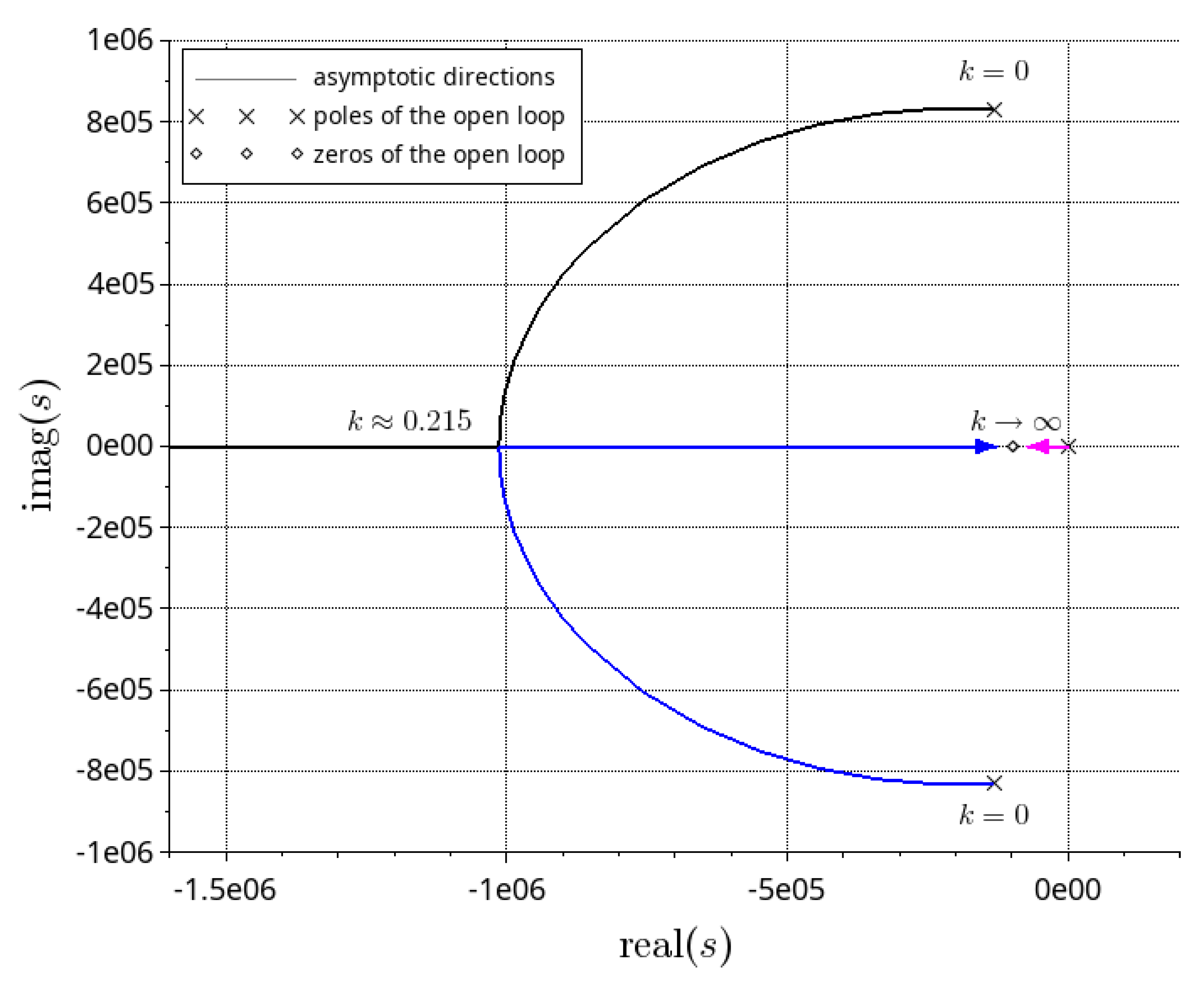
The root locus plot of the open loop transfer function (40) is shown in Figure 12. The root loci start for k = 0 at the poles of the open loop transfer function, i.e, at a conjugate complex pair located in the left half plane resulting from the plant (32) and a pole in the origin resulting from the integral part of the PI controller. From k 0.214 , the conjugate complex pole pair merges into two real poles on the real left half axis. A double real pole occurs at this transition, whereby the associated gain can be calculated in Scilab using the function krac2. For k , the root loci converge to the zeros of the open loop transfer function. We have one real zero at s 99940 due to the plant’s transfer function (32) and another real zero at s = 1 / T i = 100000 from the PI controller. These zeros are located on the real left half axis and cannot be distinguished visually in Figure 12. Two branches of the root locus plot converge to these zeros. Since the open loop transfer function has one zero less than poles, the third branch on the root locus plot converges to s .
From the root locus plot we draw the following conclusions: For any k > 0 the closed loop system is stable. With k 0.214 the system has solely real poles, i.e., so that no oscillations occur. In our simulation we will use gain k = 5 . In general, the controller gain should not be set too high for buck converters, because the input saturation of the duty cycle may lead to a controller windup [29].

5.3. Closed Loop Transient Simulation

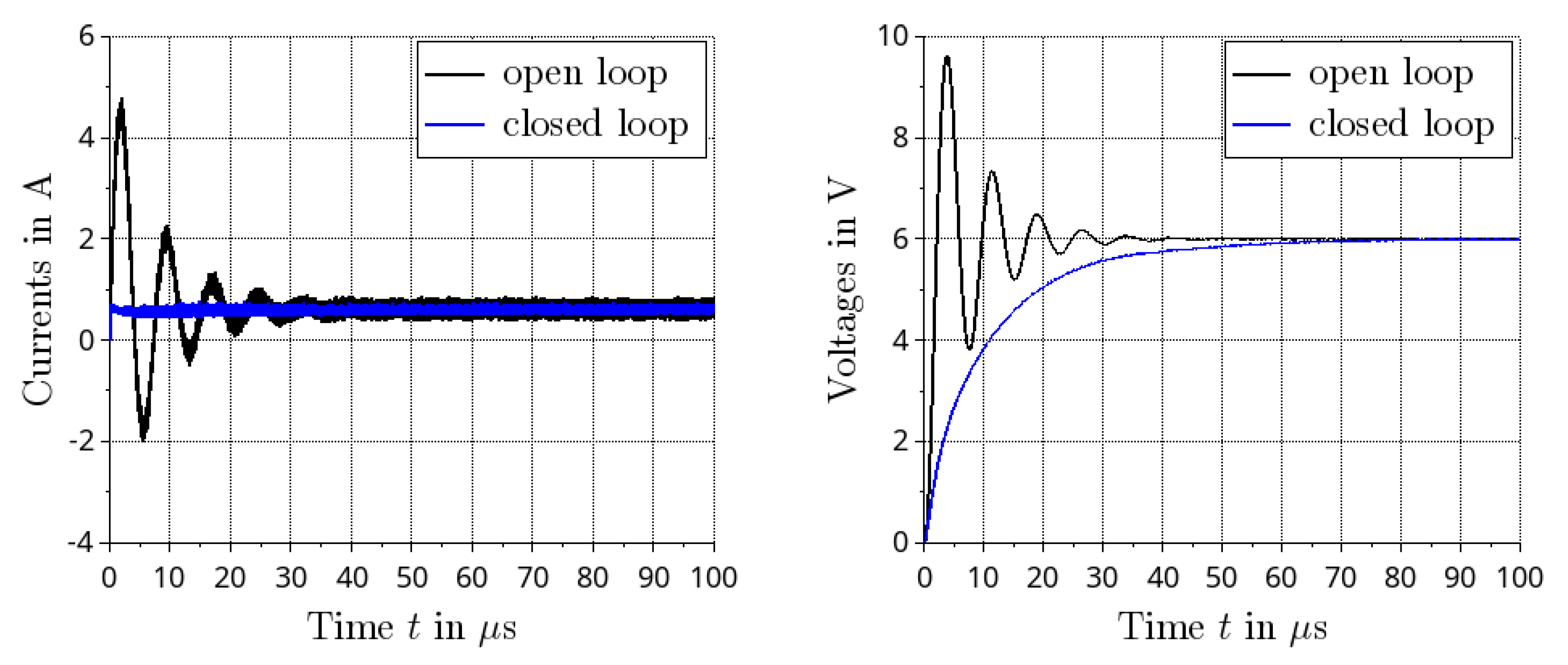
The simulation is to be carried out on the discretized distributed converter model. The PWM frequency must still be defined for the simulation. The PWM frequency should be chosen such that current ripples are largely suppressed. In Section 4.3 we observed an antiresonance area around ω PWM 5 × 10 7 rad / s . This leads to the technical PWM frequency f PWM 7.957747 M H z . As with the simulations before, we want to obtain the output voltage of 6 V . The transient simulation results of the open and closed control loop of the discretized distributed buck converter are shown in Figure 13. The controller suppresses the oscillations that occur in the open control loop. The desired output voltage is achieved. There are only comparatively small ripples in the current. The controller designed for the classic converter also works with the distributed converter.

6. Discussion

In the paper, a buck converter was analyzed in which the inductor was replaced by a transmission line. Converter topologies with a transmission line are comparatively rarely discussed in the literature. In contrast to [2,3], the distributed converter model discussed in the article is not just an intermediate step for a different setup with several discrete components, but could be used in such a way that the power inductor can actually be saved. When compared to the models considered in the previous papers [5,6,7], the model in this contribution also contains an external capacitor.
Converters with a transmission line are distributed parameter systems described by PDEs. In general, there are two basic strategies for designing controllers for distributed systems. In the case of early lumping, the distributed system model is discretized and then the controller is designed. Classic design methods can be used for this purpose. In the case of late lumping, the controller is designed for the distributed model. This approach usually leads to a distributed controller model, which is then discretized for the implementation. This design approach is generally more difficult. The controller in [30] was derived in the time domain on the basis of a control Lyapunov functional and was then approximated for the implementation. The result is a nonlinear switching controller that excites the converter circuit in a very high frequency range. In this article, the controller design was based on an approximation of the plant’s model in the frequency domain resulting in a linear controller.
With a PI controller, a linear and comparatively easy to implement analog controller was used. In principle, implementation with a digital controller would also be possible. With this, however, the current measurement should be synchronized with the pulse width modulation. More complex controller strategies could then be used, e.g. internal model control [31,32,33].
The investigations in Section 4 show that the classical and the distributed converter have a similar amplitude response over a wide frequency range. The behavior of the distributed converter can be divided into two frequency ranges. On the one hand, the external capacitor leads to a significantly lower first resonance frequency compared to [6,7]. In this frequency range, the behavior of the distributed converter resulting from a transcendental transfer function can be adequately described by a Padé approximant having the same order as the rational transfer function of the classical converter. This frequency range is used for the approximation and the subsequent controller design. The alternating resonance and antiresonance frequencies in the higher frequency range are caused by the transmission line. However, these frequencies can also be lowered by using a longer transmission line.
The coaxial cable used here is primarily intended for signal transmission and not for transmitting power. The coaxial cable was used because the parameters of this cable are very well known and it is also supported by circuit simulators. A twisted-pair cable would certainly make more sense for practical and economical implementation. Microstrips would also be conceivable for smaller implementations on a printed circuit board [34].
Of course, the question arises as to whether this approach could also be relevant for other types of switched-mode converters. If a supply line is to be used meaningfully as an inductor, in the conventional converter circuit the inductor must be in series between the power supply and the load. This for example does not apply to the buck-boost converter, see [2] and [3]. In addition, the manipulated variable and the feedback variable should be on the same side of the transmission line, as otherwise another signal line would be necessary. In this article, the left-hand side (supply side) was considered, whereby the voltage was fed in and the current was measured for the control. The right-hand side (load side) would be suitable for the boost converter [4]. The incorporation of transmission lines into the models can certainly also be of interest for applications in electric drives and the power grids where AC and multilevel converters are used [8,35,36,37], which would be subject of further research.

Author Contributions

Conceptualization, K.R. and D.G; methodology, D.G.; software, K.R.; validation, D.G.; formal analysis, K.R. and D.G.; writing—original draft preparation, K.R.; writing—review and editing, D.G.; visualization, K.R.; supervision, K.R.; All authors have read and agreed to the published version of the manuscript.

Funding

This research received no external funding.

Institutional Review Board Statement

Not applicable.

Informed Consent Statement

Not applicable.

Data Availability Statement

No measured data was used for this article. The software (Scilab scripts) will be made available by the authors on request.

Conflicts of Interest

The authors declare no conflicts of interest.

Abbreviations

The following abbreviations are used in this manuscript:
AC alternating current
DC direct current
ODE ordinary differential equation
PDE partial differential equation

References

  1. Bacha, S.; Munteanu, I.; Bratcu, A.I. Power Electronic Converters Modeling and Control; Springer-Verlag: London, 2014. [Google Scholar]
  2. Sander, S. Buck and boost converters with transmission lines. IEEE Transactions on Power Electronics 2012, 27, 4013–4020. [Google Scholar] [CrossRef]
  3. Sander, S.; Karvonen, A. Semiconductor component reduction in AC/DC converters with transmission lines. In Proceedings of the 15th European Conference on Power Electronics and Applications (EPE), 2013, p. 1–10.
  4. Röbenack, K.; Bärnklau, H. A Spatially Distributed Boost Converter – Modeling and Simulation. In Proceedings of the International Conference on System Theory, Control and Computing (ICSTCC), Timisoara, Romania; 2023; pp. 480–486. [Google Scholar] [CrossRef]
  5. Huang, C.; Woittennek, F.; Röbenack, K. Steady-state analysis of a distributed model of the buck converter. In Proceedings of the European Conference on Circuit Theory and Design (ECCTD); 2013; pp. 1–4. [Google Scholar] [CrossRef]
  6. Röbenack, K.; Herrmann, R. Analysis, Simulation and Implementation of a Distributed Buck Converter. In Proceedings of the 26th International Conference on System Theory, Control and Computing (ICSTCC), Sinaia, Romania; 2022; pp. 213–218. [Google Scholar] [CrossRef]
  7. Röbenack, K.; Herrmann, R. Distributed Buck Converter Realization Based on a Transmission Line. SYSTEM THEORY, CONTROL AND COMPUTING JOURNAL 2023, 3, 29–35. [Google Scholar] [CrossRef]
  8. Zainea, M.; van der Schaft, A.; Buisson, J. Stabilizing control for power converters connected to transmission lines. In Proceedings of the Proc. American Control Conference (ACC); 2007; pp. 3476–3481. [Google Scholar] [CrossRef]
  9. Daafouz, J.; Tucsnak, M.; Valein, J. Nonlinear control of a coupled PDE/ODE system modeling a switched power converter with a transmission line. Systems & Control Letters 2014, 70, 92–99. [Google Scholar] [CrossRef]
  10. King, W.P. Transmission Line Theory; Dover Publications, Inc., 1965.
  11. Mathis, W.; Reibiger, A. Küpfmüller Theoretische Elektrotechnik, 20th ed.; Springer Vieweg, 2017. [CrossRef]
  12. Sira-Ramírez, H. Nonlinear P-I Controller Design for Switchmode dc-to-dc power converters. IEEE Trans. on Circuits and Systems 1991, 38, 410–417. [Google Scholar] [CrossRef]
  13. Escobar, G.; Ortega, R.; Sira-Ramirez, H.; Vilan, J.P.; Zein, I. An experimental comparison of several non linear controllers for power converters. IEEE Control Systems 1999, 19, 66–82. [Google Scholar]
  14. Kugi, A.; Schlacher, K. Nonlinear H-Controller Design for a DC-to-DC Power Converter. IEEE Trans. on Control Systems Technology 1999, 7, 230–237. [Google Scholar] [CrossRef]
  15. Duong, M.Q.; Sava, G.N.; Scripcariu, M.; Mussetta, M.; et al. Design and simulation of PI-type control for the Buck Boost converter. In Proceedings of the 2017 International Conference on Energy and Environment (CIEM). IEEE; 2017; pp. 79–82. [Google Scholar] [CrossRef]
  16. Garg, M.M.; Hote, Y.V.; Pathak, M.K.; Behera, L. An approach for buck converter PI controller design using stability boundary locus. In Proceedings of the 2018 IEEE/PES Transmission and Distribution Conference and Exposition (T&D). IEEE, 2018, p. 1–5. [CrossRef]
  17. Tzafestas, S.G. Distributed parameter control systems: Theory and application; Vol. 6, International Series on Systems and Control, Pergamon Press: Oxford, UK, 2013.
  18. Christofides, P.D.; Daoutidis, P. Feedback control of hyperbolic PDE systems. AIChE Journal 1996, 42, 3063–3086. [Google Scholar] [CrossRef]
  19. Deutscher, J.; Harkort, C. A parametric approach to finite-dimensional control of linear distributed-parameter systems. International Journal of Control 2010, 83, 1674–1685. [Google Scholar] [CrossRef]
  20. Dimirovski, G.; Gough, N.; Barnettj, S. Categories in systems and control theory. International Journal of Systems Science 1977, 8, 1081–1090. [Google Scholar] [CrossRef]
  21. TimKabel. RG 58 C/U 50 Ω, Coaxial cable. http://www.tim-kabel.hr/images/stories/katalog/datasheetHRV/1502_RG58_ENG.pdf.
  22. LAPP. RG-58 C/U, 2020. https://e.lapp.com/apac/p/coaxial-cables/coaxial-rg-58-c-u-217000.
  23. Scilab. http://www.scilab.org/.
  24. Maxima, a Computer Algebra System. http://maxima.sourceforge.net.
  25. The Sage Developers. SageMath, the Sage Mathematics Software System (Version 10.2), 2024. https://www.sagemath.org.
  26. Marlin, T.E. Process Control, Designing Processes and Control Systems for Dynamics Performance, 2 ed.; McGraw-Hill, 2000.
  27. O’Dwyer, A. Handbook of PI and PID controller tuning rules; Imperial College Press: London, 2009. [Google Scholar]
  28. Dutoon, K.; Thompson, S.; Barraclough, B. The Art of Control Engineering; Prentice Hall, 1997.
  29. Hippe, P. Windup in Control: Its Effects and Their Prevention; Springer-Verlag: London, 2006. [Google Scholar]
  30. Röbenack, K.; Palis, S. Set-Point Control of a Spatially Distributed Buck Converter. Algorithms 2023, 16. [Google Scholar] [CrossRef]
  31. Economou, C.G.; Morari, M. Internal Model Contrl. 5. Extension to Nonlinear Systems. Ind. Eng. Chem. Process Des. Dev. 1986, 25, 403–411. [Google Scholar] [CrossRef]
  32. Henson, M.A.; Seborg, D.E. An internal model control strategy for nonlinear systems. AIChE Journal 1991, 37, 1065–1081. [Google Scholar] [CrossRef]
  33. Datta, A. , 1998; p. 47–58.Schemes. In Adaptive Internal Model Control; Springer: London, 1998; pp. 47–58. [Google Scholar]
  34. Lacoste, R. Robert Lacoste’s The Darker Side: Practical Applications for Electronic Design Concepts from Circuit Cellar; Newnes, 2009.
  35. Lupo, G.; Petrarca, C.; Vitelli, M.; Tucci, V. Multiconductor transmission line analysis of steep-front surges in machine windings. IEEE Transactions on Dielectrics and Electrical Insulation 2002, 9, 467–478. [Google Scholar] [CrossRef]
  36. Bärnklau, H.; Gensior, A.; Rudolph, J. A model-based control scheme for modular multilevel converters. IEEE Transactions on Industrial Electronics 2012, 60, 5359–5375. [Google Scholar] [CrossRef]
  37. Xie, Y.; Zhang, J.; Leonardi, F.; Munoz, A.R.; Degner, M.W.; Liang, F. Modeling and verification of electrical stress in inverter-driven electric machine windings. IEEE Transactions on Industry Applications 2019, 55, 5818–5829. [Google Scholar] [CrossRef]
Figure 1. Standard buck converter, circuit diagram (left), network model considering losses (right).
Preprints 111065 g001
Figure 2. Distributed buck converter with transmission line.
Preprints 111065 g002
Figure 3. Distributed buck converter with discretized transmission line.
Preprints 111065 g003
Figure 4. Step response of the state-space models of the standard and the discretized distributed buck converter.
Preprints 111065 g004
Figure 5. Analog PWM generation, PWM and reference sawtooth signals (left), sketch of an implementation with an operational amplifier used as a comparator circuit (right).
Preprints 111065 g005
Figure 6. Responses of the state-space models of the standard and the discretized distributed buck converter under PWM excitation with different frequencies.
Preprints 111065 g006
Figure 7. Amplitude frequency responses of the transfer functions.
Preprints 111065 g007
Figure 8. Standard deviation of the current peaks in the range between t = 90 μ s and t = 100 μ s of the simulated distributed converter under PWM excitation for duty ratios D { 0.4 , 0.5 , 0.6 } .
Preprints 111065 g008
Figure 9. Standard deviation of the current peaks in the range between t = 90 μ s and t = 100 μ s of the simulated distributed converter under PWM excitation for duty ratios D { 0.510 , 0.512 , 0.514 } .
Preprints 111065 g009
Figure 10. Closed loop control structure.
Preprints 111065 g010
Figure 11. Amplitude frequency responses of the plant’s transfer function (32) as well as the open loop transfer function (40) including the PI controller with k = 1 .
Preprints 111065 g011
Figure 12. Root locus plot of (40) for k 0 .
Preprints 111065 g012
Figure 13. Transient simulation of the state-space model of the discretized distributed buck converter in open and closed control loop.
Preprints 111065 g013
Disclaimer/Publisher’s Note: The statements, opinions and data contained in all publications are solely those of the individual author(s) and contributor(s) and not of MDPI and/or the editor(s). MDPI and/or the editor(s) disclaim responsibility for any injury to people or property resulting from any ideas, methods, instructions or products referred to in the content.
Copyright: This open access article is published under a Creative Commons CC BY 4.0 license, which permit the free download, distribution, and reuse, provided that the author and preprint are cited in any reuse.
Alerts
Prerpints.org logo

Preprints.org is a free preprint server supported by MDPI in Basel, Switzerland.

Subscribe

© 2025 MDPI (Basel, Switzerland) unless otherwise stated