1. Introduction
Island-bridge structures are a popular concept towards building flexible electronics, where the islands as the rigid part are incorporated into a soft and stretchable material and connected by metal bridges to create the electrical functionality. Although it cannot compete with flexible material-based structures, where every component is stretchable, the island-bridge concept has the advantage, that conventional high-performance devices can be placed on these islands, where they are isolated from strain [
1,
2].
There are different ways to build the flexible interconnects between the islands. One possibility is to fabricate the devices and metal lines in a standard process and transfer them onto a pre-stretched substrate. Releasing the pre-stretch pops up the bridges from surface, so that they have an arc-shaped structure and can tolerate a specific amount of strain [
3,
4,
5]. By using trenches, which separate the islands from each other, the pre-stretch can also be used to let the metal lines buckle into the depth of the trench [6]. Of course, this transfer process is difficult to implement in a conventional processing route. Hence, there is also the possibility to use the silicon substrate itself and structure it from the front- and backside into islands [7]. The benefit of this approach is that the whole process stays within the standard planar technology, which simplifies handling and production. But on the other side building 3D arc-shaped bridges using the trench depth is not an option anymore. Consequently, complex designs like mesh structures or combination of specific beam structures must be used, for the flexible interconnects, [
7,
8,
9].
In this paper we show detailed investigations for our alternative manufacturing route which we use for fabricating stretch-free shape induced interconnects [10]. Here, the focus is on the trench depth as a key parameter. Numerical simulations were used to figure out the influence of the trench depth on the stress distribution of the metal bridge. An analytical model for explaining the stress behavior is established. Additionally, process optimization parameters for the fabrication of such advanced metal bridge structures are shown.
2. Materials and Methods
2.1. Integration Concept
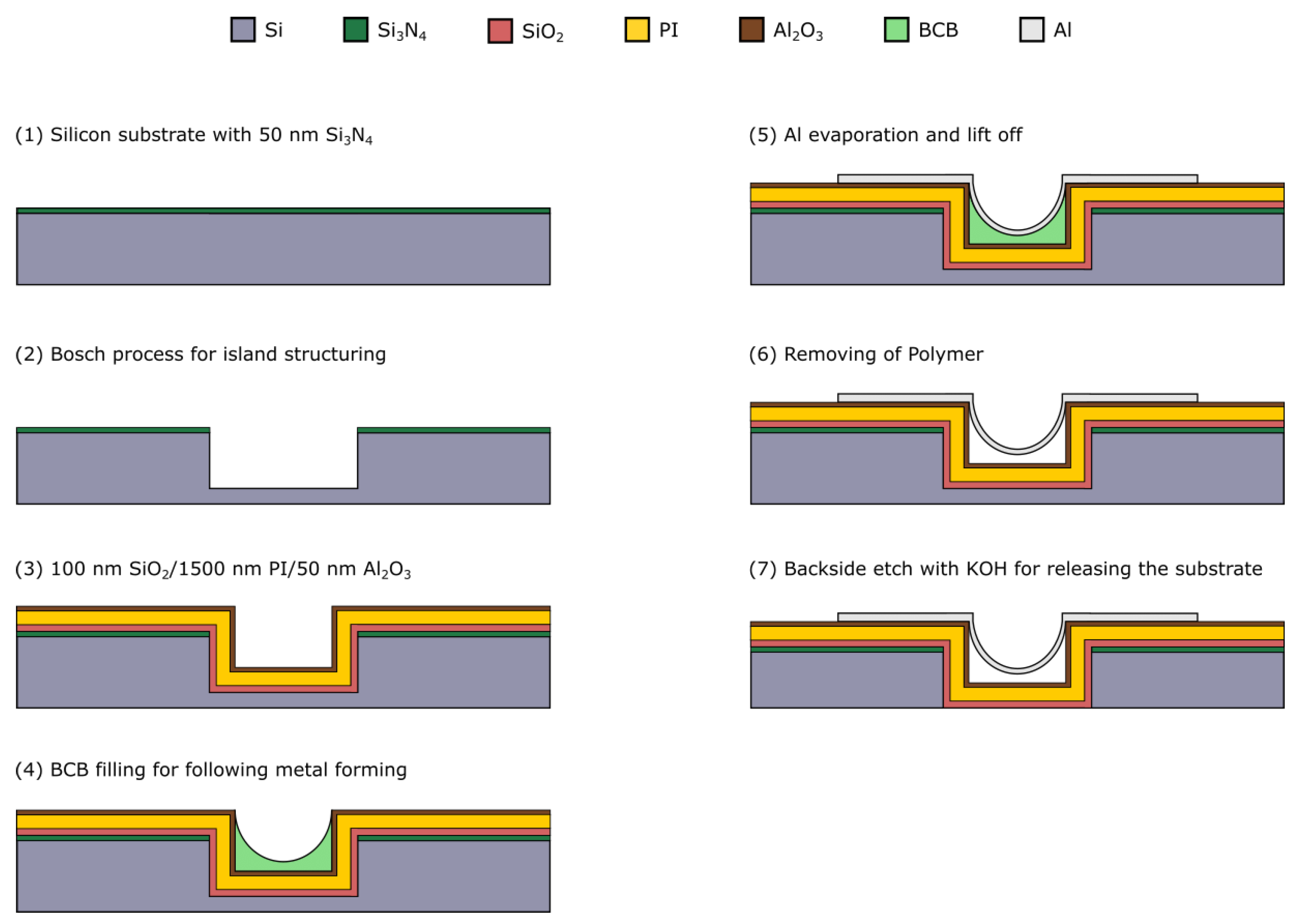
In our previous paper we introduced the alternative concept to fabricate arc-shaped freestanding metal bridges into the trench depth (
Figure 1). The in this way created 3D structures work as flexible interconnects between silicon islands and are completely integrated into the silicon planar technology. The concept also includes a flexible substrate (
Figure 1, Polyimide) that simultaneously functions as a passivation layer [10].
Before structuring the trenches, it is also possible to fabricate electronic devices on the subsequently formed islands. After the Polyimide (PI) is spin coated the metal lines are structured into the trench depth by using a forming process with a polymer, which is also spin coated. Finally, step 7 is used to remove the backside of the silicon wafer and to release the island-bridge substrate. With this last step the substrates also get semi-transparent.
The structures were investigated by using 2D simulations regarding to geometry parameters. While it turned out that the stress distribution is similar to a bending under uniform line load it also shows that the trench depth can have the most positive effect to the stress distribution compared to metal width, thickness and trench width. With the detailed investigations here, we want to give an explanation about this impact of the trench depth.
The forming process for the metal bridges was done by using Benzocyclobutene (BCB), which was spin coated into the trenches. The subsequently cleaning of the trenches to get freestanding metal lines worked out, but also can cause damage to the interconnects as the functionality test showed. All structures had a deviation in the resistance compared to a theoretical calculated value. Some interconnects did not work at all, which was a problem of defects. These results showed that an optimization of the process is needed. So, the focus of this work was set to step 4 to 6 of the manufacturing route (
Figure 1).
2.2. Design of Numerical Modelling
The numerical simulations are performed using Ansys Mechanical 2022 R1 and with the same material parameter as in our first study [10].
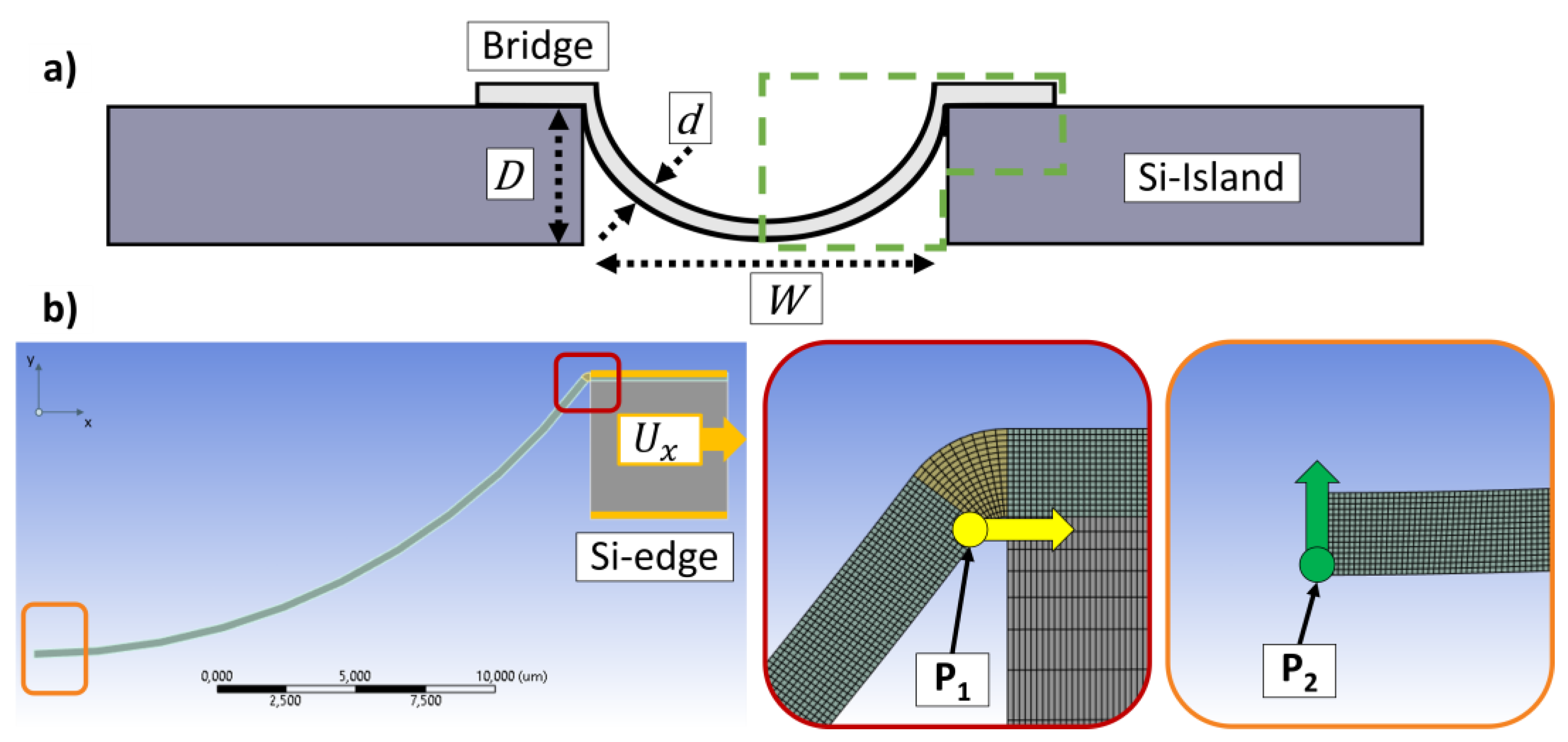
Figure 2 a) shows a schematic drawing of the geometry illustrating the trench depth
D, trench width
W and the metal thickness
d. While
W and
d were set constant at 40 µm and 300 nm respectively, the trench depth
D was varied to 5, 10, 15 and 20 µm. The simulations discussed here are focused on the trench depth optimization, as it is anticipated to be the key factor for increasing the strain, which the metal can hold in the region of elastic deformation [10]. The upper limit of the elastic deformation is called the yield strength
γs and serves here as the maximum acceptable value for the stress in the bridge. The green box in
Figure 2 a) displays the part of the concept, which was modeled in a symmetrical 2D simulation as can be seen in
Figure 2 b).
Since silicon is a rigid material, not the entire island is built in the model but only the upper corner where the metal bridge arrives. As a load a displacement
Ux is applied at this silicon edge to have a stretching of the structure in
x direction. First the
Ux was set to 0.34 µm, which was sufficient to reach the yield strength
γs of the metal bridge over the 5 µm deep trench. In a second approach, depending on the trench depth
D, a specific displacement to the silicon edge was applied to reach
γs of the corresponding structure. The values for
Ux for the before mentioned trench depth variations were 0.34, 1.13, 2.57 and 3.98 µm. For both simulations the movement in
x direction of point
P1 at the upper end of the metal was compared to the movement in
y direction for point
P2 in the middle (cf.
Figure 2).
2.3. Material Processing
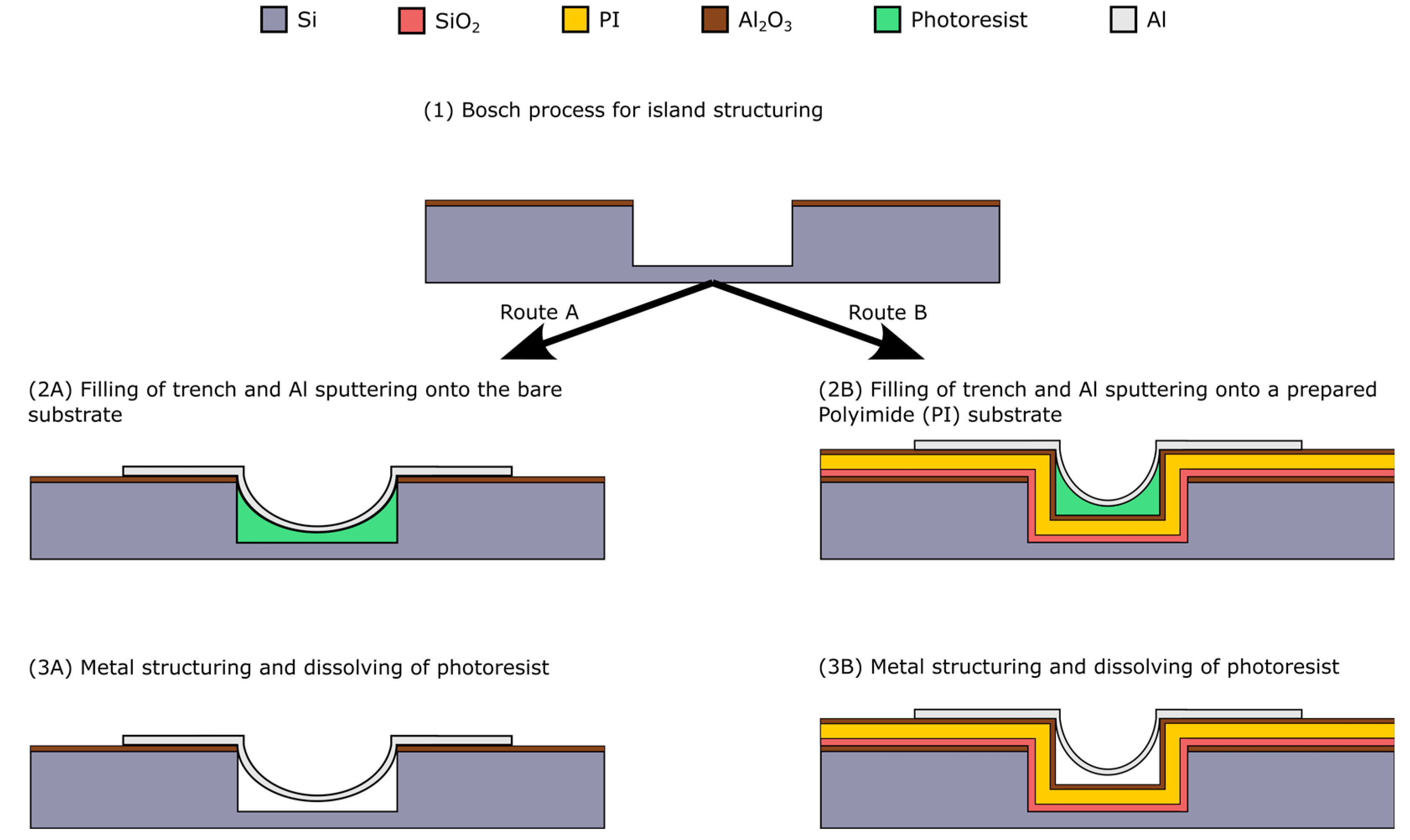
Here, as mentioned in section 2.1, we focused our work on optimizing the metal deposition and the patterning. That means we reduced the complete process flow of
Figure 1 to the fabrication scheme in
Figure 3. So, we skipped the final step which would be a wet chemical etching with potassium hydroxide (KOH) on the backside of the wafer and which is used to release the complete island-bridge substrate to make it flexible Typically, array structures were fabricated, where th width of the trenches is kept constant at 40 µm, while the bridges are varying between 5, 10, 20 and 30 µm in width..
Figure 3 depicts the corresponding steps, wherein route A is focusing on the formation of the arc shape structure. For the filling of the trenches a photoresist AZ5214 from MicroChemicals is used. To investigate the filling behavior, the resist was spin coated with 1000, 2000 and 3000 rpm and trench depths of 10 and 20 µm are used. Finally, the process is transferred to the reference process surface, which includes a PI layer to provide a flexible matrix for the islands (
Figure 3, route B). The PI is spin coated with 3000 rpm and then cured during a temperature ramp up of 300 °C, at which it holds for 1 hour. Subsequent to the trench filling 500 nm aluminum (Al) is deposited by sputtering and structured either by wet chemical or by dry etching. For the wet chemical etching TechniEtch Al80 from MicroChemicals is used. The dry etching is performed in a Plasmalab System100 from Oxford Instruments with a mixture of chlorine (Cl) and hydrogen bromide (HBr). Thereafter, the resist is ashed in a TEPLA Plasma chamber with an O
2-Plasma at 300 W for 10 min, to yield/release freestanding metal bridges.
2.4. Electrical Characterisation
The conductivity of the previously mentioned structures is verified by current-voltage measurements on interconnect loops over 96 islands in an array configuration. The structures were designed such that one loop runs back and forth so that contact 1 and contact 2 are next to each other. The measurements are performed by applying a current sweep from -90 µA to +90 µA with steps of 20 µA and measuring the required voltage between contact. The functionality of the structures is evaluated based on the determined resistance R, which is compared to theoretical resistance Rtheo of the bridges. The theoretical value is calculated by using the specific resistance of Al from the literature [11]. For the geometrical dimension of the structures the length was taken from the mask layout and for thickness 500 nm was used. These current voltage measurements are an easy way to determine the yield of the bridges regarding to trench and metal width.
3. Results
3.1. Numerical Simulations
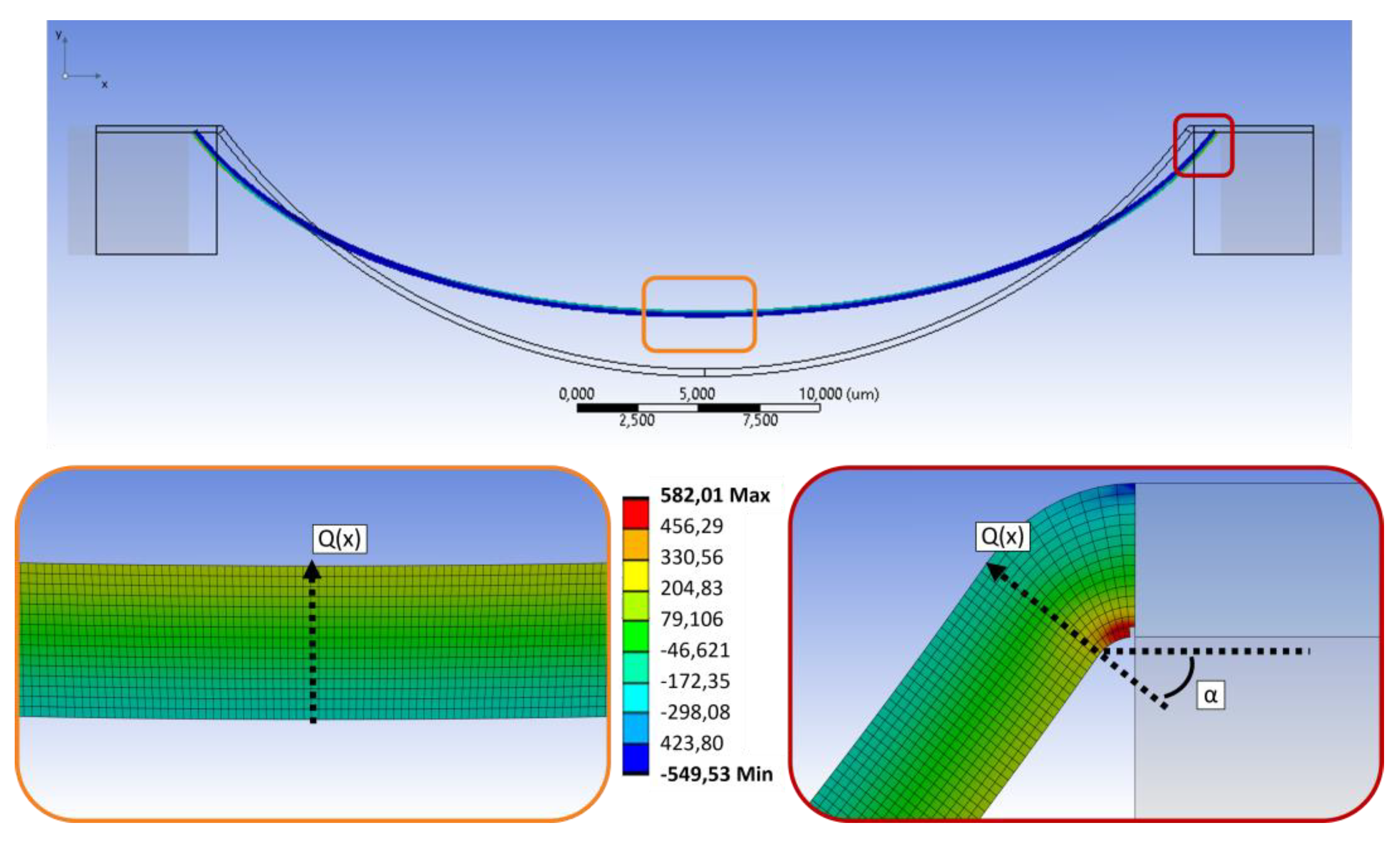
Figure 4 shows the behavior of the bridge going through a 10 µm deep trench under tensile load. The top image depicts a comparison of the deformed and undeformed model. As can be seen, the deformation in
x direction causes a movement upwards of the middle section. In the detailed views the stress distribution along the metal is displayed. For the middle part (orange frame) the stress is positive (tensile) at the upper edge and negative (compressive) at the bottom. Contrary to this at the support of the bridge (red) the tensile stress occurs at the bottom side and the compressive stress on the opposite. Such a stress distribution is also known from the pure bending of a straight beam under line load, which can be described as uniaxial stress state, where the stress
σx at every position can be calculated with the following equation [12]:
Here,
M is the bending moment,
Iy the geometrical moment of inertia and
z the distance to the neutral plane [12]. The yield strength
γs as the maximum tolerated value can be applied for
σx and the corresponding bending moment can be calculated. In our model
γs was set to 545 MPa which is a reported value for the targeted very thin metal lines (200-300 nm) [13]. Using equation 2 and 3 together with the length
l of the beam, the line load
q(x) and the shear force
Q(x) can be obtained:
For the derivation of these equations a differential equation of 4th order with specific boundary conditions is used to calculate a special bending case [12]. As can be seen in Figure 4,
γs is most likely be reached on the upper end of the bridge at the transition to the island. Also, the direction of the shear force
Q(x) and the angular between the horizontal plane and this directed force is marked. That means at this point, knowing these two components, that the force in
x direction, which is caused by the applied movement, can be calculated via a trigonometric function. The details are given in
Appendix A. Finally, the resulting deformation in
x direction can be determined and used for the simulation to compare the movement of
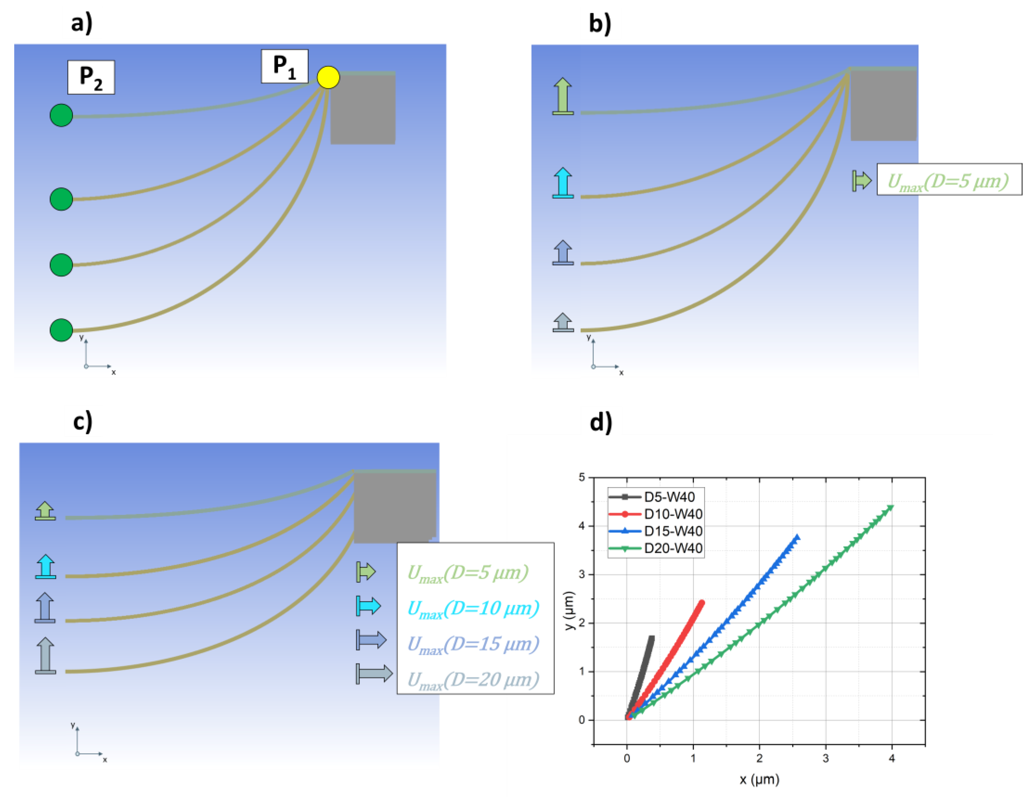
P1 and
P2. The results are illustrated in
Figure 5. For a better comparability in
Figure 5 a) - c) the individual snapshots of each geometry variation were placed in one picture.
As described in section 2.1 the simulation was done with bridges, which go through different trench depths
D. So, the interconnect in the 5 µm deep trench (D5-W40) is the flattest and therefore always the upper one, while the metal in the 20 µm deep trench (D20-W40) is always the lowest. When the same displacement
Ux is applied to each model, as shown in
Figure 5 b), the movement in the
y direction of the bridges is different, as illustrated by the arrows. It clearly decreases from sample D5-W40 to D20-W40.
Figure 5 c) illustrates the case that a specific
Ux for each structure is applied. This time the
Ux is sufficient to reach the
γs of the corresponding interconnect. The movement in the
y direction is also different, but this time vice versa to the case in
Figure 5 b) When the movement of
P2 is plotted depending on
P1, as shown in
Figure 5 d), it clearly can be seen that with increasing trench depth
D the slope of the graph decreases. For sample D20-W40 it is almost equal to 1, at least until
Ux ≤ 3 µm. This movement of the middle part of the bridge is assumed to cause the bending of the metal and therefore also the specific stress distribution given in Figure 4. As described before, the tensile force F in
x direction can be connected to the shear force
Q(x) of the bending. Comparing the individual forces necessary to cause the different x-movements from
Figure 5 c) shows a decrease from trench depth 5 µm to 20 µm. At the same time, when calculating the ratio
Q(x)/F, it becomes apparent that with increasing trench depth the ratio approximates to 1. For
D=20 µm the tensile load is almost completely converted into the shear force
Q(x). When the slope of the interconnect at the transfer to the island gets larger, it is beneficial for the overall stress distribution and therefore for the achievable strain in the structure.
3.2. Process Development and Implementation
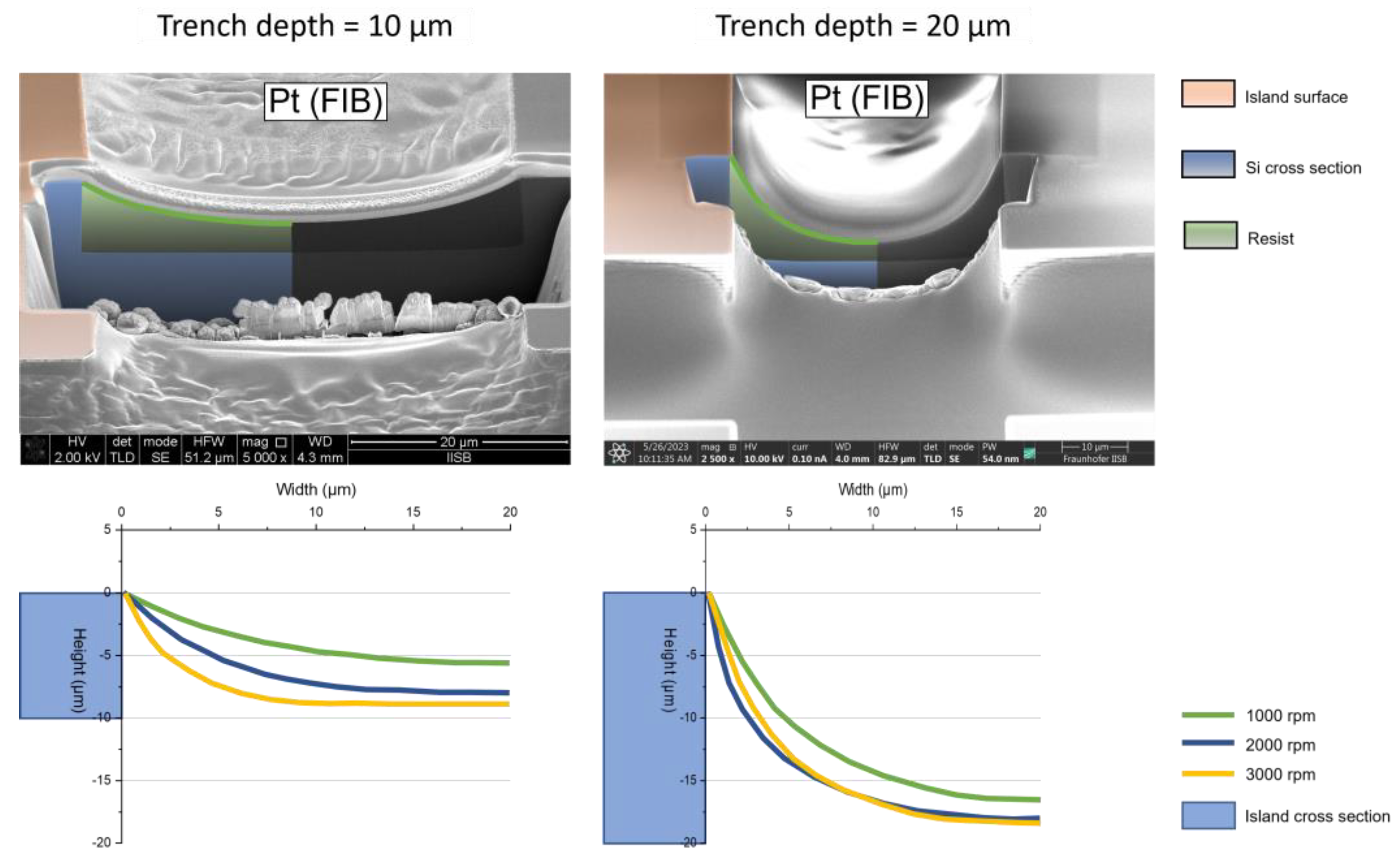
For the filling of the trenches with resist it is investigated at which speed during spin coating the arc shape structure is achieved in the trenches. This is done for the 10 µm deep trenches as well as for the 20 µm depth. Figure 6 shows two examples of a cross section in the trench with depth of 10 and 20 µm. The green line represents the profile of the resist, which is equal to the final form of the metal bridge. The profile for each spin speed is extracted for both trench depths. The diagrams in
Figure 6 show the results. With increasing the spin speed, the resist gets thinner in the middle of the trench, which means, that the penetration depth for the metal bridge gets increased. The largest difference in both trenches is between 1000 and 2000 rpm, while the depth for 2000 and 3000 rpm is almost the same. For a trench depth of 10 µm it can clearly be seen that with 3000 rpm the resist forms a plateau. In the 20 µm deep trench this also seems to start with the 2000 and 3000 rpm. The aim for the final process is to get a well-formed arc shape, so for producing the final metal bridges the parameters are set to 1000 and 2000 rpm for the 10 µm trench and to 1000 rpm for the 20 µm. Care must be taken about the wetting of the trench walls with resist. This gets particularly significant for the trench depth of 20 µm. In the corresponding FIB image, the edge of the island is not covered. This is important for the layout of the bridges, meaning that the structures should be placed in the center of island and trench.
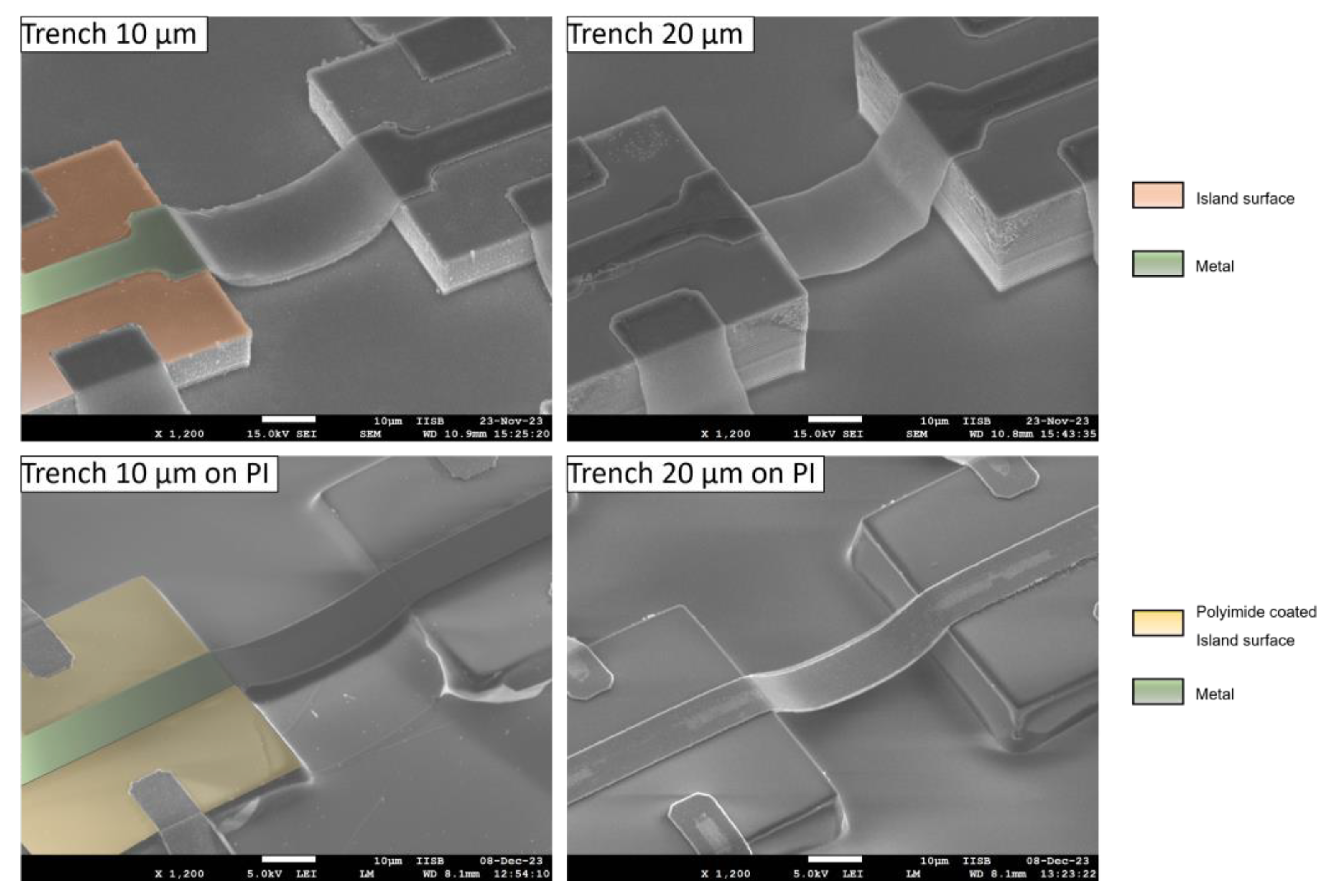
In a next step the freestanding metal bridges are formed on top of the resist coating. As described in section 2.2 the structures are formed on a bare silicon surface and on Polyimide coated islands, which would be the final application. The results can be seen in
Figure 7. The lithography and the structuring itself worked for a trench depth of 10 and 20 µm. On a bare silicon surface with the 20 µm deep trench the bridge is no longer quite as well formed as an arc shape, but the bridge penetrates quite well into the depth, which is also achieved for the 10 µm deep trench. Regarding the trench depth it can be seen that with a PI coating it is significantly reduced. As with the simulations described the trench depth is the key factor for generating more strain in the structures. So, the PI filling must be taken into account as a design parameter for the trench depth meaning that the trenches must be over etched for getting a specific trench depth in the final substrate.
3.3. Conductivity Measurements
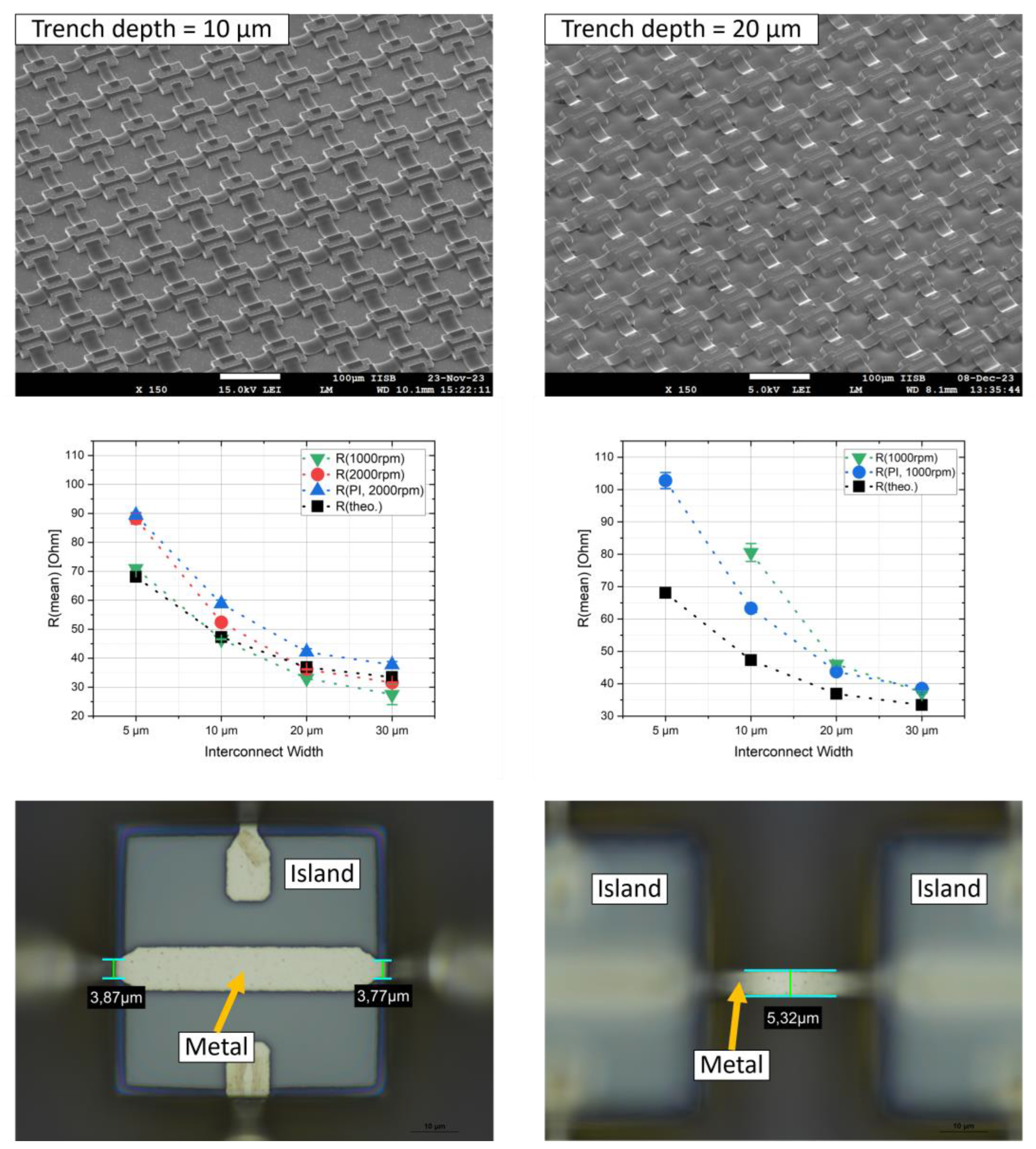
To verify the functionality of the bridges the fabricated island-bridge arrays are electrically characterized using I-V measurements and a mean value of resistance for each metal width is determined. The results are compared to the theoretical resistance. Examples for the arrays and the results of the functionality test can be seen in
Figure 8. The theoretical values show a decrease of the resistance with increasing the width of the metal. This can also be seen for all measured structures. For the trenches with 10 µm depth the results are quite close to the theoretical values, especially the trench filling with 1000 rpm. There is an offset for the 5 µm width and 2000 rpm for both, the bare silicon (green) surface and the PI coated (blue) one. For the 20 µm deep trenches the results for the 5 and 10 µm width are broader distributed and for the bare silicon surface no value for the 5 µm width could be determined, because no current flow could be detected. These bridges over the 20 µm deep trenches are the most critical structures in this process. After structuring the metal, it can be observed that the structures get thinner at the edge of the island, meaning the width of the metal.
Figure 8, bottom row, shows two examples. This causes an increase of the resistance and is very susceptible to defects. For the PI coated islands this effect gets less and the structure width of 5 µm over a 20 µm deep trench are ok, but a larger difference to the theoretical resistance can be seen. As described the PI decreases the trench depth and makes the edge of the silicon island smoother. Both can help avoiding defects in the metal bridges.
4. Conclusions
Based on numerical modelling, we have successfully demonstrated an optimized manufacturing route for flexible interconnects, which uses the trench depth as a design parameter which can be completely integrated into the standard silicon planar technology. Detailed investigations on the trench depth simulations clearly showed that with increasing the slope of the metal bridge when reaching the island more tensile load is converted into the shear force Q(x). This effect improves the overall stress distribution during tensile load.
To implement this structure in a manufacturing process, the filling of the trenches with resist works well over a complete island-bridge array with a size of 0.5 x 0.5 cm. While both trench depth can be filled with 1000 rpm during spin coating, the filling with 2000 rpm leads to even better arc shape structures in the 10 µm deep trench.
Current-voltage measurements show a decrease of resistance with increasing the width, which fits the estimated theoretical resistance values. Although, some deviations in the practical measured values to the theoretical ones can be expected, it must be emphasized that all metal interconnects on the final PI coated wafers are found to be completely operational demonstrating the scalability of this approach.
Author Contributions
Conceptualization, Daniel Joch; Data curation, Daniel Joch; Formal analysis, Daniel Joch and Thomas Lang; Investigation, Daniel Joch and Thomas Lang; Methodology, Daniel Joch; Resources, Daniel Joch; Software, Daniel Joch; Supervision, Michael Jank; Writing – original draft, Daniel Joch; Writing – review & editing, Daniel Joch, Shawn Sanctis and Michael Jank. All authors will be informed about each step of manuscript processing including submission, revision, revision reminder, etc. via emails from our system or assigned Assistant Editor.
Funding
This research received no external funding
Institutional Review Board Statement
Not applicable.
Informed Consent Statement
Not applicable.
Data Availability Statement
Data are contained within the article.
Acknowledgments
This work was supported by the Fraunhofer Internal Programs under Grant No. MAVO 840 092.
Conflicts of Interest
The authors declare no conflict of interest.
Appendix A
Here, the derivation for the equations from section 3.1 are shown. The following calculations are based on [12] and [14].
With the assumption of an uniform surface load there is the general differential equation of 4th order [
12,
14]:
Here, E is the young’s modulus, I the geometrical moment of inertia, w the curvature and q the surface load. The x coordinate describes a specific point along the beam and is in the range of 0 ≤ x ≤ l, where l is the maximum length of the beam. Integrating equation 4 leads to the four constants:
The constants can be solved with the boundary condition that the beam is clamped at both ends [12]:
With the second derivation of equation (6) the bending moment M(x) can be calculated [
12,
14]:
And with the derivation of M(x) the shear force Q(x) can be calculated:
As described in our results the most critical point for the stress in the metal is the point next to the edge of the island. And we mentioned that the stress should not overcome the yield strength γs.
When using γs as σx in equation 1 from section 3.1 there is a second possibility to calculate M(x). After that M(x) and equation 7 can be used to get q(x), which is needed in equation 8 for Q(x).
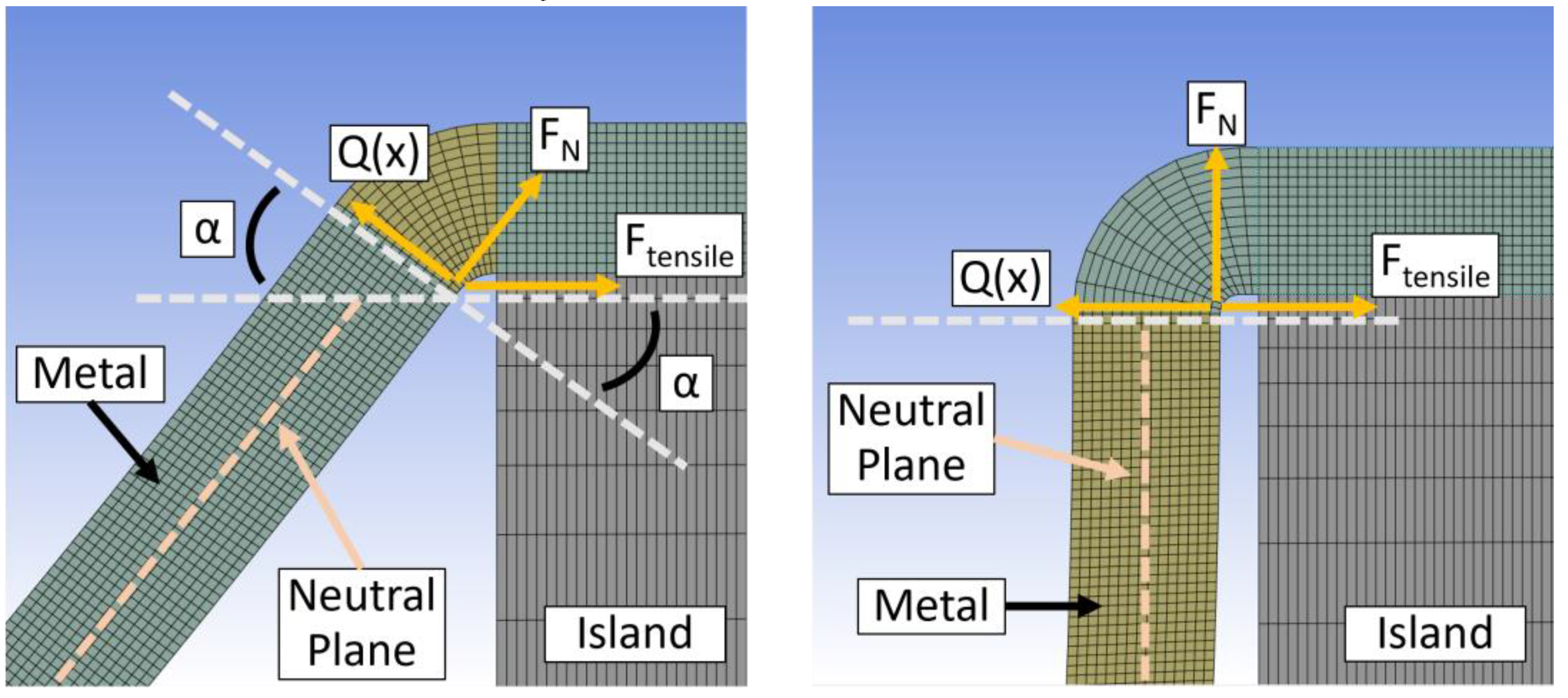
When Q(x) is solved in this way the correlation of forces can be drafted as can be seen in
Figure 9.
Figure 9.
Description of correlation of forces at the critical point at the end of the metal bridge: Example for a bridge through a 40 µm long a 10 µm deep trench (left), trench with width = 40 µm and height = 20 µm (right).
Figure 9.
Description of correlation of forces at the critical point at the end of the metal bridge: Example for a bridge through a 40 µm long a 10 µm deep trench (left), trench with width = 40 µm and height = 20 µm (right).
There are the shear force Q(x) and the normal force F
N, which come from the bending of the structure [12]. The third one is the tensile force F
tensile, because of the deformation in x direction. Finally, to get F
tensile the standard trigonometric functions can be used. Therefore, the angular α must be determined from the model by measuring it during the building of the model. As illustrated in
Figure 9 the angular α decreases with increasing the slope of the metal bridge. For the 20 µm deep trench (
Figure 9, right) it can be assumed as 0. So, F
tensile can be calculated for every geometry variation and be used for the simulations.
References
- J. L. a. J. W. Lu Yin, „Structural Innovations in Printed, Flexible, and Stretchable Electronics”, Advanced Materials Technology, Bd. 5, Nr. 11, p. 2000694, 2020.
- X. C. Z. B. a. T. S. Naoji Matsuhisa, „Materials and structural designs of stretchable conductors”, Chemical Society Reviews, Bd. 48, pp. 2946-2966, 2019. [CrossRef]
- H. S. J. A. R. Y. Z. a. Y. H. Zhaoguo Xue, „Mechanically-Guided Structural Designs in Stretchable Inorganic Electronics”, Advanced Materials, Bd. 32, Nr. 15, p. 1902254, 2020. [CrossRef]
- Y. M. a. Y. H. Haibo Li, „Material innovation and mechanics design for substrates and encapsulation of flexible electronics: a review”, Material Horizons, Bd. 8, pp. 383-400, 2021. [CrossRef]
- J. S. W. M. C. H.-S. K. R.-H. K. Z. L. Y. Y. H. K.-C. H. Y.-w. Z. a. J. A. R. Dae-Hyeong Kim, „Materials and noncoplanar mesh designs for integrated circuits with linear elastic responses to extreme mechanical deformations”, PNAS, Bd. 105, Nr. 48, pp. 18675-18680, 2008. [CrossRef]
- J. W., J. H. R., Z. L., M. M., Y.-W. Z. Y. H., a. J. A. R. Jongho Lee, „Stretchable Semiconductor Technologies with High Areal Coverages and Strain-Limiting Behavior: Demonstration in High-Effi ciency Dual-Junction GaInP/GaAs Photovoltaics”, small, Bd. 8, Nr. 12, pp. 1851-1856, 2012. [CrossRef]
- T. Z. M. B. L. W. K. J. L. E. S. Sosin, „Mesh Interconnects for Silicone Embedded Stretchable Silicon Electronics”, 10th Electronics Packaging Technology Conference (EPTC), pp. 230-235, 2008.
- V. H. A. v. d. H. a. R. D. Benjamin Mimoun, „Flex-to-Rigid (F2R): A Generic Platform for the Fabrication and Assembly of Flexible Sensors for Minimally Invasive Instruments”, IEEE Sensors Journal, Bd. 13, Nr. 10, pp. 3873-3882, 2013.
- J. P. M. H. A. S. S. J. R. D. a. M. G. D. G. Salman Shafqat, „Ultra-Stretchable Interconnects for High-Density Stretchable Electronics”, MDPI micromachines, Bd. 8, Nr. 277, 2017. [CrossRef]
- T. L. S. S. a. M. P. M. J. Daniel Joch, "STRETCH-FREE, SHAPE-INDUCED INTERCONNECTS FOR FLEXIBLE ELECTRONICS VIA AN ISLAND-BRIDGE FABRICATION PROCESS," 20th International Conference on Experimental Mechanics, no. 19908, 2023.
- J. R. R. (Ed.), „Electrical Resistivity of Pure Elemental Metals as a Function of Temperature”, in CRC Handbook of Chemistry and Physics, 103rd Edition (Internet Version 2022), FL, USA, RC Press/Taylor & Francis: Boca Raton, 2022.
- M. S. H. A. Richard, „Biegung von Balken und balkenartigen Tragwerken,“ in Technische Mechanik. Festigkeitslehre, Vieweg+Teubner, 2008, pp. 56-108.
- S. J. B. A. O. A. G. O. N. W. A. H. a. J. d. S. S. Soare, "Determination of mechanical parameters for rotating MEMS structures as a function of deposition method," MRS Online Proceedings Library, Vols. 795: Symposium U - Thin Films - Stresses and Mechanical Properties X, no. U9.2, 2003.
- H. Balke, „Kapitel 4 - Reine Biegung gerader Balken,“ in Einführung in die Technische Mechanik, Berlin Heidelberg, Springer Verlag, 2010, pp. 79-130.
|
Disclaimer/Publisher’s Note: The statements, opinions and data contained in all publications are solely those of the individual author(s) and contributor(s) and not of MDPI and/or the editor(s). MDPI and/or the editor(s) disclaim responsibility for any injury to people or property resulting from any ideas, methods, instructions or products referred to in the content. |
© 2024 by the authors. Licensee MDPI, Basel, Switzerland. This article is an open access article distributed under the terms and conditions of the Creative Commons Attribution (CC BY) license (http://creativecommons.org/licenses/by/4.0/).
