Submitted:
25 July 2024
Posted:
26 July 2024
You are already at the latest version
Abstract
Keywords:
1. Introduction
2. The Simulation Model
3. Results and discussion
4. Conclusions
Author Contributions
Data Availability Statement
Conflicts of Interest
Nomenclature
| q | The electrical charge | |
| n | The concentration of free electrons | |
| n0 | The equilibrium density of electron | |
| Nc,v | The effective density of states in the conduction band | |
| p0 | Equilibrium density of holes | |
| P | Concentration of free holes | |
| Jn,p | The current density of the electrons and holes | |
| vth | The thermal emission velocity of the carriers | |
| Ec,v | The conduction and valence band | |
| EF,h,e | The energy corresponding fermi-level | |
| Fn,p | The Fermi level in the conduction and valence band | |
| Dn,p | The diffusion coefficient of the electrons and holes | |
| Rn | The recombination rate of electrons | |
| Rp | The recombination rate of holes | |
| G | The carrier generation rate | |
| KB | Boltzmann constant | |
| T | The Temperature | |
| Greek Symbols | ||
| The permittivity of free space | ||
| Relative permittivity | ||
| φ | The voltage profile | |
| µe,h | Electron and hole mobility | |
| ΔE | The energy offset | |
| ω | The angular frequency of the wave | |
| λ | The wavelength | |
| Superscripts | ||
| D | Electron donor | |
| A | Electron Acceptor | |
References
- E. D. COYLE and R. A. SIMMONS, Eds., “Introduction,” in Understanding the Global Energy Crisis, Purdue University Press, 2014, pp. 1–8. [Online]. Available: http://www.jstor.org/stable/j.ctt6wq56p.5.
- H. Melin, “Towards a solution to the energy crisis,” Nat Astron, vol. 4, no. 9, pp. 837–838, 2020. [CrossRef]
- D. Mhlanga and E. Ndhlovu, “The Implications of the Russia–Ukraine War on Sustainable Development Goals in Africa,” Fudan Journal of the Humanities and Social Sciences, vol. 16, no. 4, pp. 435–454, 2023. [CrossRef]
- P. F. Borowski, “Mitigating Climate Change and the Development of Green Energy versus a Return to Fossil Fuels Due to the Energy Crisis in 2022,” Energies (Basel), vol. 15, no. 24, 2022. [CrossRef]
- J. A. Burney, “The downstream air pollution impacts of the transition from coal to natural gas in the United States,” Nat Sustain, vol. 3, no. 2, pp. 152–160, 2020. [CrossRef]
- Y. Guan et al., “Burden of the global energy price crisis on households,” Nat Energy, vol. 8, no. 3, pp. 304–316, 2023. [CrossRef]
- F. Creutzig, “Fuel crisis: slash demand in three sectors to protect economies and climate.,” Nature, vol. 606, no. 7914, pp. 460–462, Jun. 2022. [CrossRef]
- Y. Parag, T. Fawcett, S. Hampton, and N. Eyre, “Energy saving in a hurry: A research agenda and guidelines to study European responses to the 2022–2023 energy crisis,” Energy Res Soc Sci, vol. 97, p. 102999, 2023. [CrossRef]
- “The politics of energy security,” Nat Energy, vol. 8, no. 10, p. 1047, 2023. [CrossRef]
- N. Frilingou et al., “Navigating through an energy crisis: Challenges and progress towards electricity decarbonisation, reliability, and affordability in Italy,” Energy Res Soc Sci, vol. 96, p. 102934, 2023. [CrossRef]
- T. Ingram, M. Wieczorek-Kosmala, and K. Hlaváček, “Organizational Resilience as a Response to the Energy Crisis: Systematic Literature Review,” Energies (Basel), vol. 16, no. 2, 2023. [CrossRef]
- J. D. Hunt., D. Stilpen, and M. A. V. de Freitas, “A review of the causes, impacts and solutions for electricity supply crises in Brazil,” Renewable and Sustainable Energy Reviews, vol. 88, pp. 208–222, 2018. [CrossRef]
- D. J. Wuebbles, D. W. Fahey, and K. A. Hibbard, “Climate Science Special Report: Fourth National Climate Assessment, Volume I.” in U.S. National Climate Assessment. United States, 2017. doi: doi: 10.7930/J0J964J6.
- D. Klingelhöfer, R. Müller, M. Braun, D. Brüggmann, and D. A. Groneberg, “Climate change: Does international research fulfill global demands and necessities?,” Environ Sci Eur, vol. 32, no. 1, p. 137, 2020. [CrossRef]
- D. Welsby, J. Price, S. Pye, and P. Ekins, “Unextractable fossil fuels in a 1.5 °C world,” Nature, vol. 597, no. 7875, pp. 230–234, 2021. [CrossRef]
- C. Kroeger, “Heat is associated with short-term increases in household food insecurity in 150 countries and this is mediated by income,” Nat Hum Behav, vol. 7, no. 10, pp. 1777–1786, 2023. [CrossRef]
- C. Guivarch et al., “Using large ensembles of climate change mitigation scenarios for robust insights,” Nat Clim Chang, vol. 12, no. 5, pp. 428–435, 2022. [CrossRef]
- P. Achakulwisut, P. Erickson, C. Guivarch, R. Schaeffer, E. Brutschin, and S. Pye, “Global fossil fuel reduction pathways under different climate mitigation strategies and ambitions,” Nat Commun, vol. 14, no. 1, p. 5425, 2023. [CrossRef]
- C. Kemfert, F. Präger, I. Braunger, F. M. Hoffart, and H. Brauers, “The expansion of natural gas infrastructure puts energy transitions at risk,” Nat Energy, vol. 7, no. 7, pp. 582–587, 2022. [CrossRef]
- V. Masson, M. Bonhomme, J.-L. Salagnac, X. Briottet, and A. Lemonsu, “Solar panels reduce both global warming and urban heat island,” Front Environ Sci, vol. 2, 2014. [CrossRef]
- N. A. Dunne, P. Liu, A. F. A. Elbarghthi, Y. Yang, V. Dvorak, and C. Wen, “Performance evaluation of a solar photovoltaic-thermal (PV/T) air collector system,” Energy Conversion and Management: X, vol. 20, p. 100466, 2023. [CrossRef]
- F. J. M. M. Nijsse et al., “The momentum of the solar energy transition,” Nat Commun, vol. 14, no. 1, p. 6542, 2023. [CrossRef]
- N. Thejo Kalyani and S. J. Dhoble, “Chapter 10 - Empowering the Future With Organic Solar Cell Devices,” in Nanomaterials for Green Energy, B. A. Bhanvase, V. B. Pawade, S. J. Dhoble, S. H. Sonawane, and M. Ashokkumar, Eds., in Micro and Nano Technologies. , Elsevier, 2018, pp. 325–350. [CrossRef]
- L. X. Chen, “Organic Solar Cells: Recent Progress and Challenges,” ACS Energy Lett, vol. 4, no. 10, pp. 2537–2539, Oct. 2019. [CrossRef]
- D. Lee, J. Kim, G. Park, H. W. Bae, M. An, and J. Y. Kim, “Enhanced Operating Temperature Stability of Organic Solar Cells with Metal Oxide Hole Extraction Layer,” Polymers (Basel), vol. 12, no. 4, 2020. [CrossRef]
- P. Cheng and X. Zhan, “Stability of organic solar cells: challenges and strategies,” Chem. Soc. Rev., vol. 45, no. 9, pp. 2544–2582, 2016. [CrossRef]
- L. Duan and A. Uddin, “Progress in Stability of Organic Solar Cells,” Advanced Science, vol. 7, no. 11, p. 1903259, 2020. [CrossRef]
- W. Yang et al., “Balancing the efficiency, stability, and cost potential for organic solar cells via a new figure of merit,” Joule, vol. 5, no. 5, pp. 1209–1230, 2021. [CrossRef]
- C. Zhang et al., “High-efficiency ternary nonfullerene organic solar cells with record long-term thermal stability,” J. Mater. Chem. A, vol. 8, no. 43, pp. 22907–22917, 2020. [CrossRef]
- X. Xu et al., “Thermally stable, highly efficient, ultraflexible organic photovoltaics,” Proceedings of the National Academy of Sciences, vol. 115, no. 18, pp. 4589–4594, 2018. [CrossRef]
- El Karkri, Z. El Malki, M. Bouachrine, F. Serein-Spirau, and J.-M. Sotiropoulos, “Characterization and simulation study of organic solar cells based on donor–acceptor (D–π–A) molecular materials,” RSC Adv., vol. 10, no. 32, pp. 18816–18823, 2020. [CrossRef]
- M. R. Khan and B. Jarząbek, “Optimization and Efficiency Enhancement of Modified Polymer Solar Cells,” Aug. 2023. [CrossRef]
- C. Anrango-Camacho, K. Pavón-Ipiales, B. A. Frontana-Uribe, and A. Palma-Cando, “Recent Advances in Hole-Transporting Layers for Organic Solar Cells,” Nanomaterials, vol. 12, no. 3, 2022. [CrossRef]
- H. Tang et al., “Interface Engineering for Highly Efficient Organic Solar Cells,” Advanced Materials, vol. n/a, no. n/a, p. 2212236. [CrossRef]
- J. Niederhausen, K. A. Mazzio, and R. W. MacQueen, “Inorganicorganic interfaces in hybrid solar cells,” Electronic Structure, vol. 3, no. 3, p. 33002, Sep. 2021. [CrossRef]
- T. Kong, R. Wang, D. Zheng, and J. Yu, “Modification of the SnO2 Electron Transporting Layer by Using Perylene Diimide Derivative for Efficient Organic Solar Cells,” Front Chem, vol. 9, 2021. [CrossRef]
- A. Eliwi et al., “Optimization of SnO2 electron transport layer for efficient planar perovskite solar cells with very low hysteresis,” Mater. Adv., vol. 3, no. 1, pp. 456–466, 2022. [CrossRef]
- “Manual: OghmaNano - Organic and hybrid Material Nano Simulation tool.” Accessed: Dec. 06, 2023. [Online]. Available: https://www.oghma-nano.com/docs.html?page=Manual.
- R. C. I. MacKenzie et al., “Interpreting the Density of States Extracted from Organic Solar Cells Using Transient Photocurrent Measurements,” The Journal of Physical Chemistry C, vol. 117, no. 24, pp. 12407–12414, Jun. 2013. [CrossRef]
- F. Deschler, D. Riedel, B. Ecker, E. von Hauff, E. Da Como, and R. C. I. MacKenzie, “Increasing organic solar cell efficiency with polymer interlayers,” Phys. Chem. Chem. Phys., vol. 15, no. 3, pp. 764–769, 2013. [CrossRef]
- R. C. I. MacKenzie, C. G. Shuttle, M. L. Chabinyc, and J. Nelson, “Extracting Microscopic Device Parameters from Transient Photocurrent Measurements of P3HT:PCBM Solar Cells,” Adv Energy Mater, vol. 2, no. 6, pp. 662–669, 2012. [CrossRef]
- L. Zhu et al., “Single-junction organic solar cells with over 19% efficiency enabled by a refined double-fibril network morphology,” Nat Mater, vol. 21, no. 6, pp. 656–663, 2022. [CrossRef]
- W. Farooq, A. D. Khan, A. D. Khan, and M. Noman, “Enhancing the power conversion efficiency of organic solar cells,” Optik (Stuttg), vol. 208, p. 164093, 2020. [CrossRef]
| Parameters | Values |
|---|---|
| Electron mobility (μe) Hole mobility (μh) Effective density of free electron (Nc at 300K) Effective density of free hole (Nv at 300K) n to P Recombination rate constant Free carrier statistics Density of states distribution (DoS) Free electron (n) to Trapped electron (strap) Trapped electron (ntrap) to Free hole (P) Trapped Hole (Ptrap) to Free electron (n) Free hole (P) to Trapped hole (Ptrap) Number of traps (Nt) Energy bandgap (Eg) Relative permittivity (Ɛr) |
1.49e-07 m-2V-1s-1 1.42e-07 m-2V-1s-1 1e26 m-3 1e26 m-3 1.15e-17 m-3s-1 Maxwell Boltzmann-numerical + analysis Complex 1e-15 m-2 1e-20 m-2 1e-20 m-2 1e-15 m-2 5 Trap 1.29 eV 3.0 a.u |
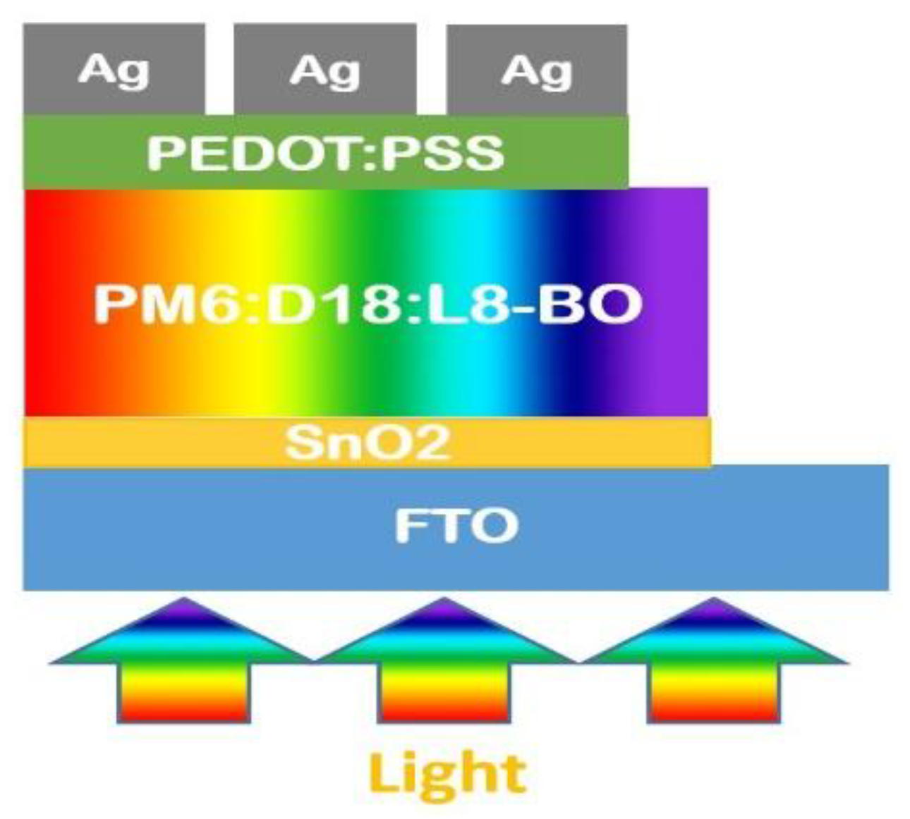
| Layer | Thickness (nm) | Materials | Type |
|---|---|---|---|
| ITO | 130 | Oxides | Contact |
| SnO2 | 5 | Polymers | Other |
| PM6:D18:L8-BO | 80 | Blends | Active |
| PEDOT: PSS | 20 | Oxides | Other |
| Ag | 100 | Metal | Contact |
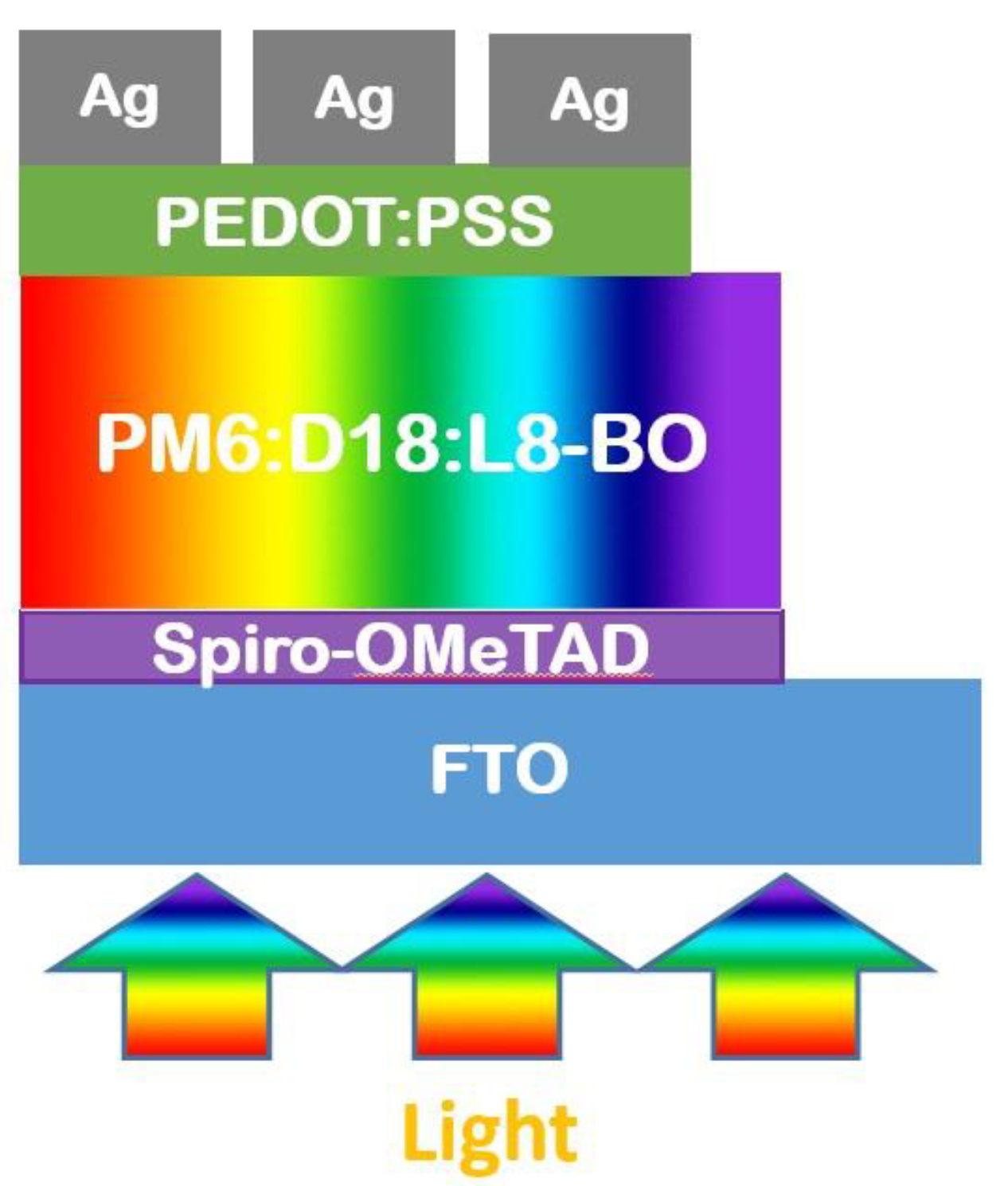
| Layer | Thickness (nm) | Materials | Type |
|---|---|---|---|
| ITO | 130 | Oxides | Contact |
| Spiro-OMeTAD | 5 | Polymers | Other |
| PM6:D18:L8-BO | 80 | Blends | Active |
| PEDOT: PSS | 20 | Oxides | Other |
| Ag | 100 | Metal | Contact |
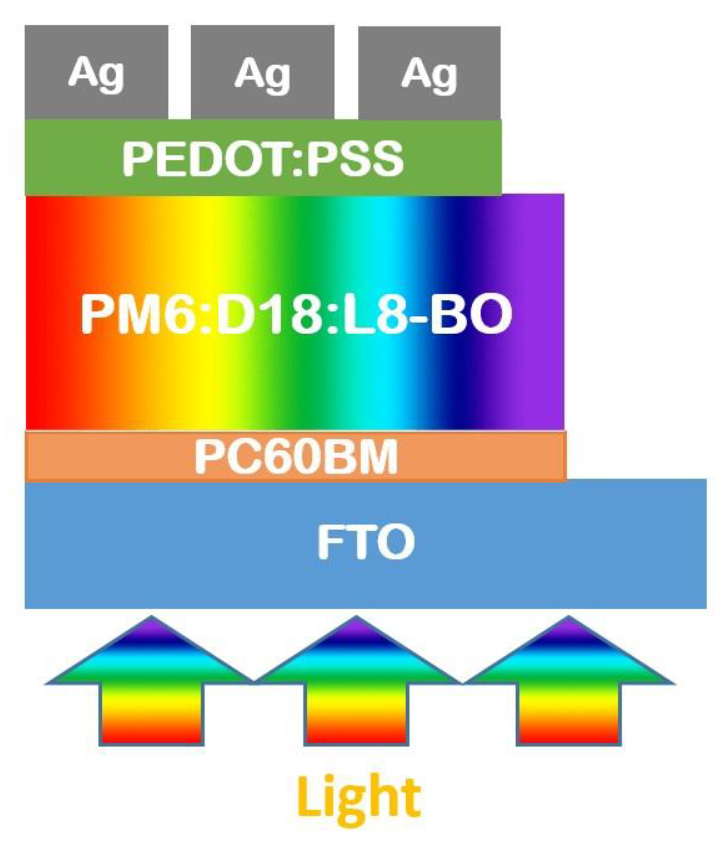
| Layer | Thickness (nm) | Materials | Type |
|---|---|---|---|
| ITO | 130 | Oxides | Contact |
| PC60BM | 5 | Polymers | Other |
| PM6:D18:L8-BO | 80 | Blends | Active |
| PEDOT: PSS | 20 | Oxides | Other |
| Ag | 100 | Metal | Contact |
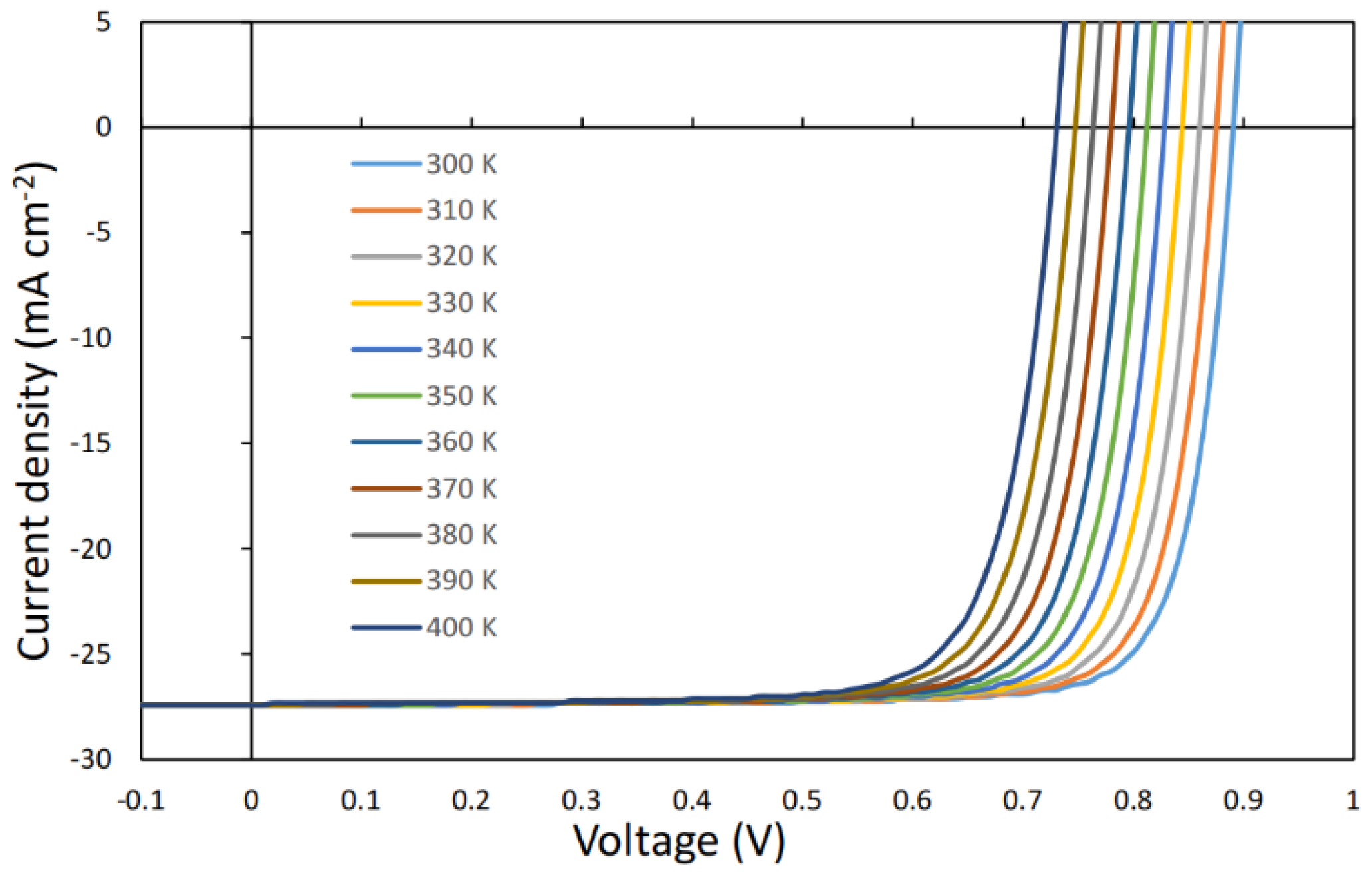
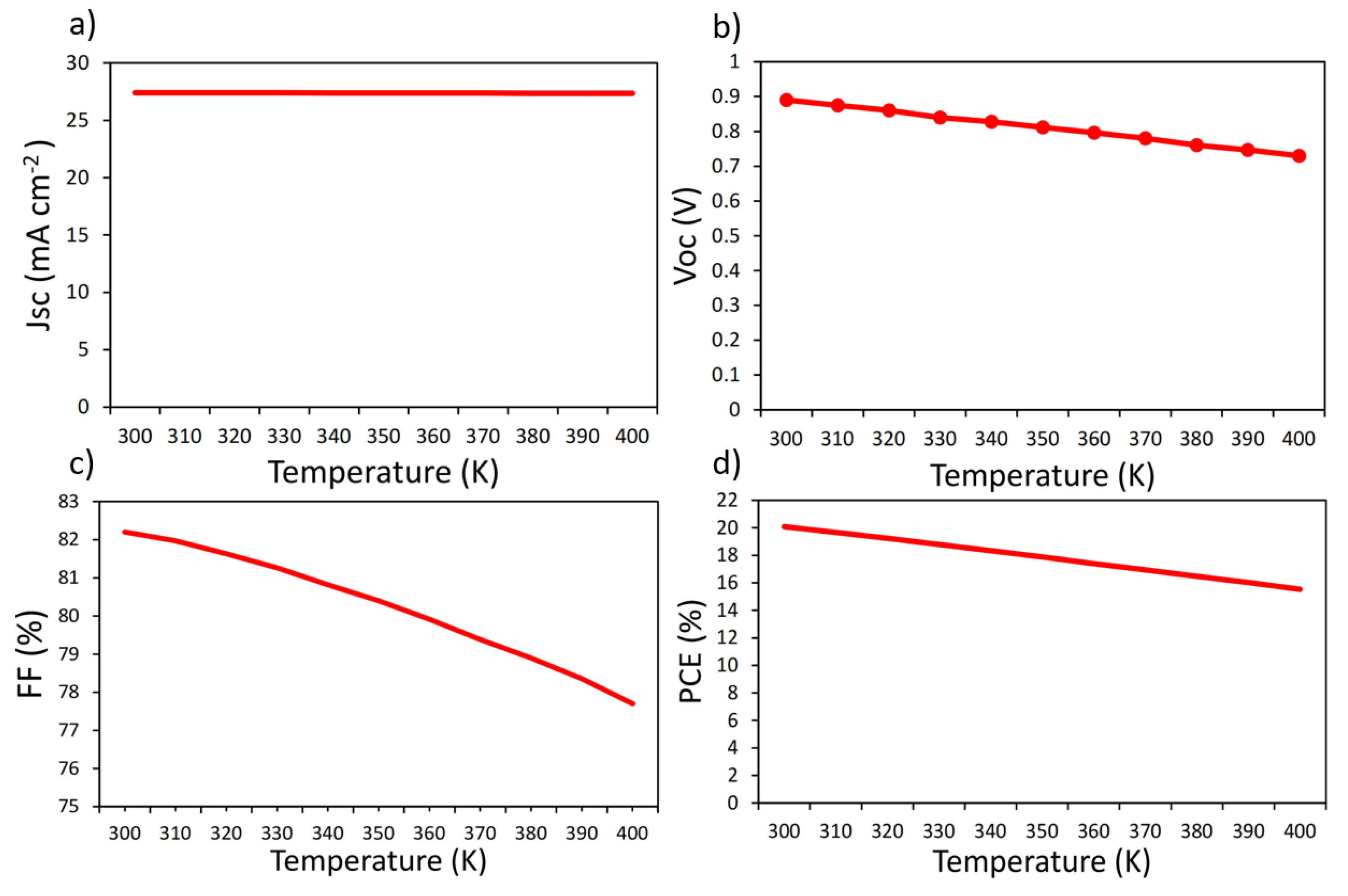
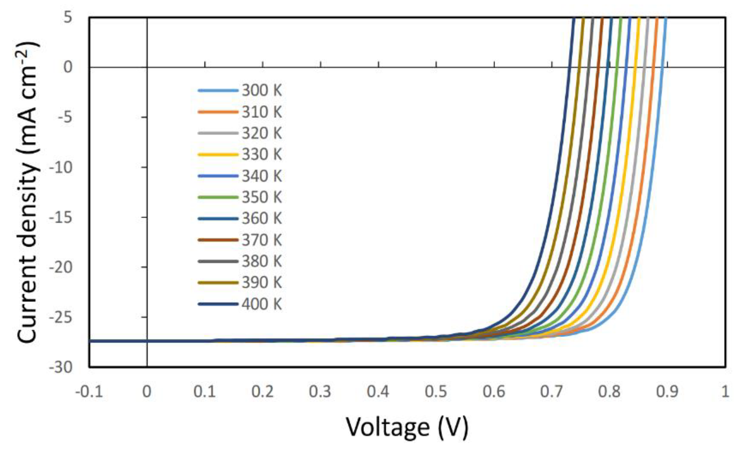
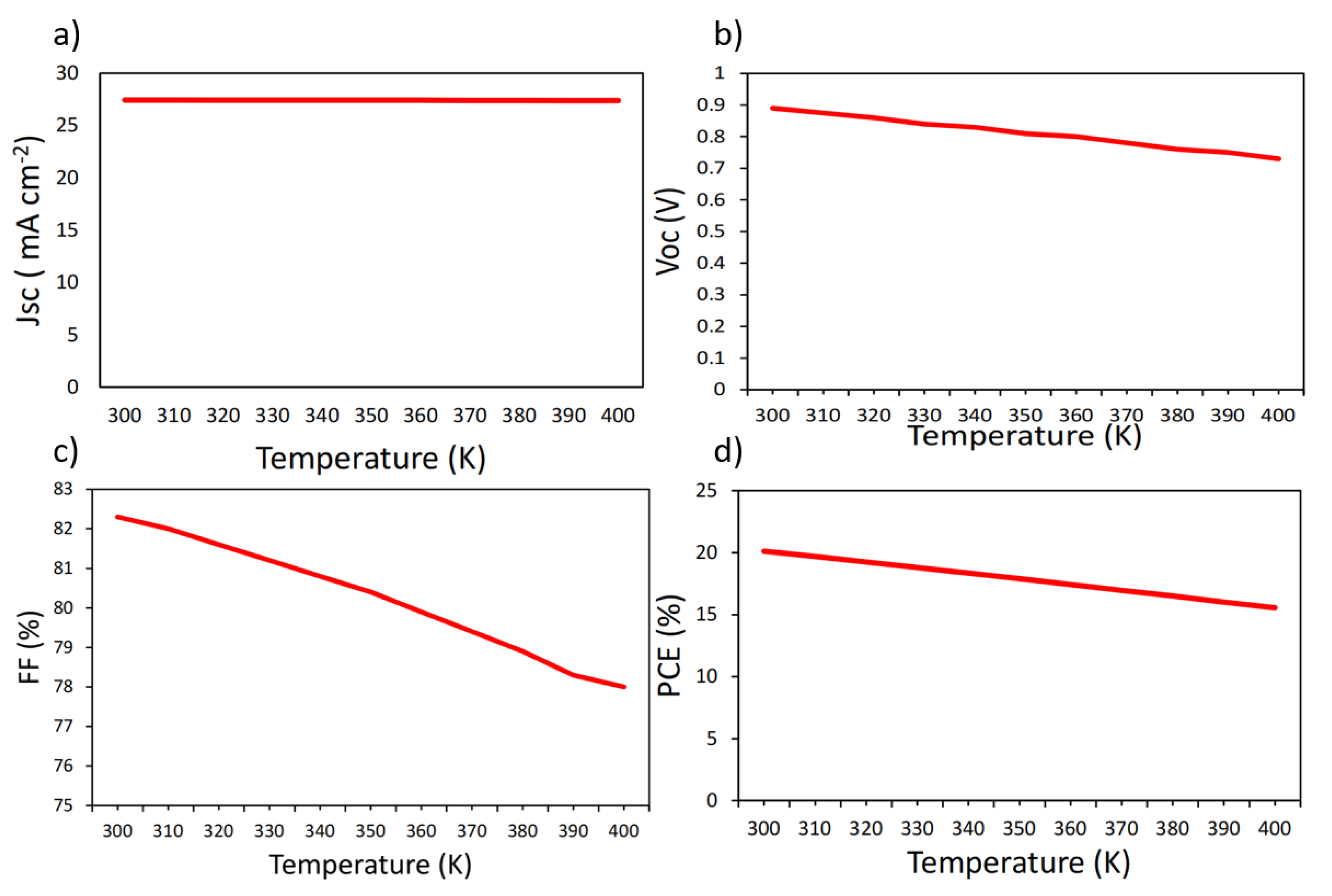
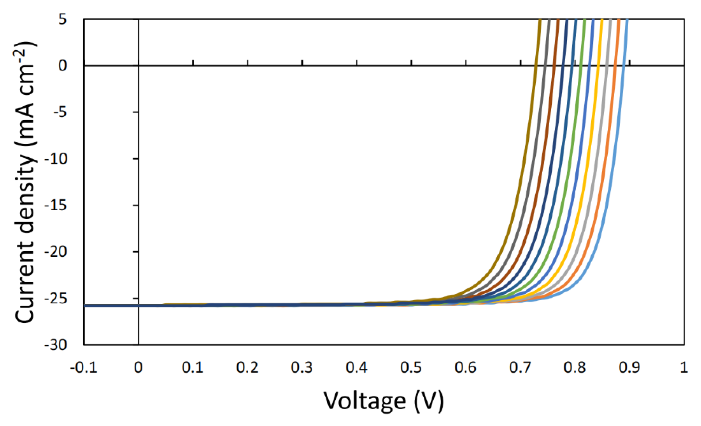
| T(K) | T(°C) | Jsc(mA cm-2) | Voc(V) | FF(%) | PCE(%) | |
|---|---|---|---|---|---|---|
| S1 | 300 | 26.85 | 27.4 | 0.89 | 82.2 | 20.08 |
| 310 | 36.85 | 27.4 | 0.875 | 81.97 | 19.66 | |
| 320 | 46.85 | 27.4 | 0.86 | 81.63 | 19.23 | |
| 330 | 56.85 | 27.4 | 0.84 | 81.26 | 18.78 | |
| 340 | 66.85 | 27.38 | 0.828 | 80.82 | 18.33 | |
| 350 | 76.85 | 27.38 | 0.812 | 80.4 | 17.88 | |
| 360 | 86.85 | 27.37 | 0.796 | 79.91 | 17.4 | |
| 370 | 96.85 | 27.37 | 0.78 | 79.38 | 16.95 | |
| 380 | 106.85 | 27.36 | 0.76 | 78.9 | 16.48 | |
| 390 | 116.85 | 27.36 | 0.747 | 78.35 | 16.01 | |
| 400 | 126.85 | 27.35 | 0.73 | 77.7 | 15.53 | |
| S2 | 300 | 26.85 | 27.43 | 0.89 | 82.3 | 20.11 |
| 310 | 36.85 | 27.43 | 0.875 | 82 | 19.68 | |
| 320 | 46.85 | 27.42 | 0.86 | 81.6 | 19.25 | |
| 330 | 56.85 | 27.42 | 0.84 | 81.2 | 18.8 | |
| 340 | 66.85 | 27.41 | 0.83 | 80.8 | 18.35 | |
| 350 | 76.85 | 27.41 | 0.81 | 80.4 | 17.9 | |
| 360 | 86.85 | 27.41 | 0.8 | 79.9 | 17.43 | |
| 370 | 96.85 | 27.4 | 0.78 | 79.4 | 16.96 | |
| 380 | 106.85 | 27.4 | 0.76 | 78.9 | 16.5 | |
| 390 | 116.85 | 27.38 | 0.75 | 78.3 | 16 | |
| 400 | 126.85 | 27.38 | 0.73 | 78 | 15.55 | |
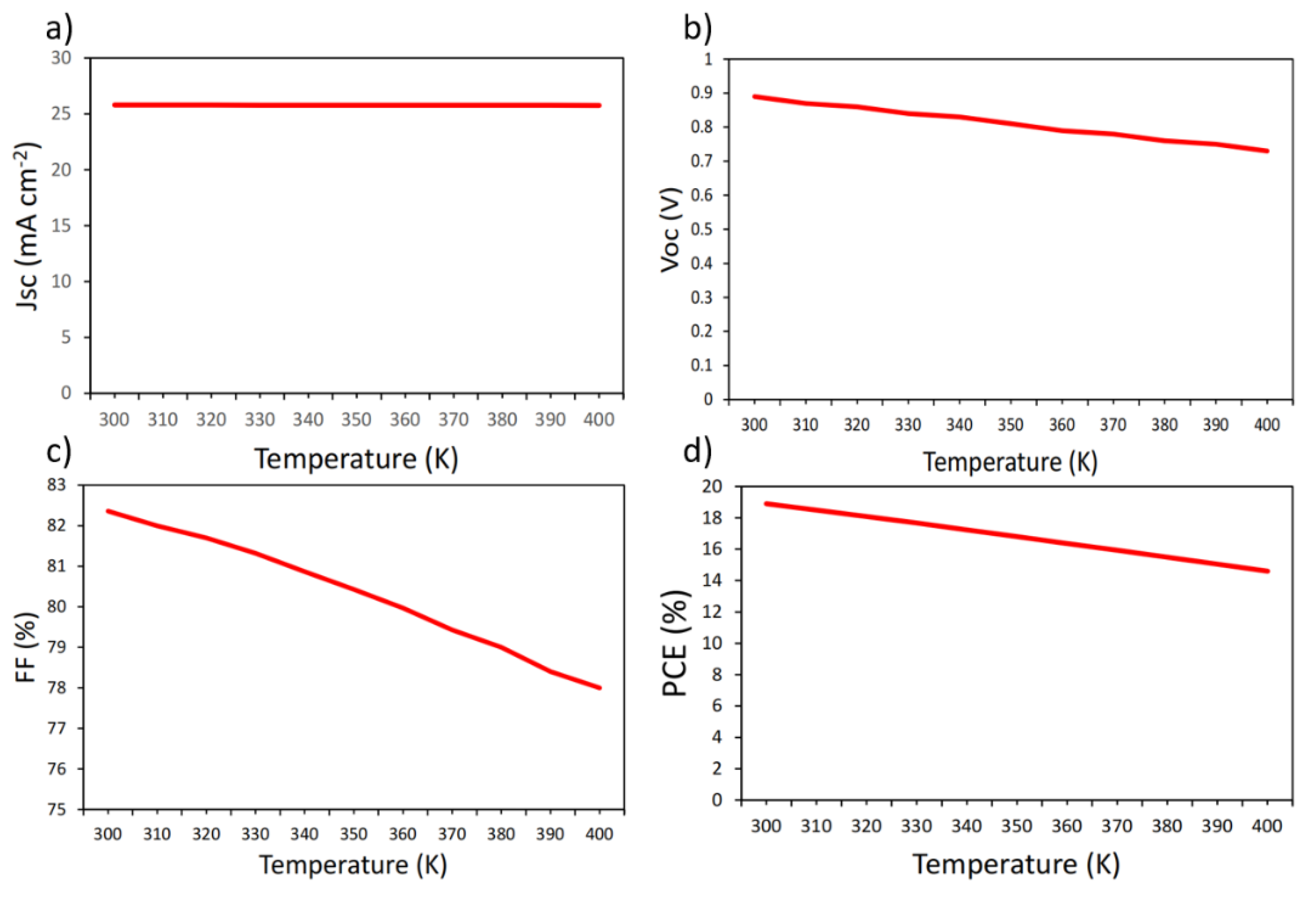
| S3 | 300 | 26.85 | 25.8 | 0.89 | 82.36 | 18.9 |
| 310 | 36.85 | 25.8 | 0.87 | 82 | 18.5 | |
| 320 | 46.85 | 25.8 | 0.86 | 81.7 | 18.08 | |
| 330 | 56.85 | 25.79 | 0.84 | 81.32 | 17.67 | |
| 340 | 66.85 | 25.79 | 0.83 | 80.87 | 17.23 | |
| 350 | 76.85 | 25.78 | 0.81 | 80.43 | 16.81 | |
| 360 | 86.85 | 25.78 | 0.79 | 79.97 | 16.37 | |
| 370 | 96.85 | 25.77 | 0.78 | 79.43 | 15.93 | |
| 380 | 106.85 | 25.77 | 0.76 | 79 | 15.5 | |
| 390 | 116.85 | 25.77 | 0.75 | 78.4 | 15.05 | |
| 400 | 126.85 | 25.76 | 0.73 | 78 | 14.6 |
Disclaimer/Publisher’s Note: The statements, opinions and data contained in all publications are solely those of the individual author(s) and contributor(s) and not of MDPI and/or the editor(s). MDPI and/or the editor(s) disclaim responsibility for any injury to people or property resulting from any ideas, methods, instructions or products referred to in the content. |
© 2024 by the authors. Licensee MDPI, Basel, Switzerland. This article is an open access article distributed under the terms and conditions of the Creative Commons Attribution (CC BY) license (http://creativecommons.org/licenses/by/4.0/).


