1. Introduction
The Transient Current Technique (TCT) is a tool for the characterisation and investigation of detector technologies [
1]. Excess charge carriers are generated via laser light inside the device under test (DUT) and the excess carrier’s drift is studied to obtain information about the DUT. TCT is widely used for the characterisation of silicon detectors that are used within high energy physics experiments [
2,
3]. Conventional TCT uses red or near infrared light to generate excess charge carriers in silicon. The number of charge carriers created at these wavelengths grows linearly with the light intensity. Compared to conventional TCT, the Two Photon Absorption - Transient Current Technique (TPA-TCT) uses light in the quadratic absorption regime (here
) to generate excess charge by two photon absorption (TPA) [
4]. The generation of excess charge carriers by TPA depends quadratically on the light intensity, which is why focused laser light dominantly generates excess charge in a small volume (here about
) around the focal spot. Thus, TPA-TCT enables device characterisation with three-dimensional spatial resolution [
5]. The technique was developed in the framework of the RD50 collaboration [
6,
7] and a table-top setup for the characterisation of silicon detectors was commissioned at CERN [
8]. The development of radiation hard detectors for future detector technologies requires suitable characterisation techniques to obtain a profound understanding about the devices, before and after irradiation. The potential of the TPA-TCT as a characterisation tool was already demonstrated in non-irradiated devices [
9], but besides few studies in irradiated devices [
10,
11], a systematic investigation of the TPA-TCT in irradiated devices for different particle types was so far never reported. This paper is dedicated to such a systematic investigation of the influence of neutron, proton, and gamma irradiation of different fluences and doses on the TPA-TCT. The reported measurements were conducted and published within a broader framework in a PhD thesis [
12].
2. Experimental Setup
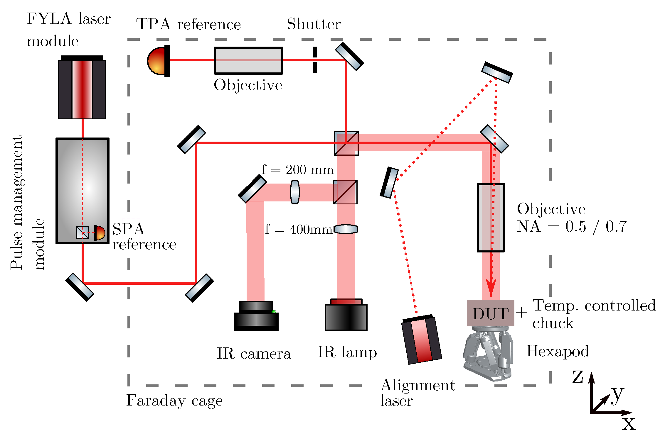
For the here presented study, a table-top TPA-TCT setup is used, which is shown as a schematic in
Figure 1.
The FYLA LFC1500X fibre laser module is used as a laser source [
13]. The central wavelength is
, the temporal pulse width is about
, the output pulse frequency is
, and the pulse energy is
at its output. Downstream the output, the light is guided in a pulse management module, where an acusto-optic modulator regulates the pulse frequency and a neutral density filter adapts the pulse energy to given values. For the here presented measurements, a pulse frequency of
is used and the laser intensity is scanned between
to
(measured at the position of the DUT). The DUTs are cooled to
during the measurement and the Faraday cage is continuously flushed with dry air to avoid freezing. The beam radius at the waist is
and the Rayleigh length is
. In front of the objective,
of the light is coupled to a second arm by a beam splitter. The second arm is used for the energy reference, where a
thick p-type silicon pad detector serves as a reference for the charge generation by TPA.
The DUTs are glued with silver epoxy to a printed circuit board (PCB), which established the electrical connection. The PCB is mounted below the objective to a copper chuck that is thermally coupled to a Peltier element, where the hot side of the Peltier element is cooled by a HUBER chiller. In order to lower the leakage current of the DUTs, the active cooling to
is performed and the Faraday cage is continuously flushed with dry air. The illumination is applied from the top side into the centre of the opening window of the device. The copper chuck is positioned on a six axes Newport HXP50-MECA stage, which allows high precision movement and rotation along all three dimensional axes. The rotation is used to level the DUT and ensure an orthogonal incidence of the laser. The setup includes an infrared (IR) microscope, with an IR lamp and IR camera. The IR microscope is used to live picture the DUT below the objective and to find regions of interest. Further information about the setup can be found in reference [
4].
The data acquisition is handled by an Agilent DSO9254 oscilloscope, with a bandwidth of
and a sampling rate of
. To obtain induced current signals of a suitable amplitude, the
C2HV transimpedance amplifier from CIVIDEC [
14] is used. It has a bandwidth from
to
.
2.1. Devices
Planar p-type pad silicon detectors are used to investigate the influence of irradiation on the TPA-TCT. Pad detectors are selected, as their simple device design allows to distinguish radiation induced, technique related, and device related effects. The devices were manufactured by CiS [
15] in the campaign CiS16 and information about the devices is summarised in
Table 1. The pad detectors have a circular opening in the top metal with a diameter of
, which is ideal for light based characterisation techniques like the TPA-TCT.
Neutron irradiation was performed at the TRIGA reactor at the Jožef Stefan Institute [
16], proton irradiation at the PS-IRRAD proton facility at CERN [
17], and gamma irradiation at the Ruđer Bošković Institute [
18]. The neutron irradiation in the TRIGA reactor has a broad energy spectrum which is converted by the facility operators into the
equivalent fluence [
19]. This is why
within this work. The notation
is still used to distinguish the type of irradiation from the proton irradiation, where
states the absolute proton fluence. The PS-IRRAD proton facility uses
protons for the irradiation and the hardness factor of the facility is
. The gamma irradiation was performed with a
Co source. No hardness factor can be given for the gamma irradiation due to the completely different damage mechanism. Fluences and doses as well as the annealing states of the devices are included in
Table 1.
3. Influence of Radiation Damage
Radiation damage does not only affect the device performance, but can as well influence the characterisation technique. The influence of radiation damage on the TPA-TCT is systematically studied using a series of irradiated pad detectors. Such a study is needed in order to distinguish technique related from device related effects, which is especially relevant with respect to segmented devices.
3.1. Correction of the Single Photon Absorption Offset
Defects can introduce energy levels within the band gap of silicon, which lead to additional linear absorption [
20]. This additional single photon absorption contribution is called single photon absorption (SPA) background or SPA offset. The SPA background is independent of the focal point’s position and appears as a constant offset in a charge collection scan. Three different methods to correct the SPA offset are available: correction by subtraction [
11], correction by intensity [
8], and correction by waveform subtraction [
5]. The prior is the simplest method, where a constant is fitted to the offset and subtracted from the charge profile. It does not provide a correction on the waveform level, which means that is does not correct the influence of the SPA contribution towards the shape of the current transient. Due to its simplicity it is useful to correct collected charge (CC) profiles, but it is not applicable to correct e.g. the prompt current or the time over threshold (ToT). The intensity method requires the measurement to be recorded twice at different laser intensities. For the correction, it is exploited that the SPA and the TPA contribution scale differently with the laser intensity. The method was developed to cope with laser beam clipping, as it compares two measurements and thus corrects intrinsically clipping and reflection. Reference [
8] contains more information about the method and derives the relevant formulas. The third and preferred method is the waveform subtraction method. A waveform is recorded with the focal spot above (i.e. outside of) the active volume. This waveform contains a negligible amount of TPA and is dominated by the SPA contribution. As the SPA contribution is independent on the focal spot’s position, this waveform is subtracted from all other waveforms to cancel out the SPA contribution. The method is only valid if the laser intensity is constant throughout the measurement, i.e. no laser beam clipping or reflection is present.
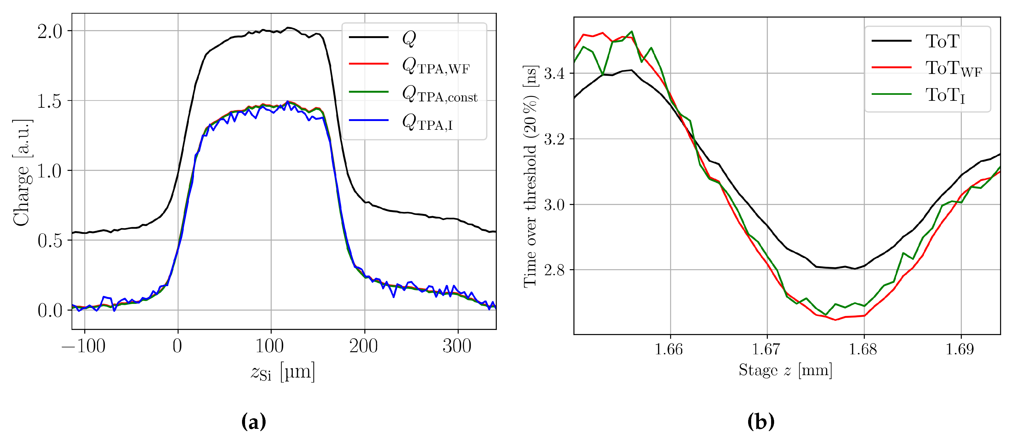
Figure 2 shows a comparison between the three methods using a neutron irradiated pad detector as an example. The correction of the CC profile is shown in (a) and the correction of the ToT profile in (b). Concerning the CC, most striking is the increased noise in the intensity correction method compared to the other methods. This is related to the need to take two measurements at different intensities: in this case one measured at about
and one measured at
. The low intensity measurement has a lower signal-to-noise ratio (SNR), which propagates through the correction method and increases the noise. Such different intensities are needed for the correction method, because too close intensities lead to numerical instability. The subtraction method does not appear in
Figure 2, because it does not provide a correction on the waveform level and thus can not be used to correct the ToT. The waveform subtraction method is the recommended method for SPA correction and used within this work.
3.2. Influence of Neutron and Proton Irradiation
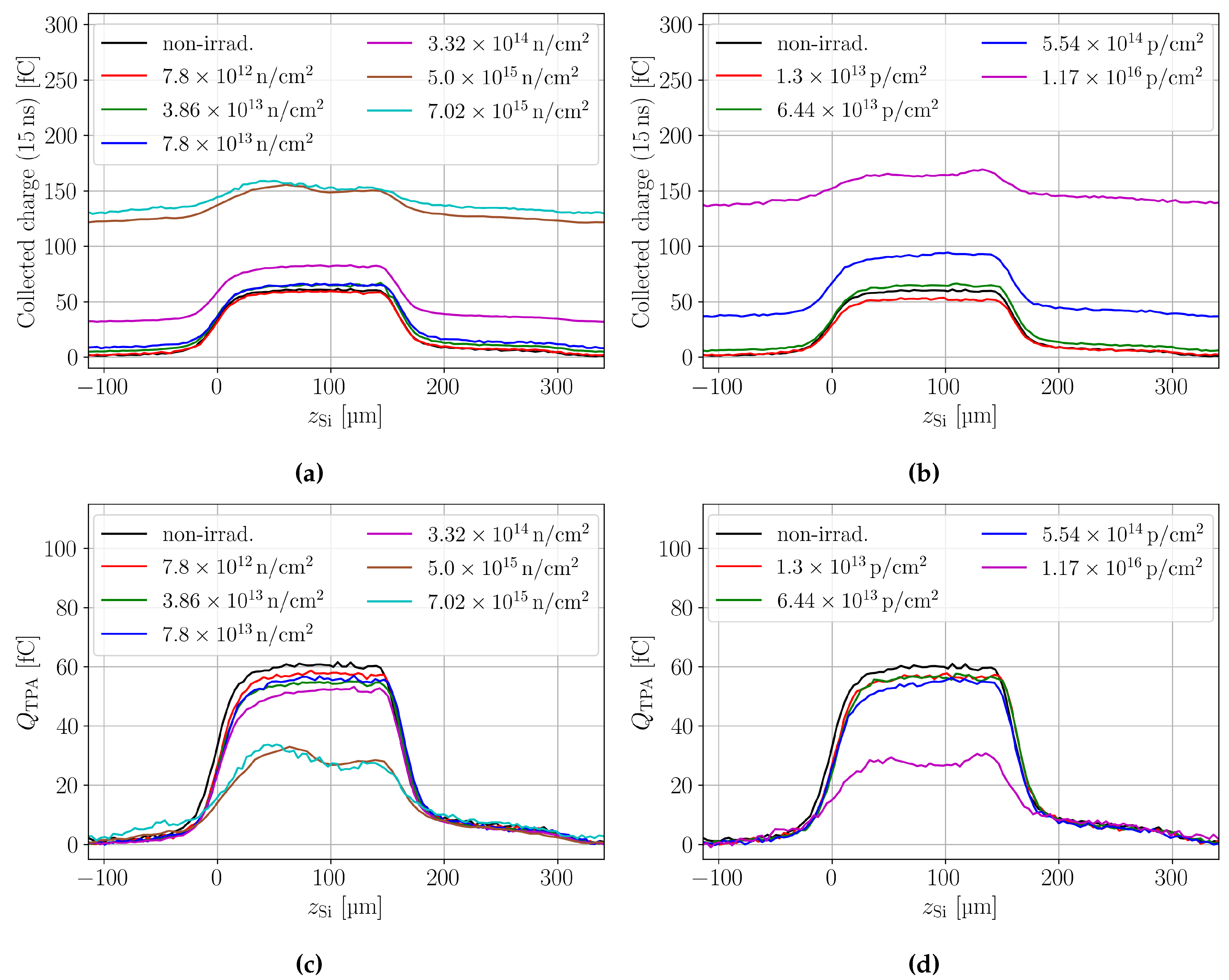
CC profiles of the neutron and proton irradiated samples are shown in
Figure 3 (a) and (b), respectively. It can be seen that both lead to an SPA offset that increases with the fluence. Figures (c) and (d) show the SPA corrected in-depth scans, where the decreasing CC is evident. Further, it can be seen that increasing fluences lead to inhomogeneous CC profiles along the device depth. The inhomogeneity is linked to inhomogeneous electric fields and charge carrier dependent trapping. Depending on the excess charge deposition depth, electrons or holes need to drift a longer distance and face different low field regions, which is why their probability of trapping changes with the deposition depth.
In-depth scans were performed at various bias voltages and laser intensities in order to investigate the linear and quadratic dependence of the SPA and the TPA contribution, respectively. The SPA contribution to the collected charge
is extracted as the mean CC in a range between
in front of the device. In this region, charge generation by TPA can be neglected. The TPA contribution to the collected charge
is extracted from the SPA corrected CC profiles as the mean between the full width at half maximum (FWHM) of the CC profile. It should be noted that the analysis procedure of
can be performed at a given depth of the device to investigate the CC along the device depth. Here, the average over the device depth is used to ease the analysis procedure.
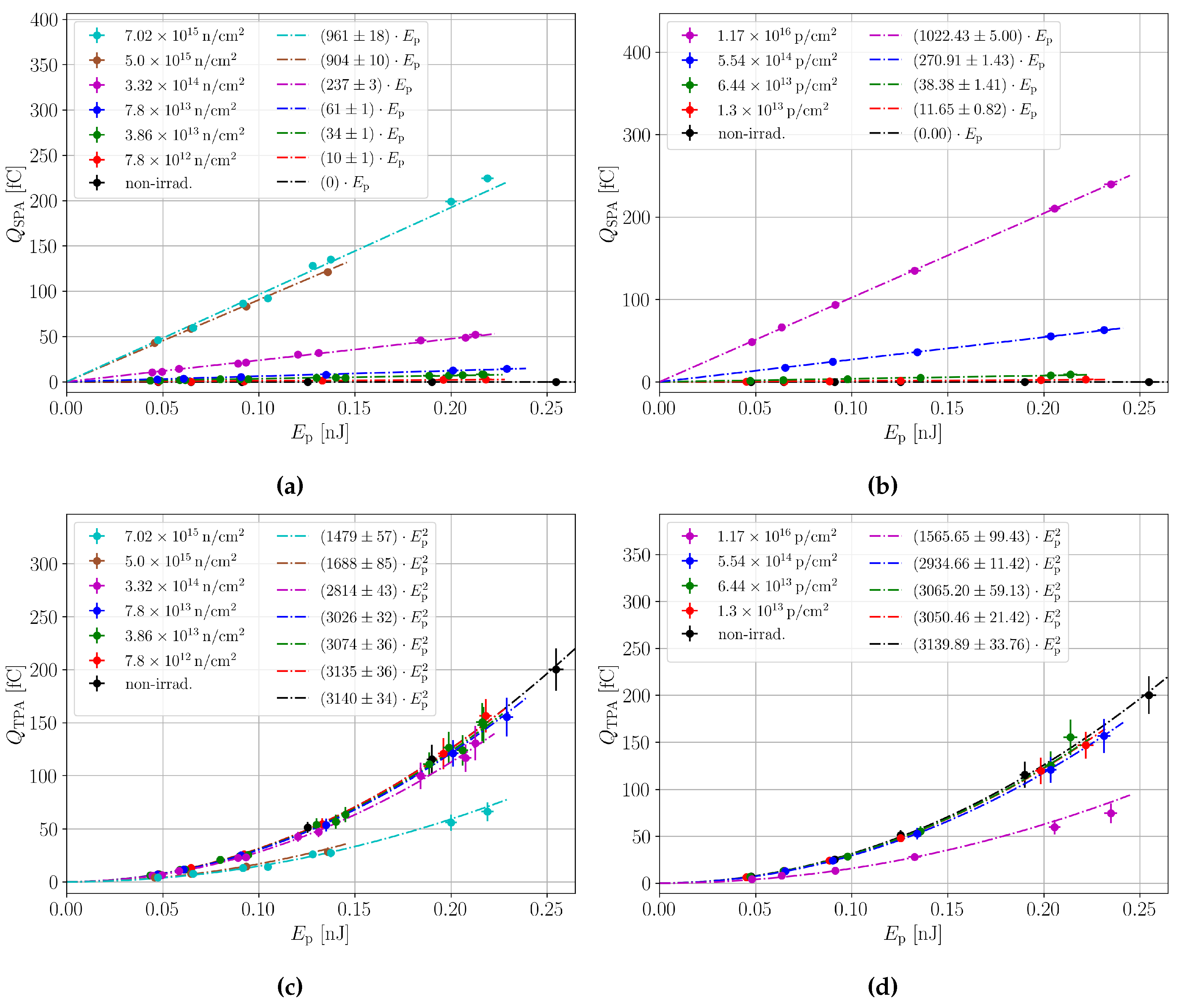
Figure 4 shows the CC from SPA (a) and TPA (c) against the laser intensity. In accordance with the expectations, the SPA contribution scales linearly and the TPA contribution quadratically with the laser intensity. The standard deviation of the averaged SPA and TPA charge yields the corresponding errors on the CC.
The analogous analysis was performed for the proton irradiated samples.
Figure 4 and
Figure 4 show the CC from SPA (b) and TPA (d) against the laser intensity. It can be seen that the proton irradiated samples show a similar behaviour to the neutron irradiated samples. A dedicated comparison between the neutron and proton irradiated samples is performed in
Section 3.4.
The prompt current (PC), i.e. the current measured at
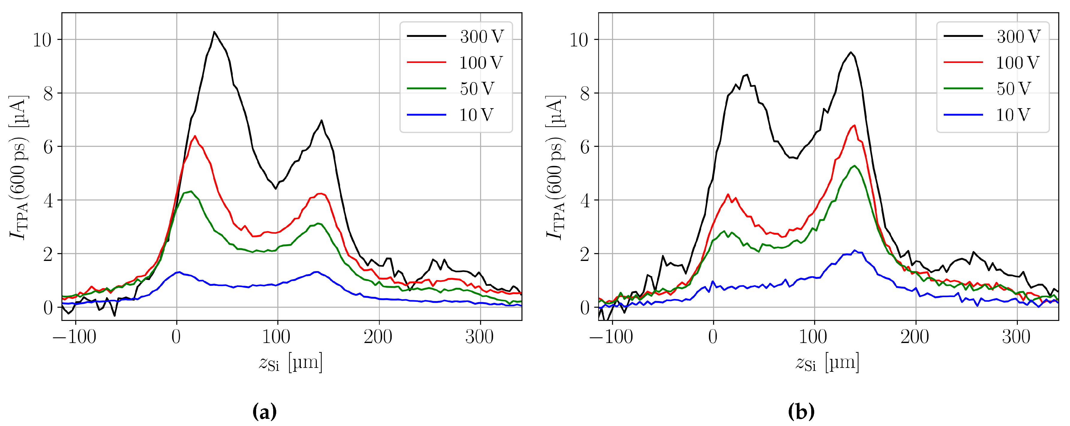
after start of transient, of the highest neutron and proton irradiated sample is shown in
Figure 5 (a) and (b), respectively. The scans were performed at different bias voltages to emphasise the evolution of the electric field. Both samples show a clear double junction effect [
21], as the electric field has maxima at both device boundaries. Further, the direction of electric field evolution is opposite for neutron and proton irradiated devices at the given fluence. While the electric field grows from the top (n
electrode) towards the back side (p
electrode) in the neutron irradiated device, the direction of electric field evolution is opposite in the proton irradiated device. The evolution of electric field from the top towards the back is the typical direction of electric field in a p-type device, while the opposite is the case for n-type devices for which the electric field growth from the (p
electrode). Thus, the space charge of the proton irradiated device appears
sign inverted compared to the neutron irradiated device, which means that in the proton irradiated sensor a higher fraction of the bulk has obtained positive space charge as compared to the neutron irradiated sensor. This is particularly interesting because space charge sign inversion (SCSI) in a p-type FZ detector was so far never reported. However, the situation is complex because of the double junction, which makes the expression of SCSI somewhat ambiguous. The bulk is not fully transitioned from negative to positive space charge as this expression is stating, but contains regions of negative and regions of positive space charge. For the neutron irradiated devices the negative space charge at the n
electrode is higher than the positive space charge at the p
electrode, while the ratio is inverted in the proton irradiated devices.
For pad detectors, the found proton irradiation induced SCSI is not critical, because the weighting field is constant so that excess charge independent of its position contributes equally to the current transient. However, this effect could be significant to p-type strip or pixel detectors. Excess charge in the vicinity of the readout strip has the major contribution the current transient, which is why the highest electric field is desired to be in that region [
22]. Thus, the charge collection efficiency (CCE) of proton irradiated p-type strip detectors might be decreased compared to neutron irradiated devices at high equivalent fluences in segmented sensors.
Besides, from the prompt current profile in
Figure 5 it can be seen that concept of depletion depth in dependence of bias voltage as defined for a pristine detector is not a useful concept anymore. Already at the lowest shown bias voltage, an electric field is present across the full DUT’s active volume and thus full depletion in that sense is already reached, even though the CC will still increase with increasing bias voltage. Hence, to define the operational voltage of an irradiated detector, the CC is a better indicator. The operational voltage could be found as the voltage where the CC reaches a given threshold. This threshold needs to comply with the specifications of the intended use case.
3.3. Influence of Gamma Irradiation
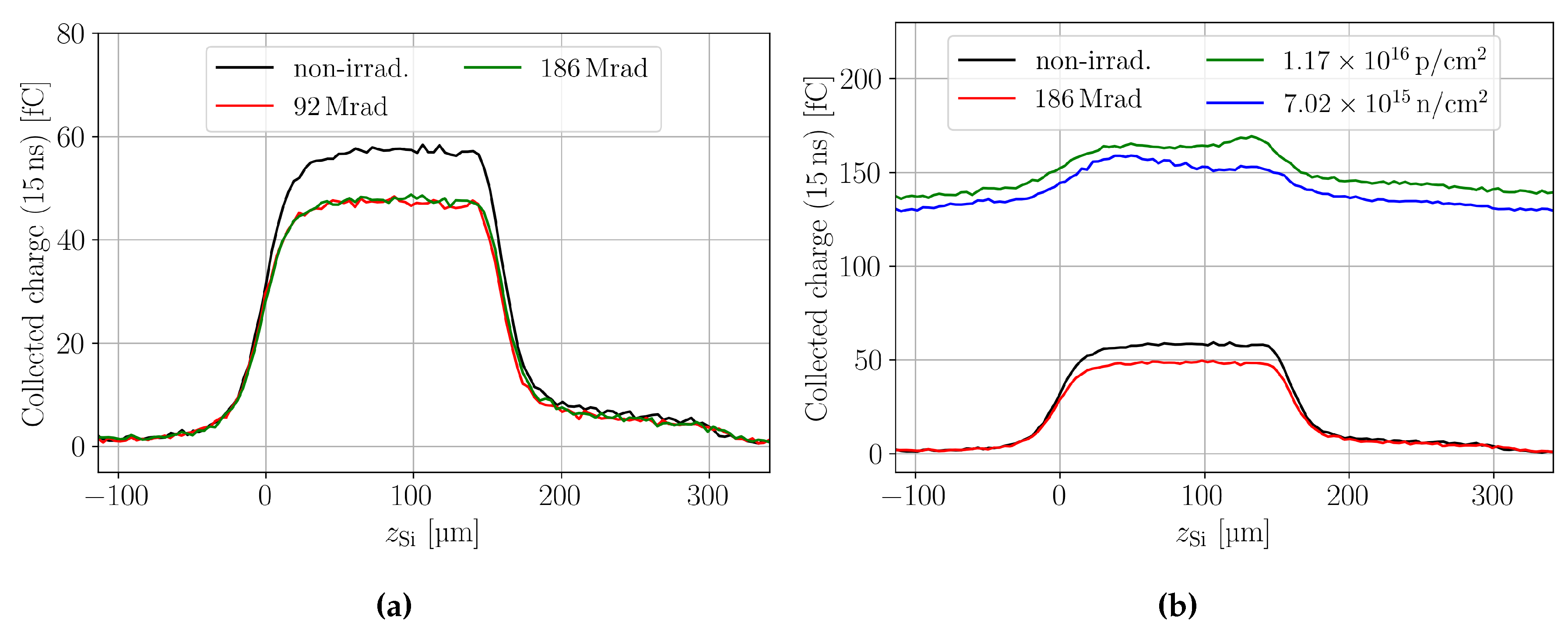
The gamma irradiation was performed with a
Co source at IRB in Zagreb [
18]. Two pad sensors irradiated to
and
are studied. In-depth CC scans are shown in
Figure 6, where a non-irradiated device is shown for comparison. It is observed that the gamma irradiation, in contrast to neutron and proton irradiation, does not introduce an SPA background. A comparison between the CC in neutron, proton, and gamma irradiated devices can be seen in
Figure 6. The gamma irradiated samples show a decrease in CC with respect to the non-irradiated device, which indicates that trapping is present. At both doses, a comparable amount of charge is collected, which is confusing as it indicates a saturation in charge loss at these doses. Such saturation is not expected from the bulk leakage current measurements of the two devices which differed by a factor of about two. Also data on gamma irradiated p-type sensors in literature do not show a saturation effect for damage parameters like leakage current and depletion voltage in the dose range studied here [
23]. Irrespective of this unresolved observation, it can be stated that the charge loss is constant throughout the two devices, contrary to the neutron and proton irradiated devices. Hence, the trapping is equal for all excess charge deposition positions, which suggests that the trapping cross-section of electrons and holes is approximately the same in the gamma irradiated samples.
3.4. Comparison of Neutron, Proton, and Gamma Irradiation
As presented above, neutron, proton, and gamma irradiation have different influences on TPA-TCT measurements. The most striking difference between hadron and gamma irradiated samples is the SPA background found in the prior, as shown in
Figure 6. In the following, it will be argued that the SPA offset is related to cluster defects. Gammas from a
Co source produce defects via Compton electrons, which do not have enough energy to create defect clusters, but only point defects [
24]. This is in contrast to hadron irradiation that creates both cluster and point defects. Concentrations of point defects introduced by neutron and gamma irradiation can be calculated using introduction rates from [
25]. The most common point defects introduced by neutron and
Co-gamma irradiation in high resistivity silicon sensors are
, and
. Neutron irradiation introduces both defects approximately proportional to the fluence. After a neutron fluence of
SPA offset is clearly visible, which corresponds to a concentration in the order of
for the
and
defects. On the other hand, gamma irradiation introduces, at the highest investigated dose, about
of these defects and thus a comparable or even higher concentration of those point defects is present. As the defect concentrations of the neutron and gamma irradiation are comparable, while the SPA offset is absent in the gamma irradiated devices, it is concluded that the SPA offset is not caused by the discussed point defects. Compared to the
and
defects, other point defects and the
defect are present in much smaller concentration and thus assumed to be less significant in the gamma irradiated devices. This gives indication that the linear light absorption found in neutron and proton irradiated devices originates from cluster and/or
defects that are not or only in very low concentration introduced by gamma irradiation. In [
20] linear absorption of
light in neutron irradiated silicon is linked to the electrically neutral divacancy V
defect state, which is introduced by neutron irradiation within cluster defects [
26]. This is in agreement with the hypothesis that the SPA background originates from cluster defects, which explains the absence of the SPA background for gamma irradiated devices.
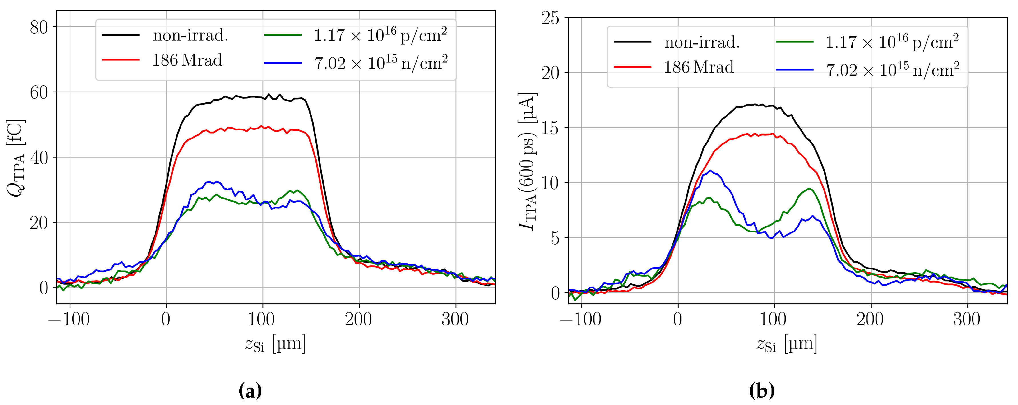
Figure 7 shows a comparison between the different irradiations for the highest fluence/dose available, where the SPA corrected CC (a) and PC (b) are shown. It can be seen that independent of the particle type, a decrease in the CC is present. Only the neutron and proton irradiated samples show variation along the device depth. Further, all particle types decrease the PC, i.e. the electric field in the device. Neutron and proton irradiation at the presented fluences leads to a double junction in the DUT, which was discussed in more detail in
Section 3.2. Both, the non-irradiated and the gamma irradiated sample show a roundish shaped PC profile, which does not agree with the expected linear behaviour in a pad detector. It is found that the roundish shape is an effect of CC during the PC time
. Smaller
or lower bias voltages decrease the roundish shape and reveal the expected linear electric field shape throughout the device depth [
12]. The effect is here especially visible as the charge is collected quickly at the used bias voltage that corresponds to about
. The PC time of
is used for a sufficient SNR that allows an easy qualitative comparison among all samples.
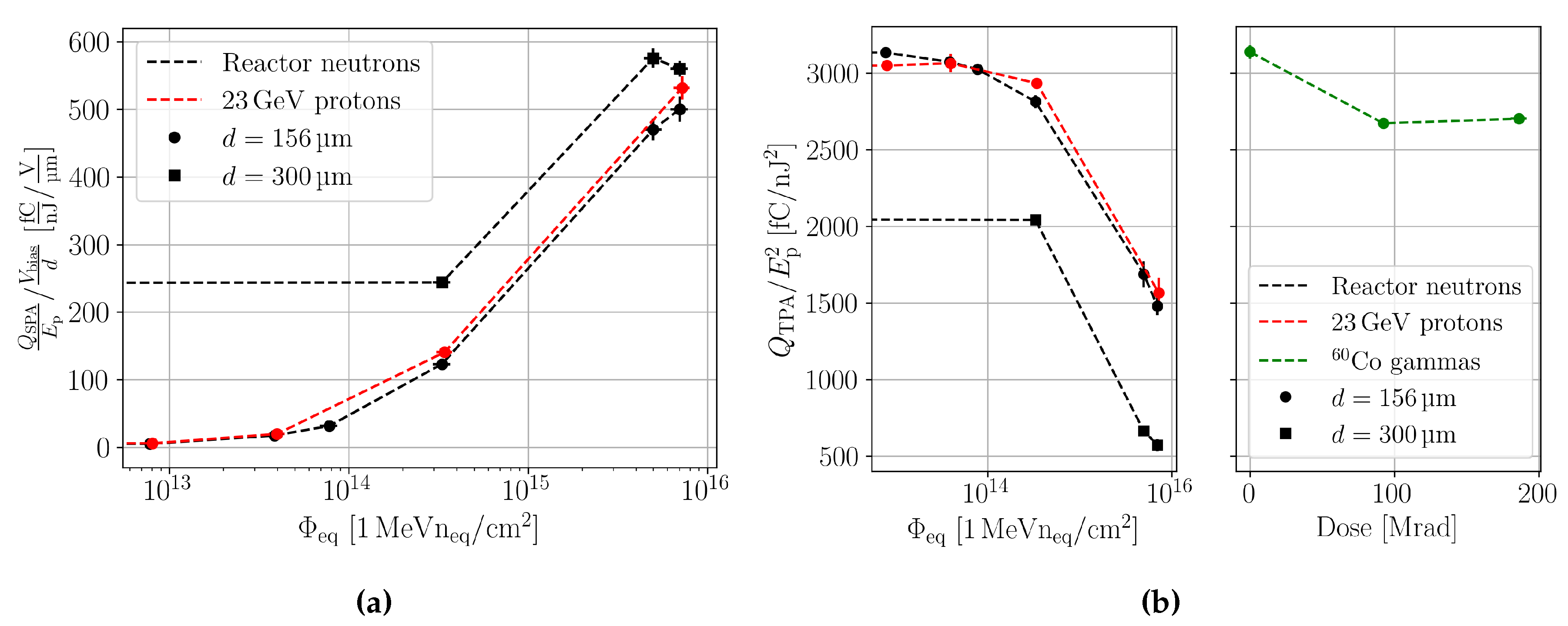
Figure 8 shows the normalised SPA (a) and TPA (b) contribution as a function of the equivalent fluence and dose. The SPA and TPA parameters are extracted from in-depth scans with the analysis procedure described in
Section 3.2. To account for the device thickness dependence of the SPA, the SPA contribution is normalised with the bias voltage over the device thickness. Thicker devices collect more SPA charge due to the higher charge generation in the increased active thickness, and they collect less TPA generated charge due to the longer drift times, as more charge carriers are trapped. It can be seen that the SPA and TPA contribution of neutron and proton irradiated samples scales similarly with the equivalent fluence, which indicates that these quantities scale with the NIEL. The scaling with the NIEL supports again the hypothesis that the SPA background origins from cluster damage.
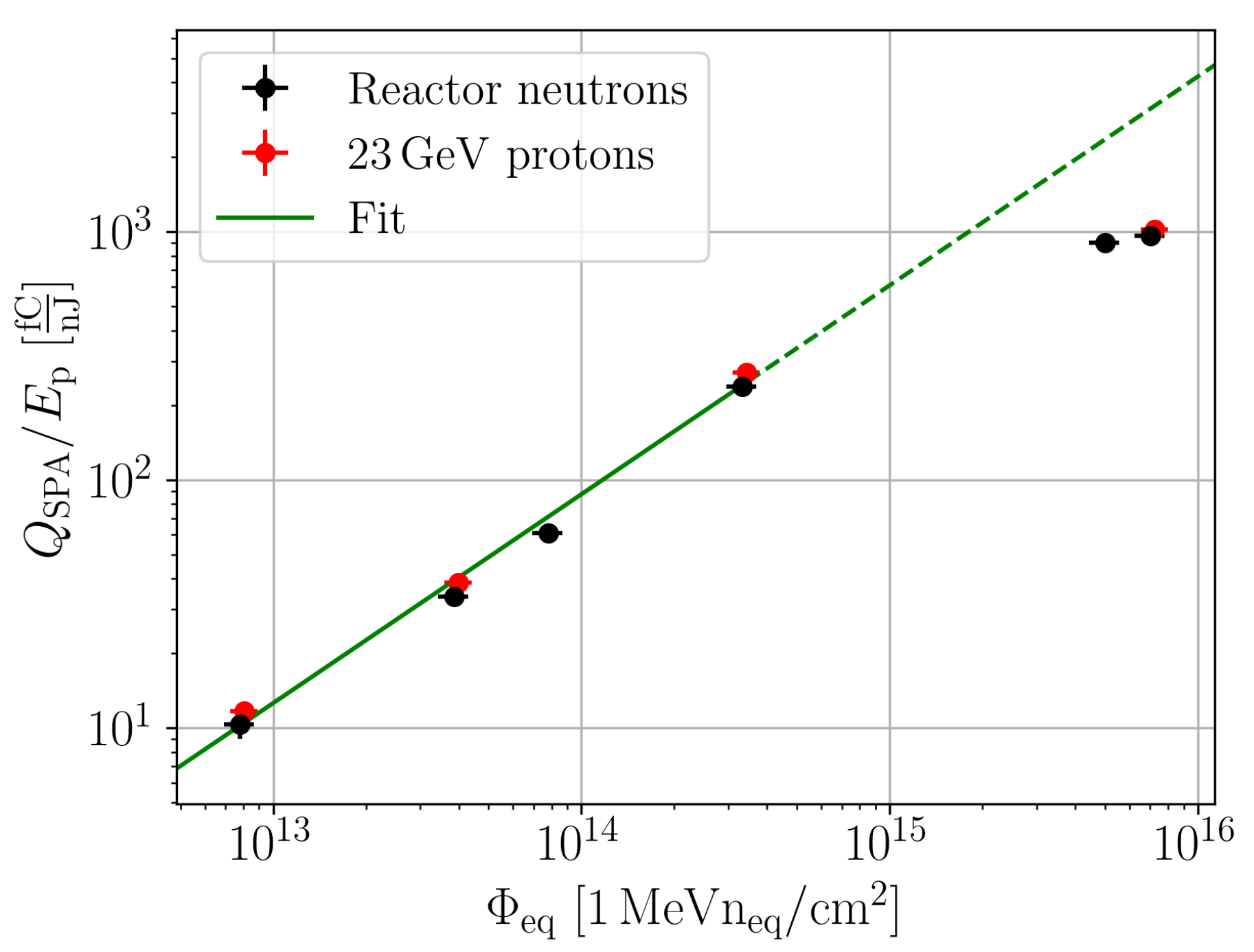
To parametrise the SPA background against the equivalent fluence, it is plotted in a log-log diagram, as shown in
Figure 9. The SPA contribution follows for fluences
a function
. Higher fluences deviate from this behaviour, and it was measured that increasing bias voltages reduced the deviations (not shown). This bias dependence indicates that the deviations are related to charge trapping that becomes apparent at the highest fluences.
3.5. Beam Depletion Due to SPA
The additional SPA contribution in irradiated devices leads to additional beam depletion, which in turn potentially leads to a decreasing TPA charge generation along the device depth. To estimate the beam depletion due to linear absorption, an effective absorption coefficient can be defined from the collected SPA charge generation:
The quotient
is obtained from the fitting of the SPA contribution (see
Figure 4 and
Figure 4). The absorption coefficient is called effective, because only absorption that generates charge that is collected is considered. Absorption that does not lead to excess charge carriers or if the excess charge carriers are trapped and not measured, they are not accounted in the effective absorption coefficient. In general the inequality
applies. Equality is reached in the absence of charge loss. When defects that absorb light but do not generated excess charge, or charge loss is present, the inequality yields:
with
being the linear absorption coefficient due to irradiation, which is defined as:
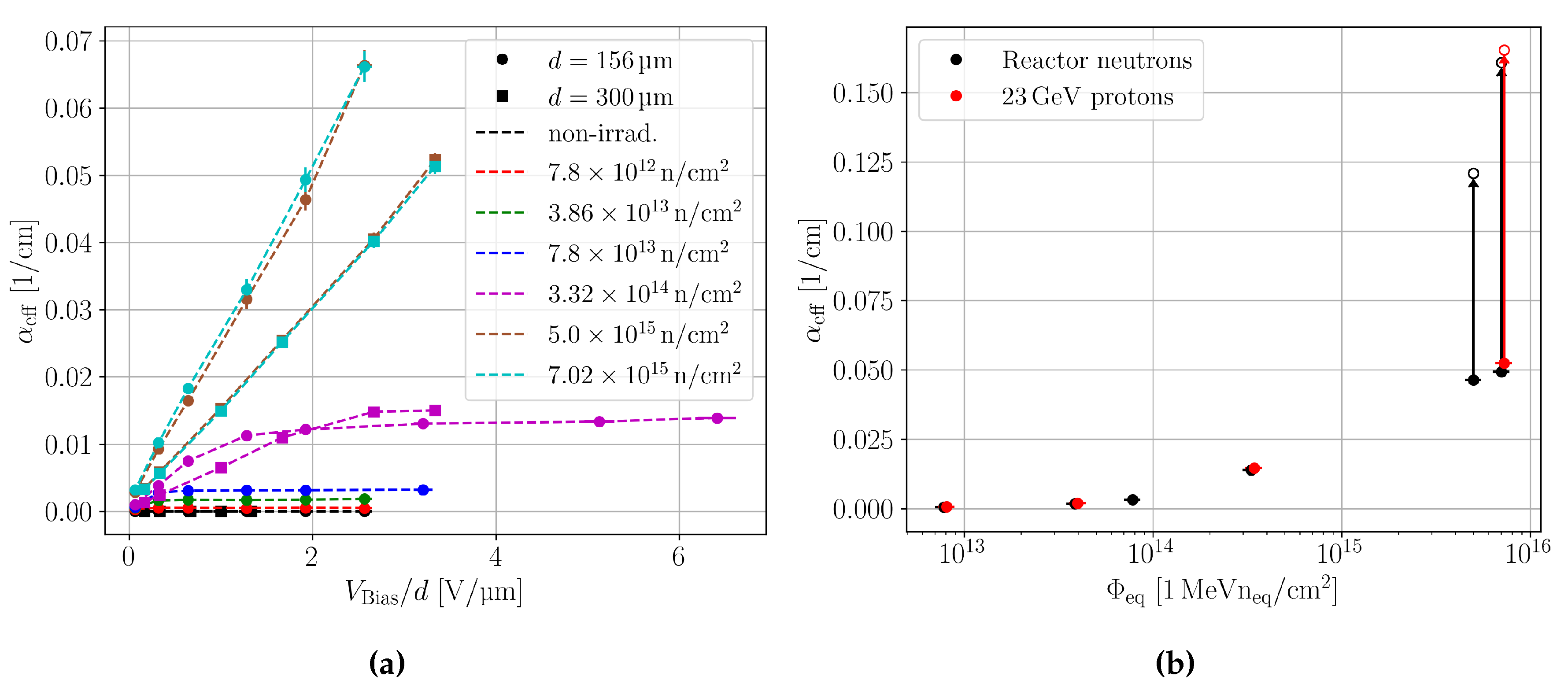
Figure 10 shows the effective linear absorption coefficient versus the bias voltage for neutron irradiated pad sensors with different thicknesses.
increases with the bias voltage and saturates within the investigated voltage range for fluences up to
. The maximum absorption coefficient for these fluences is below
, which leads to a beam depletion below
in a
thick silicon detector. Such low intensity loss can be neglected. Thicker devices yield lower
, because the charge loss is more pronounced, which increases the inequality of equation (
2). Higher fluences do not reach saturation within the used bias voltage range, because the charge loss does not saturate up to the maximum bias voltage.
Figure 10 shows the effective absorption coefficient for neutron and proton irradiated pad detectors versus the equivalent fluence. As the SPA charge collection does not saturate for the highest fluences, only a lower limit for
is stated. From the measured data it is ensured that the beam is not depleted by the SPA absorption for fluences up to at least
. The effective absorption coefficient does not saturate for higher fluences, which hinders to investigate the absolute beam depletion. Reference [
20] measures
for a fluence of
in non-biased detector grade silicon, which corresponds to less than
absorption in a
thick device. In conclusion, beam depletion in irradiated devices due to SPA for fluences up to at least
is assumed to be negligible.
3.6. Influence on the Two Photon Absorption Coefficient
In the above presented measurements it is observed that irradiation decreases the charge collection. However, the reliability of the collected data is not ensured, because the charge generation mechanism of TPA might be impacted by the irradiation, meaning that the absorption coefficient might be a function of fluence. To investigate the fluence dependence of , a comparative CC study was performed using a Sr setup. Charge sensitive amplifiers are used to increase the SNR. The thick, neutron irradiated subset is used for this study and the non-irradiated detector from the same wafer serves as a reference.
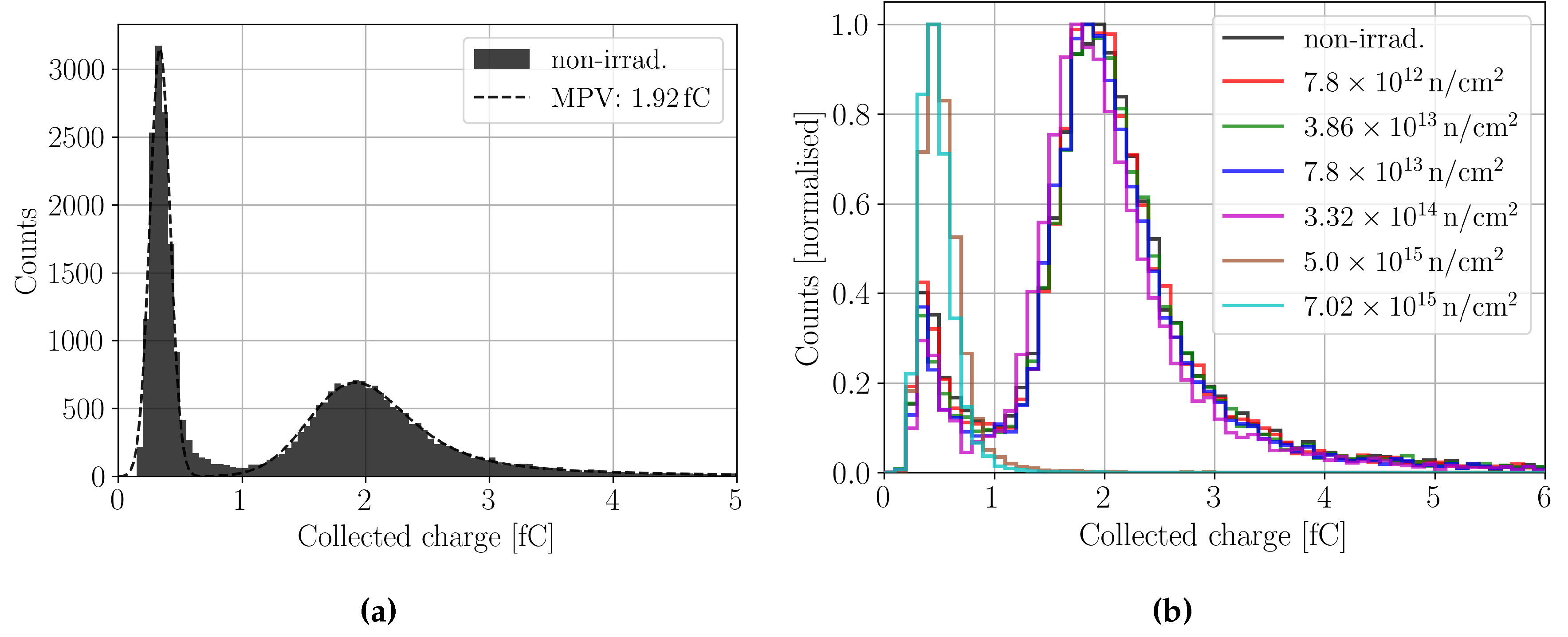
An example for the CC measurement in a non-irradiated device in shown in
Figure 11. It can be seen that the CC resembles the expected Landau-Gauss distribution and an additional noise peak for charge
is measured. The main part of the CC distribution is fitted with a Landau-Gauss distribution and the noise peak is fitted by a Gaussian distribution [
27]. The used fitting functions yield a satisfactory agreement with the data and allow to extract the most probable value (MPV) from the distribution, which corresponds to the generated charge of a minimum ionising particle (MIP). The MPV (
) needs to be corrected with the mean of the noise floor (
) to obtain the MIP charge. For a non-irradiated detector the MPV is found as
electron-hole pairs, which is in good agreement with expectations from literature [
28].
Figure 11 shows the evolution of the CC with increasing neutron irradiation. To suppress noise as efficient as possible, the distributions are filtered by the following criteria: the peaking time of the DUT needs to agree within a time frame of
around the peaking time of the reference. When the CC of the non-irradiated device in
Figure 11 is compared to
Figure 11 it is evident that the used criteria suppresses noise efficiently. Even after the applied criteria some noise remains, because the noise is randomly distributed in time. It is observed that the CC decreases with fluence due to the increasing charge trapping. At a certain fluence, the signal and noise distribution begin to overlap, which hinders the extraction of the MPV. Here, for fluences
the extraction of the MPV is no longer possible.
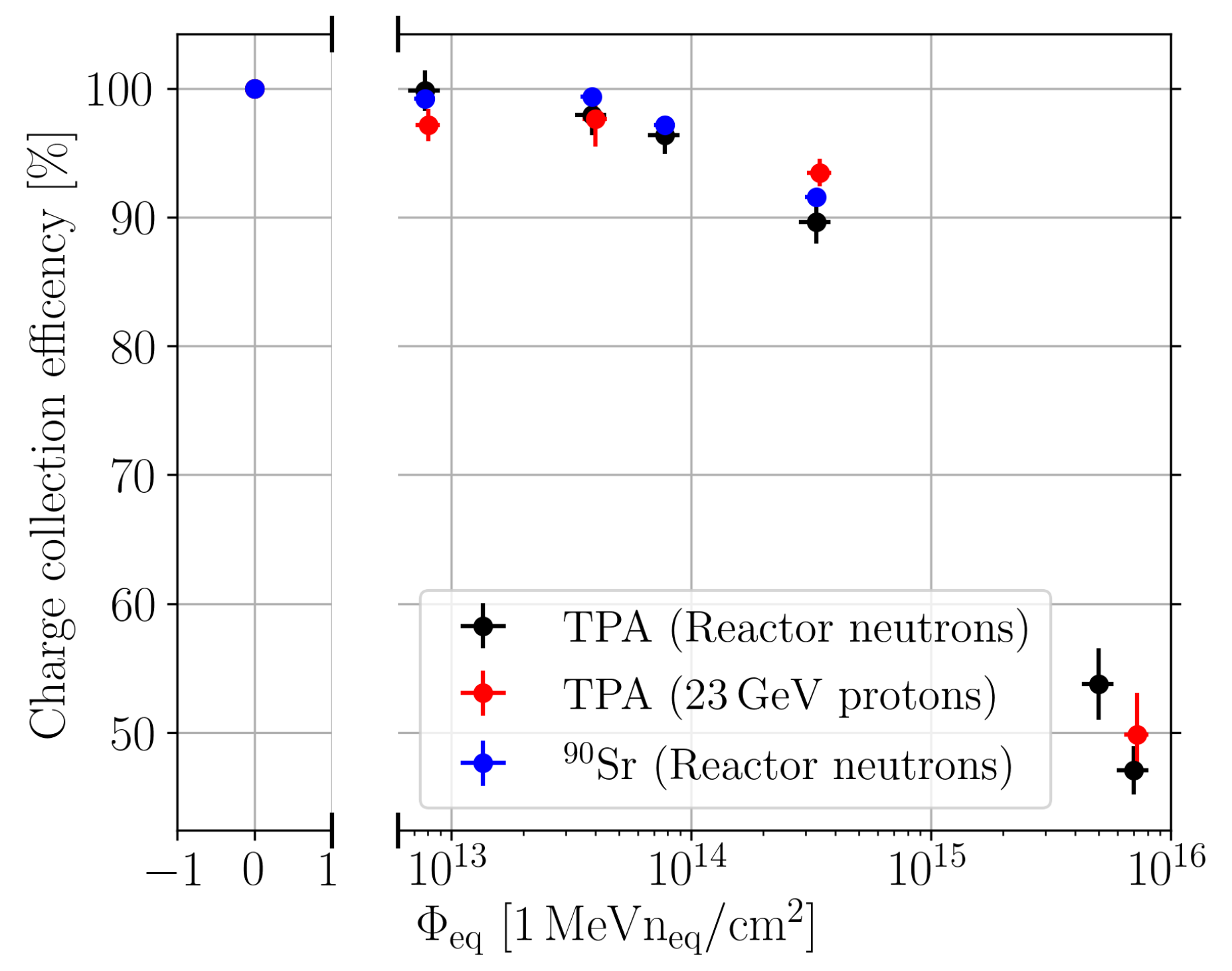
Figure 12 shows charge collection efficiency (CCE) against the equivalent fluence measured with the TPA-TCT setup and the
Sr setup. The CCE is defined as the percentage of charge that is collected in comparison to the non-irradiated device. For the
Sr setup this means the normalisation of the MPV with the MPV of the non-irradiated device and for the TPA-TCT the fitting parameters for
described in
Section 3.2 is normalised with the fitting parameters from the non-irradiated device. The data from the proton irradiated devices is included even though they were only measured with the TPA-TCT. It can be seen that both techniques yield, within the measurement uncertainty, a compatible CCE. The compatibility of both techniques indicates that the charge generation mechanism of TPA and the
particle of the
Sr source scales similar with fluence up to at least
. As the excess charge generation by the two process is very different from the ionisation process of a
particle, the similarity of the CCE measurements strongly hints that the charge generation mechanism of TPA, i.e. the absorption coefficient
, is constant with irradiation
up to a fluence of at least
. Contrary to
, the SPA coefficient
is fluence dependent (see
Section 3.1 and [
20]).
Besides the investigation of , it can be seen that the TPA-TCT provides CCEs values even for fluences that are not accessible with the used Sr setup. This has two reasons: first, the intensity of the laser can be increased to much more than one MIP equivalent of charge and second, averages for multiple acquisitions are available, as the charge generation of the laser is reproducible pulse-per-pulse. Both reasons significantly increase the SNR. In contrast, the Sr setup relies on single acquisition, because the charge generation is a stochastic process and the events are uncorrelated. Further, the setup triggers on the coincidence of the two reference detectors and in order to mitigate influences on the DUT’s signal acquisition, the DUT is not included in the trigger. Hence, it is not ensured that the DUT records a particle hit for every acquisition, which leads to the noise floor. In conclusion, it was demonstrated that the TPA-TCT allows performing CCE measurements similar to a Sr setup. The TPA-TCT offers an extended measurement range. Moreover, the TPA-TCT allows to study the CCE against the device depth, which was not shown here, because the aim of these measurements was to investigate the effects of radiation damage on , wherefore a study of a depth dependent CCE is not presented and the mean over the full device depth was used.
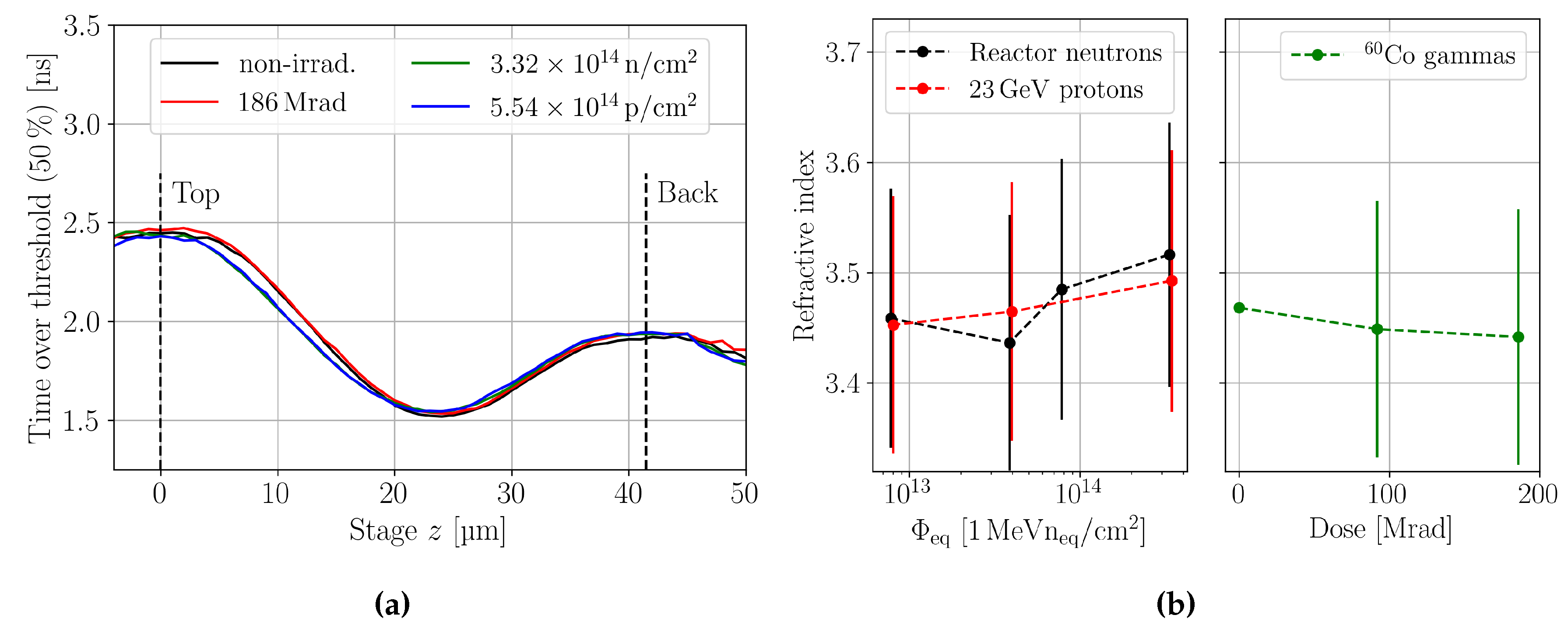
3.7. Refractive Index
Irradiation potentially changes the refractive index of silicon, as was observed for the bombardment with heavy ions [
29]. A changing refractive index influences the reflectance of the material and thus the amount of generated charge. In this section, the refractive index is studied indirectly from TPA-TCT in-depth scans by exploitation of the refraction at the top air-silicon interface. Refraction is described by [
8]:
with the refractive index
n, the Rayleigh length
, and the wavelength
. The equation can be rearranged to the squared refractive index
with
and
. Therefore, a study of the scaling allows drawing conclusions on the refractive index. If irradiation changes the refractive index, the scaling factor would depend on the fluence and dose, so that the boundary interfaces of the devices would appear at different positions in the uncorrected coordinate system. As all devices are from the same wafer, the assumption of the same thicknesses is reasonable. The position of the boundaries is extracted from in-depth scan. The back side surface is found from symmetries in the ToT profile, wherefore such plots are well suited to qualitatively compare the devices thicknesses.
Figure 13 shows ToT profiles in uncorrected
z-coordinates, where the positions on the top and back side surface extracted from the non-irradiated device are indicated. It is visualised that all devices, independent of their irradiation, have the interfaces at about the same position, which indicates that the refractive index is expected to be reasonably independent of irradiation. Aside the boundary positions, the hadron irradiated devices show differences in the ToT at the top side and only slight differences at the back side. The difference at the top side is related to hole trapping, which is more severe than the electron trapping, thus a less significant difference is present at the back side.
A quantitative study of the refractive index is performed using the scaling factor, which is found by comparing the extracted device thicknesses in stage coordinates, i.e. uncorrected coordinates. The boundaries are extracted from fits towards the SPA corrected charge profile of all devices individually. The scaling factor is found by comparison with the non-irradiated device and the refractive index is then calculated from equation (
5) This procedure is performed for all devices that do not show the double junction effect, because the double junction is found to dominate the ToT profile, which hinders the extraction of the device’s boundaries. The results are summarised in
Figure 13. No trend with the equivalent fluence is observed, and all measured values are compatible with the nominal value of the non-irradiated device. The error bars are quite large, because the used method is only indirect, and many measurement uncertainties propagate to yield the presented errors. In conclusion, it is found that if irradiation changes the refractive index, the change due to equivalent fluences up to
and doses up to
is
to its nominal value. Therefore, a fluence independent refractive index is a reasonable assumption for the investigated fluence range.
4. Conclusions
Neutron, proton, and gamma irradiated pad detectors were systematically studied using the TPA-TCT. A main finding was the absence of a single photon absorption (SPA) background for gamma irradiated devices, contrary to irradiation with neutron or proton. For the latter it was found that the SPA background scales with the equivalent fluence, which indicates that it is related to bulk damage and in accordance with the non-ionising energy loss (NIEL) hypothesis. The functional relation for the SPA induced charge was measured to be for thick sensors. Absence of the SPA background in gamma irradiated devices and the scaling of the SPA background with NIEL indicate that the occurrence of SPA is related to cluster damage. Differences in the prompt current profile between neutron and proton irradiated devices were observed for . Both devices showed a double junction, and the proton irradiated device appeared type-inverted compared to the neutron irradiated device, meaning that the electric field starts to grow from the back electrode with rising voltage. This proton irradiation related inversion could be relevant to p-type strip detectors as it potentially leads to a decreased charge collection efficiency (CCE) compared to similar neutron irradiated strip detectors.
It was measured that the additional SPA contribution does not lead to a meaningful beam depletion in silicon devices up to fluences of at least , which is important in order to obtain comparable charge generation along the device depth of irradiated devices. Further, it was verified that the refractive index and the absorption coefficient agree with their nominal values for fluences up to at least . In general, it was demonstrated that the TPA-TCT produces meaningful results for irradiated devices and is a valuable addition to the present set of available characterisation methods.
Author Contributions
Conceptualization, M.M. and S.P.; methodology, M.F.G., S.P., and M.W.; software, M.F.G. and S.P.; validation, S.P.; formal analysis, S.P.; investigation, S.P.; resources, M.M.; data curation, S.P.; writing—original draft preparation, S.P.; writing—review and editing, M.F.G., M.M. and M.W.; visualization, S.P.; supervision, M.M.; project administration, M.M.; funding acquisition, M.M. All authors have read and agreed to the published version of the manuscript.
Funding
This project was performed within the framework of RD50 and DRD3 and has received funding from the European Union’s Horizon 2020 Research and Innovation programme under GA no 101004761 (AIDAinnova), the Wolfgang Gentner Program of the German Federal Ministry of Education and Research (grant no. 05E18CHA), and the CERN Knowledge Transfer Fund, through a grant awarded in 2017.
Informed Consent Statement
Not applicable.
Data Availability Statement
The data presented in this study are available on request from the corresponding author. The data are not publicly available due to the complexity of the data and to maintain an overview on usage.
Acknowledgments
Not applicable.
Conflicts of Interest
The authors declare no conflict of interest. The funders had no role in the design of the study; in the collection, analyses, or interpretation of data; in the writing of the manuscript; or in the decision to publish the results.
Abbreviations
The following abbreviations are used in this manuscript:
| CC |
Collected charge |
| CCE |
Charge collection efficiency |
| DUT |
Device under test |
| FWHM |
Full width at half maximum |
| MIP |
Minimum ionising particle |
| MPV |
Most probable value |
| PCB |
Printed circuit board |
| SNR |
Signal-to-noise ratio |
| SPA |
Single Photon Absorption |
| TCT |
Transient Current Technique |
| ToT |
Time over threshold |
| TPA |
Two Photon Absorption |
References
- Eremin, V.; Strokan, N.; Verbitskaya, E.; Li, Z. Development of transient current and charge techniques for the measurement of effective net concentration of ionized charges (Neff) in the space charge region of p-n junction detectors. Nuclear Instruments and Methods in Physics Research A: Accelerators, Spectrometers, Detectors and Associated Equipment 1996, 372, 388–398. [Google Scholar] [CrossRef]
- Mandić, I.; Cindro, V.; Gorišek, A.; Kramberger, G.; Mikuž, M.; Zavrtanik, M. Observation of full charge collection efficiency in heavily irradiated n+p strip detectors irradiated up to 3×10¹⁵neq/cm2. Nuclear Instruments and Methods in Physics Research A: Accelerators, Spectrometers, Detectors and Associated Equipment 2010, 612, 474–477. [Google Scholar] [CrossRef]
- Casse, G.; Allport, P.; Booth, P.; Greenall, A.; Jackson, J.; Jones, T.; Smith, N.; Turner, P.; Carter, J.; Morgan, D.; Robinson, D.; Beck, G.; Carter, A. A comparative study of oxygenated and non-oxygenated Si pad diodes, miniature and large area microstrip detectors. Nucl. Instrum. Methods Phys. Res. A: Accel., Spectrom., Detect. Assoc. Equip. 2001, 466, 335–344. [Google Scholar] [CrossRef]
- Wiehe, M.; Fernández García, M.; Moll, M.; Montero, R.; Palomo, F.R.; Vila, I.; Muñoz-Marco, H.; Otgon, V.; Pérez-Millán, P. Development of a Tabletop Setup for the Transient Current Technique Using Two-Photon Absorption in Silicon Particle Detectors. IEEE Transactions on Nuclear Science 2021, 68, 220–228. [Google Scholar] [CrossRef]
- Fernández García, M.; Jaramillo Echeverría, R.; Moll, M.; Montero, R.; Palomo Pinto, R.; Vila, I.; Wiehe, M. High resolution 3D characterization of silicon detectors using a Two Photon Absorption Transient Current Technique. Nuclear Instruments and Methods in Physics Research Section A: Accelerators, Spectrometers, Detectors and Associated Equipment 2020, 958, 162865. [Google Scholar] [CrossRef]
- Vila Álvarez, I.; De Castro Manzano, P.; Fernández García, M.; González, J.; Jaramillo Echevarría, R.; Moll, M.; Montero, R.; Palomo Pinto, F.R. TPA-TCT: A novel Transient Current Technique based on the Two Photon Absorption (TPA) process. 25th RD50 Workshop (CERN), 2014.
- Palomo Pinto, F.R.; Vila Álvarez, I.; De Castro Manzano, P.; Fernández García, M.; Moll, M. Two Photon Absorption and carrier generation in semiconductors. 25th RD50 Workshop (CERN), 2014.
- Wiehe, M. Development of a Two-Photon Absorption - TCT system and Study of Radiation Damage in Silicon Detectors. PhD thesis, Albert-Ludwigs-Universität Freiburg im Breisgau, 2021.
- Pape, S.; Currás, E.; Fernández García, M.; Moll, M. Techniques for the Investigation of Segmented Sensors Using the Two Photon Absorption-Transient Current Technique. Sensors 2023, 23. [Google Scholar] [CrossRef] [PubMed]
- Fernández García, M.; González Sánchez, J.; Jaramillo Echeverría, R.; Moll, M.; Montero, R.; Moya, D.; Palomo Pinto, F.R.; Vila, I. On the determination of the substrate effective doping concentration of irradiated HV-CMOS sensors using an edge-TCT technique based on the Two-Photon-Absorption process. JINST 2017, 12, C01038. [Google Scholar] [CrossRef]
- Pape, S.; Fernández García, M.; Moll, M.; Montero, R.; Palomo, F.; Vila, I.; Wiehe, M. Characterisation of irradiated and non-irradiated silicon sensors with a table-top two photon absorption TCT system. Journal of Instrumentation 2022, 17, C08011. [Google Scholar] [CrossRef]
- Pape, S. Characterisation of Silicon Detectors Using the Two Photon Absorption – Transient Current Technique. PhD thesis, TU Dortmund University, 2024.
- Almagro-Ruiz, A.; Pape, S.; Muñoz-Marco, H.; Wiehe, M.; Currás, E.; Fernández-García, M.; Moll, M.; Montero, R.; Palomo, F.R.; Quintana, C.; Vila, I.; Pérez-Millán, P. Fiber laser system of 1550nm femtosecond pulses with configurable properties for the two-photon excitation of transient currents in semiconductor detectors. Appl. Opt. 2022, 61, 9386–9397. [Google Scholar] [CrossRef] [PubMed]
- CIVIDEC Instrumentation GmbH, Vienna, Austria. https://cividec.at/index.php, accessed on 2023-09-26.
- CiS Forschungsinstitut für Mikrosensorik GmbH, Erfurt, Germany. https://www.cismst.de/, accessed on 2023-09-26.
- Jožef Stefan Institute, Ljubljana, Slovenia. https://www.ijs.si/ijsw/JSI, accessed on 2024-02-15.
- PS-IRRAD Proton Facility, CERN, Switzerland. https://ps-irrad.web.cern.ch/ps-irrad, accessed on 2024-02-15.
- Ruđer Bošković Institute, Zagreb, Croatia. https://www.irb.hr/eng, accessed on 2024-02-15.
- Snoj, L.; Žerovnik, G.; Trkov, A. Computational analysis of irradiation facilities at the JSI TRIGA reactor. Applied Radiation and Isotopes 2012, 70, 483–488. [Google Scholar] [CrossRef] [PubMed]
- Fretwurst, E.; Klanner, R.; Schwandt, J.; Vauth, A. Study of the V20 state in neutron-irradiated silicon using photon-absorption measurements. Nuclear Instruments and Methods in Physics Research A: Accelerators, Spectrometers, Detectors and Associated Equipment 2023, 1053, 168353. [Google Scholar] [CrossRef]
- Eremin, V.; Verbitskaya, E.; Li, Z. The origin of double peak electric field distribution in heavily irradiated silicon detectors. Nucl. Instrum. Methods Phys. Res. A: Accel., Spectrom., Detect. Assoc. Equip. 2002, 476, 556–564. [Google Scholar] [CrossRef]
- Spieler, H. Semiconductor Detector Systems, 1 ed.; Oxford University press, 2005.
- Zatocilova, I.; Mikestikova, M.; Latonova, V.; Kroll, J.; Privara, R.; Novotny, P.; Dudas, D.; Kvasnicka, J. Study of bulk damage of high dose gamma irradiated p-type silicon diodes with various resistivities. Journal of Instrumentation 2024, 19, C02039. [Google Scholar] [CrossRef]
- Moll, M. Displacement Damage in Silicon Detectors for High Energy Physics. IEEE Transactions on Nuclear Science 2018, 65, 1561–1582. [Google Scholar] [CrossRef]
- Moll, M. Radiation damage in silicon particle detectors. Microscopic defects and macroscopic properties. PhD thesis, University of Hamburg, 1999. [CrossRef]
- van Lint, V.A.J.; Leadon, R.E.; Colwell, J.F. Energy Dependence of Displacement Effects in Semiconductors. IEEE Transactions on Nuclear Science 1972, 19, 181–185. [Google Scholar] [CrossRef]
- Davidek, T.; Leitner, R. Parametrization of the Muon Response in the Tile Calorimeter. Technical report, CERN-ATL-TILECAL-97-114, 1997.
- Hartmann, F. Evolution of Silicon Sensor Technology in Particle Physics, 2 ed.; Springer Nature, 2017. [CrossRef]
- Heidemann, K.F. Complex-refractive-index profiles of 4 MeV Ge ion-irradiation damage in silicon. Philosophical Magazine B 1981, 44, 465–485. [Google Scholar] [CrossRef]
- Li, H.H. Refractive index of silicon and germanium and its wavelength and temperature derivatives. Journal of Physical and Chemical Reference Data 1980, 9, 561–658. [Google Scholar] [CrossRef]
Figure 1.
Sketch of the used table top TPA-TCT setup.
Figure 1.
Sketch of the used table top TPA-TCT setup.
Figure 2.
(a) Charge versus depth profile of an irradiated () thick p-type planar pad detector. The bias voltage is . A comparison of the three different SPA correction methods is shown. The waveform subtraction method is indicated by the index WF, the subtraction method by the index const, and the correction by intensity method by the index I. The uncorrected data are given without index. (b) Time over threshold measurement in the same pad detector, including a comparison of the waveform subtraction and the intensity correction method.
Figure 3.
In-depth scans of the charge collection in pad detectors for neutron (a) and proton (b) irradiated samples. Figure (c) and (d) show the SPA corrected in-depth scans for neutrons and protons, respectively. The bias voltage is .
Figure 3.
In-depth scans of the charge collection in pad detectors for neutron (a) and proton (b) irradiated samples. Figure (c) and (d) show the SPA corrected in-depth scans for neutrons and protons, respectively. The bias voltage is .
Figure 4.
Charge collected by SPA in neutron (a) and proton (b) irradiated thick pad sensors. Charge collected by TPA for the same neutron (c) and proton (d) irradiated devices. The TPA charge is extracted as the mean of the collected charge between the FWHM of the in-depth scans. The bias voltage for all scans is .
Figure 5.
Prompt current at for different bias voltages measured for (a) a neutron fluence of and (b) a proton fluence of . The equivalent fluences are comparable. The double junction is clearly visible in both plots. The proton irradiated sample shows an electric field that grows from, and is stronger at, the back electrode. This effect is often called type inversion.
Figure 6.
(a) In-depth scans of the charge collection in pad detectors. Gamma irradiated samples and a non-irradiated sample are shown. (b) Comparison between the in-depth scans of a non-irradiated, a neutron, a proton, and a gamma irradiated pad sensor. The bias voltage in all scans is .
Figure 6.
(a) In-depth scans of the charge collection in pad detectors. Gamma irradiated samples and a non-irradiated sample are shown. (b) Comparison between the in-depth scans of a non-irradiated, a neutron, a proton, and a gamma irradiated pad sensor. The bias voltage in all scans is .
Figure 7.
(a) In-depth scans of the charge collection in pad detectors. A non-irradiated sample is shown as well as a neutron, a proton, and a gamma irradiated sample. (b) Same in-depth scans, but the SPA offset is corrected by the waveform subtraction method. The bias voltage is .
Figure 7.
(a) In-depth scans of the charge collection in pad detectors. A non-irradiated sample is shown as well as a neutron, a proton, and a gamma irradiated sample. (b) Same in-depth scans, but the SPA offset is corrected by the waveform subtraction method. The bias voltage is .
Figure 8.
(a) SPA charge collection normalised with the average electric field versus the equivalent fluence for neutron and proton irradiated FZ p-type pad detector. (b) TPA charge collection versus the equivalent fluence and dose for the same DUT.
Figure 8.
(a) SPA charge collection normalised with the average electric field versus the equivalent fluence for neutron and proton irradiated FZ p-type pad detector. (b) TPA charge collection versus the equivalent fluence and dose for the same DUT.
Figure 9.
Charge collected by SPA normalised with the pulse energy for proton and neutron irradiated in thick pad detectors, biased to . The fit function is of the form , with and . The highest fluences are excluded from the fit.
Figure 9.
Charge collected by SPA normalised with the pulse energy for proton and neutron irradiated in thick pad detectors, biased to . The fit function is of the form , with and . The highest fluences are excluded from the fit.
Figure 10.
(a) Effective linear absorption coefficient of neutron irradiated pad detectors versus the bias voltage, which is normalised with the device thickness. (b) Effective linear absorption coefficient for
thick neutron and proton irradiated pad detectors versus the equivalent fluence. The value for the maximum bias voltage is used. The absorption coefficient does not saturate for the highest fluences and the highest applied bias voltage is different for the proton and neutron irradiated devices. In order to show comparable
for the highest fluences, a bias voltage of
is selected. The arrows are used to guide the eye towards the empty markers. These show the
calculated from the interpolated
of
Figure 9.
Figure 11.
(a) Charge collection of a non-irradiated thick p-type pad sensor measured in a Sr setup. (b) Charge collection in neutron irradiated pad sensors for different fluences. The histogram is normalised to the maximum amount of counts to ease the comparison. The bias voltage in all measurements is .
Figure 12.
Charge collection efficiency for pad sensors, measured with the TPA-TCT and a Sr setup, against the equivalent fluence. The type of irradiation is mentioned in the legend.
Figure 12.
Charge collection efficiency for pad sensors, measured with the TPA-TCT and a Sr setup, against the equivalent fluence. The type of irradiation is mentioned in the legend.
Figure 13.
(a) Time over threshold profiles of the non-irradiated and the irradiated pad detectors. The highest fluences, while avoiding the double junction effect, are used to allow the comparison. The refraction from the air-silicon interface is not corrected in the
z-axis. The location of the top and back interface is extracted from the non-irradiated device, and they are indicated by the dashed lines. (b) Refractive index extracted from the in-depth scans of various irradiated pad detectors. The nominal refractive index
is taken from [
30]. All scans are performed with a bias voltage of
.
Table 1.
Details of the used pad sensors. All devices are fabricated by CiS in the CiS16 campaign and have a FZ p-type bulk with a pre-irradiation resistivity .The proton fluences are given in absolute values, while the neutron fluences represent the neutron equivalent fluences.
Table 1.
Details of the used pad sensors. All devices are fabricated by CiS in the CiS16 campaign and have a FZ p-type bulk with a pre-irradiation resistivity .The proton fluences are given in absolute values, while the neutron fluences represent the neutron equivalent fluences.
| Name |
Active |
Fluence/ |
Annealing |
| |
thickness []
|
Dose |
|
| Pristine |
| 21-DS-79 |
|
– |
– |
| 25-DS-66 |
|
|
|
| Neutron [] |
| 21-DS-78 |
|
|
at
and
at
|
| 21-DS-84 |
|
|
|
| 21-DS-98 |
|
|
|
| 21-DS-99 |
|
|
|
| 21-DS-101 |
|
|
|
| 21-DS-102 |
|
|
|
| 25-DS-104 |
|
|
|
| 25-DS-87 |
|
|
|
| 25-DS-88 |
|
|
|
| Proton [] |
| 21-DS-97 |
|
|
at
and
at
|
| 21-DS-96 |
|
|
|
| 21-DS-94 |
|
|
|
| 21-DS-92 |
|
|
|
| Gamma [] |
| 19-DS-97 |
|
|
- |
| 19-DS-99 |
|
|
|
|
Disclaimer/Publisher’s Note: The statements, opinions and data contained in all publications are solely those of the individual author(s) and contributor(s) and not of MDPI and/or the editor(s). MDPI and/or the editor(s) disclaim responsibility for any injury to people or property resulting from any ideas, methods, instructions or products referred to in the content. |
© 2024 by the authors. Licensee MDPI, Basel, Switzerland. This article is an open access article distributed under the terms and conditions of the Creative Commons Attribution (CC BY) license (http://creativecommons.org/licenses/by/4.0/).
