1. Introduction
Recent advances in new wireless communication platforms (satellite communications, 5G and 6G wireless communications) promise improved coverage, higher capacity, higher data rates, more efficient use of spectrum resources, lower latency, greater system reliability, and increased flexibility, [
1,
2]. The evolution of wireless networks is also driven by the deployment of fiber optic networks due to an increasing number of subscribers. Future 6G mobile communications networks are expected to achieve higher communication capacities, which would require a substantial increase in bandwidth, [
3,
4].
As higher frequencies are used to transmit information, wireless communications will experience higher propagation losses and blockage effects from obstacles. To address this, electronically steerable antennas will be required, which can be achieved using functional material technology such as liquid crystal (LC), [
5].
Since high-frequency communications (millimeter waves and future THz communications) necessitate smaller devices, it has been observed that at high frequencies, microstrip technology suffers from surface waves and high losses, degrading performance. Waveguide technology is also not a cost-effective solution and poses challenges in integration with networks and antennas, [
6].
Thus, Groove Gap Waveguide (GGW) technology and its variations, Ridge Groove Gap Waveguide (RGW) and Microstrip Ridge Groove Gap Waveguide (MRGW), have emerged. These technologies offer advantages over the previously mentioned ones: no need for good mechanical contact between the cover and the body enclosing a waveguide cavity, lower insertion losses, and suppression of surface standing waves. This technology utilizes an artificial magnetic wall (PMC), characterized by high surface impedance, creating a EM bandgap where only fundamental EM field propagates, [
7].
In this work, MRGW technology has been chosen because it allows the integration of functional materials like LC with planar technologies based on microstrip. Consequently, due to the needs of current wireless and satellite communications, as well as future 6G communications, a series of compact MRGW-LC devices will be developed: the phase shifter and the stub resonator.
For proper analysis, the electromagnetic simulation software CST Studio Suite, v. 2024, will be used. Simulations will be performed using the finite element method to solve the electromagnetic problem of the circuits, and the eigenvalue problem-solving method will be used to analyze the perfect magnetic conductor (PMC) formed by high impedance surface (HIS) to extract single-mode EM bandgap (as well known as EM stopband).
2. Materials and Methods
This section will examine the methodology for the parameter extraction and the topology of the microwave MRGW-LC circuits and the coating of an alignment layer valid on the copper cladding of commercially printed board circuits (PCBs), the assembling and filling of the whole structure, and finally the measurement setup.
2.1. Fundamentals of Liquid Crystal
Liquid crystals are anisotropic materials that exhibit intermediate phases (mesophases) between solid/crystalline and fluid/isotropic states. In RF applications, LCs consist of elongated rod-like molecules (calamitic LCs) that typically display a nematic phase at room temperature. In this phase, the molecules flow as liquids but maintain long-range directional (orientational) order, [
8].
The use of nematic liquid crystals (LCs) has the disadvantage that many have not been characterized at microwave frequencies (300 MHz – 300 GHz), which include millimeter waves, making it difficult to predict their behavior at these frequencies. However, nematic LCs have been used not only in optical devices but also at microwave frequencies. LCs are of interest for use in reconfigurable devices at microwave frequencies because they exhibit lower losses at higher frequencies. For example, a significant number of scientific articles have reported on steerable antennas [
9], phase shifters [
10,
11], and filters [
12,
13].
Macroscopically, the anisotropic structure of nematic liquid crystals (LCs) can be described by a director vector (
n) representing the average direction of the long axis of the LC molecules. The dielectric permittivity of this material is defined by the angle between this director and the applied electric field. Consequently, nematic LCs have two principal permittivities: parallel to the director vector (
) and perpendicular to the director vector (
). LCs are polar and exhibit an electric dipole moment, allowing the reorientation of molecules using a continuous or low-frequency electric field (around 1 kHz) or a magnetic field. This results in a uniaxial anisotropic material whose permittivity can be controlled [
8].
At this point, it is necessary to explain how nematic liquid crystals (LCs) function under the influence of a continuous electric field (1 kHz). An electric field is chosen because it allows for precise control of its intensity. The behavior of the LC is described based on the applied voltage. Consider a case with two electrodes coated with an alignment layer, typically made of a material that allows microgrooves to be deposited on its surface. The alignment layer anchors the LC molecules in a specific direction, for instance, in the perpendicular state. Without this, the molecules would be randomly oriented, resulting in an anisotropic LC state with no discernible pattern.
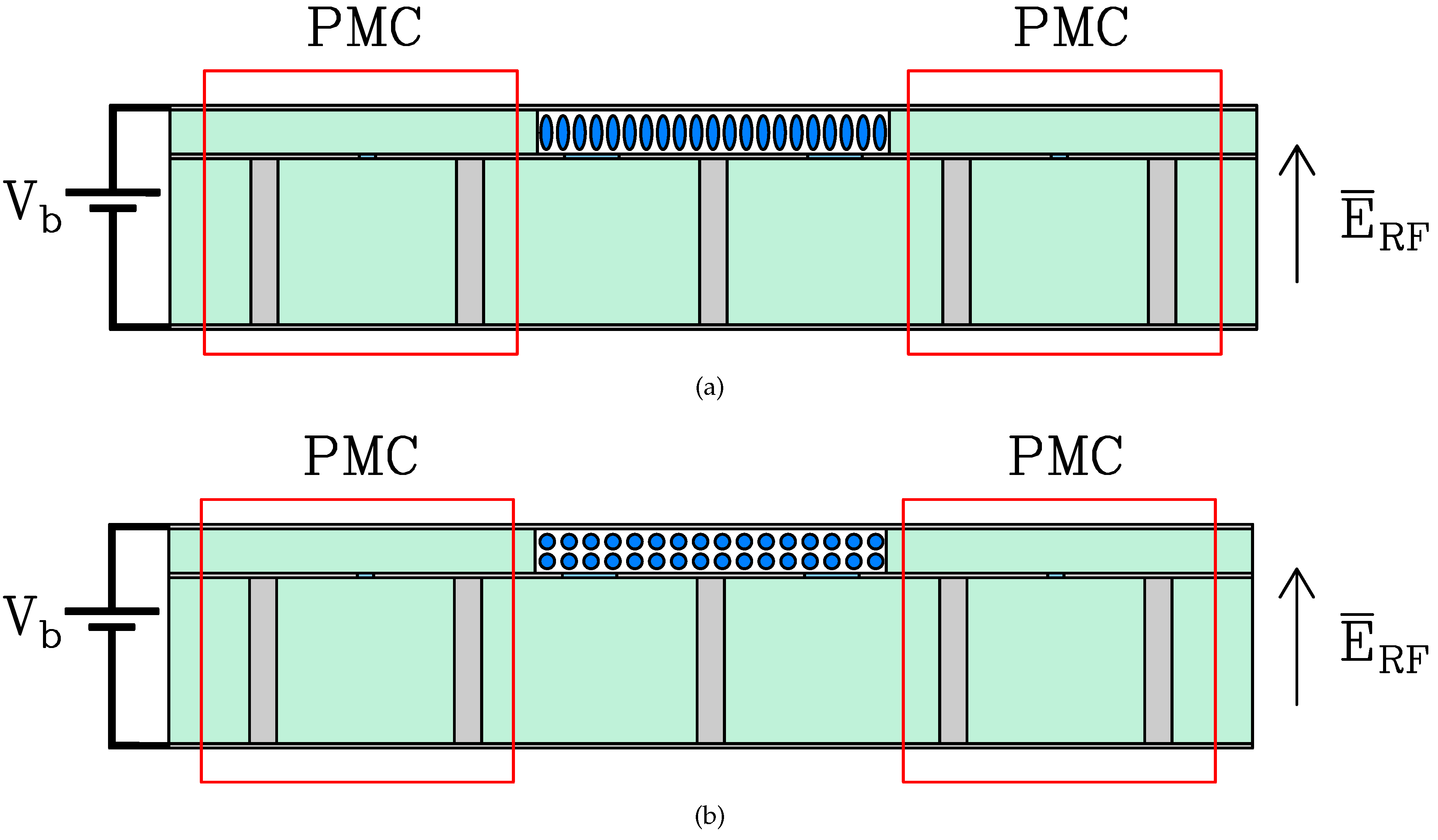
As shown in
Figure 1, which presents the cross section of the phase shifter device described in section 2.5, the LC molecules begin to rotate when the bias voltage applied between the two electrodes exceeds the Fréedericks threshold value [
8]. When the director vector of the LC molecules forms a perpendicular angle to the polarization field, the permittivity of the perpendicular state (
is achieved, as shown in
Figure 1, (b). The threshold voltage
depends on the elastic constant of extension
and the electrical anisotropy
, as shown in Equation (
1). As
increases, it reaches the saturation state (
), resulting in the LC molecules being fully aligned to the parallel state and thus achieving the parallel permittivity
,
Figure 1, (a). On the other hand, when the bias voltage exceeds the Fréedericks threshold (
) intermediate permittivity values between the two extreme states
and
can be achieved.
In this work, nematic liquid crystals’ mixtures will be used from the company MERCK, specifically the models "GT3-23002" and "GT7-29001". The LC’s EM properties given by the manufacturer and measured at 19 GHz: dielectric constant and loss tangent are resumed in
Table 1. Last but not least, it is necessary to highlight that PMC which is used to confine the EM field by the LC substrate, are framed in red in
Figure 1, and will be described in the following section.
2.2. Design of a High Impedance Surface
The scatter diagram studies the bandgap that derives from the study of the Floquet-Bloch modes that propagate through a metasurface [
14], in particular and in the context of this work, the HIS which provides the condition of a PMC, [
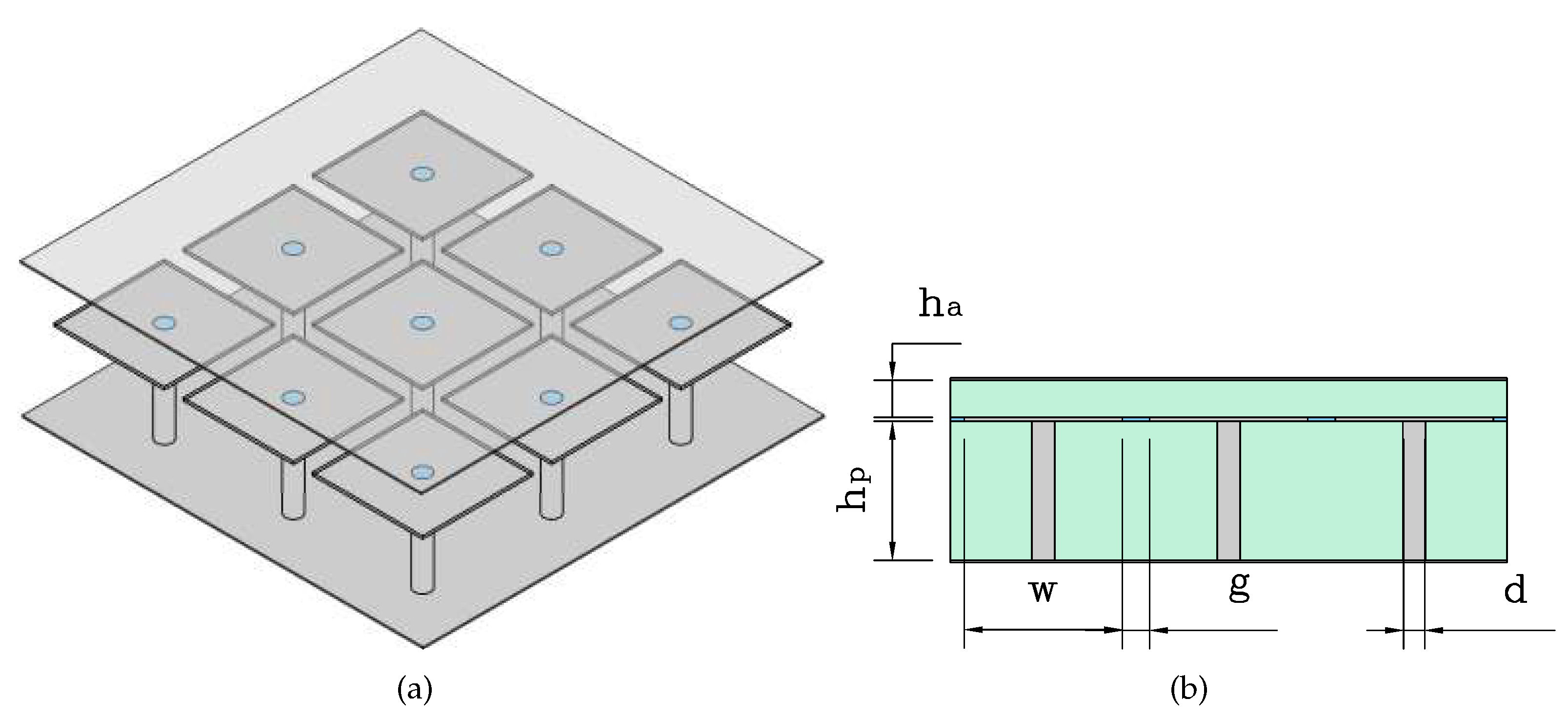
15], is recreated in practice by an array of metallized “mushroom” cells as it can be seen from the
Figure 2.
2.2.1. Parametric Analysis
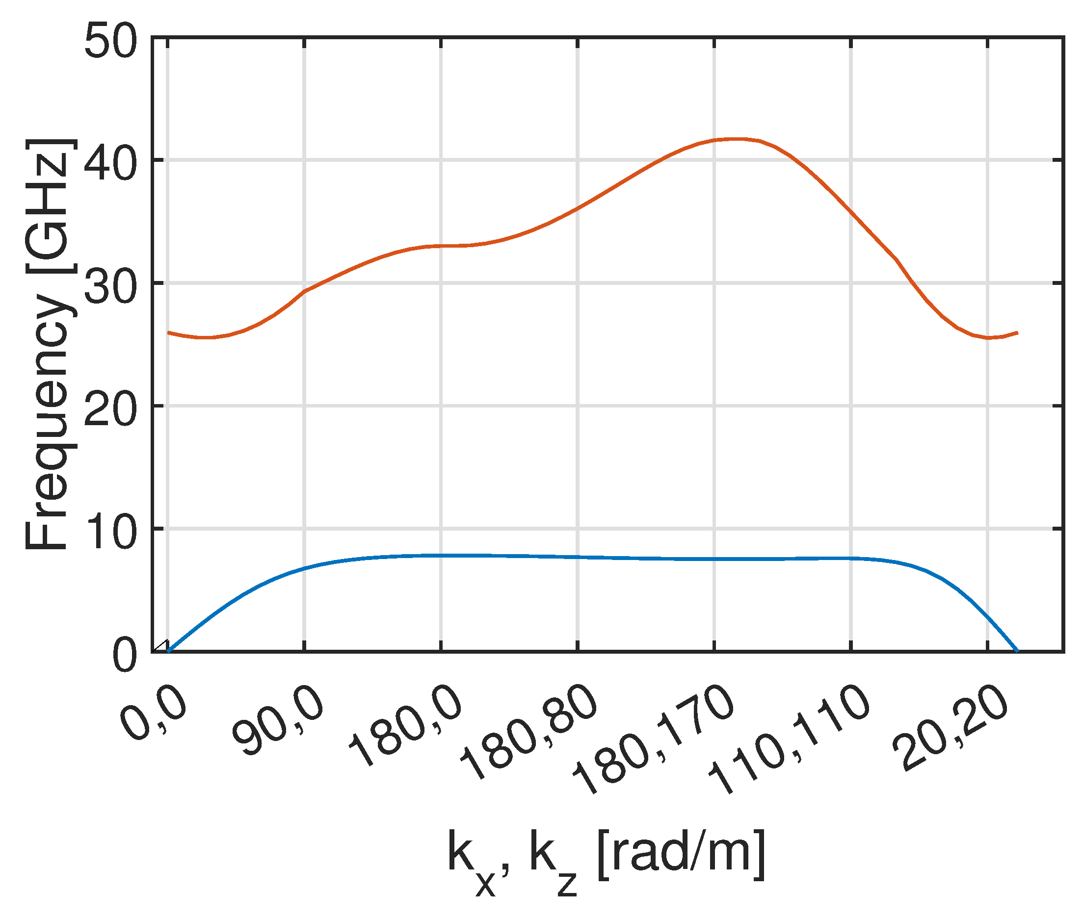
To conduct the parametric analysis of the unit cell, CST Dassault Systems v. 2024 is used. The scatter plot illustrates the propagation constant on the two axes of the two-dimensional matrix (OX, OZ) of the periodically extended "mushroom" base cell,
Figure 3. The bandgap calculation employs the eigenmode solver, which computes the EM field eigenmodes at specific frequencies without external excitation. Dispersion curves are plotted along a specified path, representing waves with various combinations of wave vector components in the OX and OZ directions. Subsequent sections will detail the parameters influencing the frequency range variation of the EM bandgap.
According to [
16], the parameters influencing the response (EM bandgap) of an array of metallic "mushrooms" are as follows:
Diameter of the via (d): affects directly the maximum frequency of both the lower and upper modes (represented by dispersion curves), increasing the resonance frequency. Moreover, since the minimum frequency of the upper mode increases more than that of the lower mode, a wider bandwidth is achieved.
Height of the lower substrate (): affects inversely the maximum frequency of the lower mode. Therefore, increasing the height of the lower substrate increases the bandwidth.
Height of the upper substrate (): affects directly the maximum frequency of the lower mode. Thus, increasing the height of the upper substrate reduces the bandwidth of the EM bandgap.
Material permittivity (): affects directly the maximum frequency of the lower mode, thereby reducing the bandwidth of the EM bandgap.
Patch dimensions (w): affects inversely both the maximum frequency of the lower mode and the minimum frequency of the upper mode of the EM bandgap. However, since the maximum frequency of the lower mode increases less than the minimum frequency of the upper mode, the bandwidth of the EM bandgap is widened.
The frequency range required for the proper reconfiguration of the passband for MRGW-CL devices is from 7 GHz to 20 GHz. The two substrates used are RO4003C with a permittivity of 3.55, where the height of the lower substrate is mm and the height of the upper substrate is mm.
A parametric design was conducted using CST Dassault Systems v. 2024. The periodic design was studied using the eigenmode solver tool, as shown in Figure , and Figure , along the OX and OZ axes. For the OY axis, perfect electric conductor boundary conditions were specified. By varying the field vectors
and
, dispersion curves along with the EM bandgap were calculated, as illustrated in
Figure 3.
After successive iterations, a EM bandgap between 7 GHz and 25 GHz was achieved. The final design, along with the design parameters, is presented in
Table 2.
2.3. Proposed Coupling Network
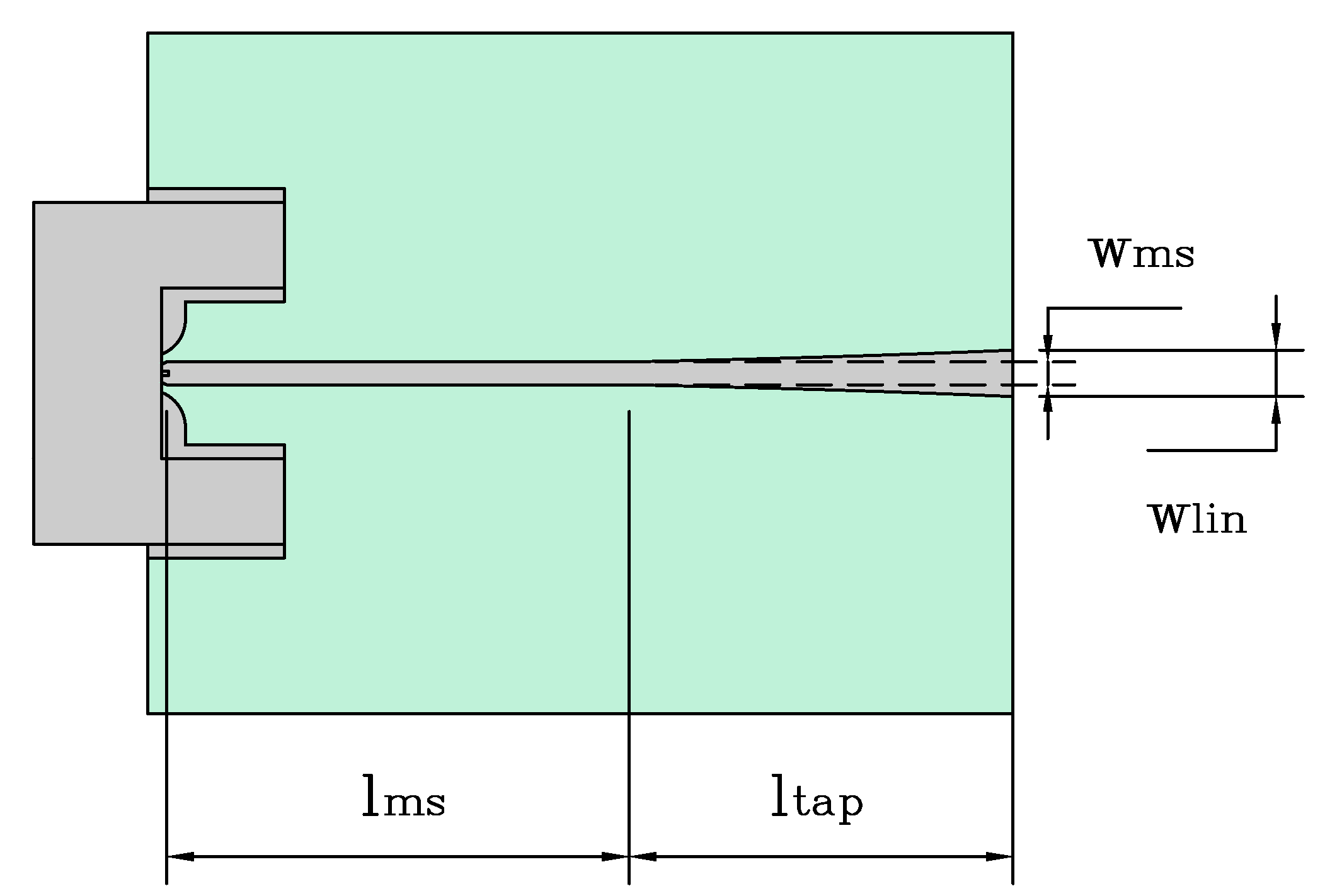
The complete design includes a matching network between the coaxial cable and the device under test (DUT). The “1092-01A-6 Southwest” connector has been chosen to match the coaxial cable to the microstrip line. Additionally, the matching network includes an exponential taper to match the 50
microstrip line input impedance to the 35
MRGW-LC circuit impedance (of phase shifter or stub resonator),
Figure 4, the line widths are
and
accordingly.
2.3.1. Impedance Approximation Using a Stripline Equivalence
To theoretically determine the characteristic impedance of the MRGW-LC line, the characteristic impedance of the model implemented using stripline technology is first established, and the line width is then derived from this model. Finally, the width of the MRGW line is calculated based on the width of the equivalent stripline model, [
17].
An equivalence can be established between the MRGW line and the stripline, as shown in Equation (
2).
And, therefore, it can be assumed that for the same characteristic impedance, the following holds true, Equation (
3).
The width of the stripline given the characteristic impedance remains to be calculated. It is determined as follows in Equation (
4).
2.4. Calibration Kit Design
In order to exclude the effect of the feeding network, from the microstrip section to the exponential taper section (regarding insertion losses, phase, etc.) when measuring S-parameters with a VNA, a TRL calibration kit has been designed considering the following aspects, [
17]:
Reflect: the length of the microstrip section is used, leaving approximately 10 mm spacing between open sections.
Thru: is twice the length of the microstrip line is used.
Line: is approximately 90º of electrical length is added.
Additionally, for the initial measurements and to validate the manufactured TRL calibration kit, a TOSM calibration kit (Through – Open – Short – Match) with reference "Agilent 85052D" was used.
Figure 5 presents the top view of the TRL kit with dimensions, and
Table 3 summarizes the parameters of the final design.
2.5. Proposed MRGW-LC Phase Shifter
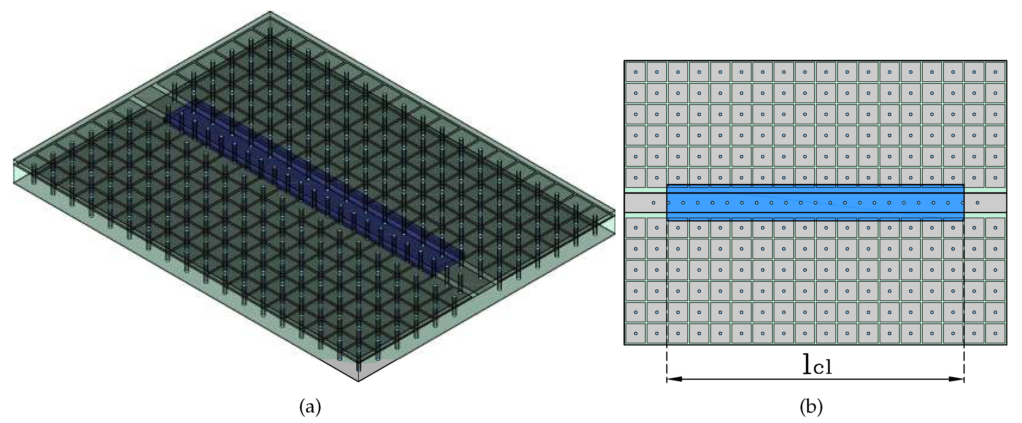
The design is structured into three layers, implemented using three PCBs. Where the LC bathtub is formed by internal cutting of the upper substrate. The LC filled cavity occupies a length of approximately two wavelengths at 11 GHz,
. This length was chosen to provide a clearer comparison between the MRGW filled and unfilled devices. The device’s topology is given by
Figure 6.
2.6. Proposed MRGW-LC Stub Resonator
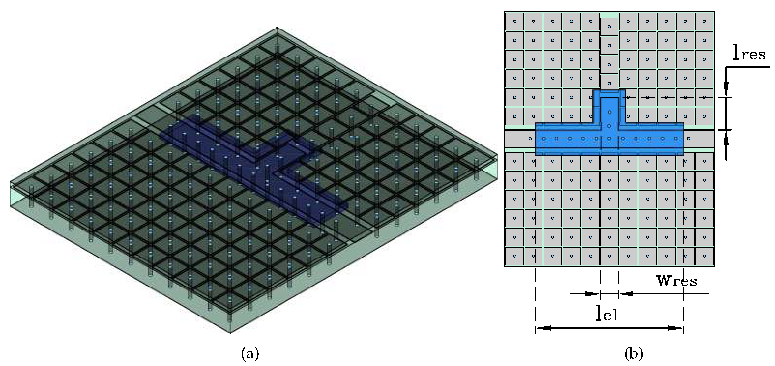
Since the resonator extends half the wavelength, [
18], and by evaluating a phase shifter device with any length in CST Dassault Systems v. 2024, the effective wavelength is determined by simulating the model and consequently the resonator’s cavity extension is determined. Finaly, the model is evaluated and the results are presented in
Table 4, the topology is given by
Figure 7.
2.7. Alignment Layer
The alignment coating is typically formed by depositing poliimide (PI), a polymeric resin composed of repetitive imide units, on the liquid crystal support, usually glass, followed by creating microgrooves through rubbing in a defined direction. However, when applying this layer on a rougher substrate such as copper, the significant surface roughness can obscure the microgrooves of the alignment layer, potentially causing malfunction. In such cases, a thicker layer of PI is commonly used, [
19,
20].
2.7.1. Poliimide Deposition
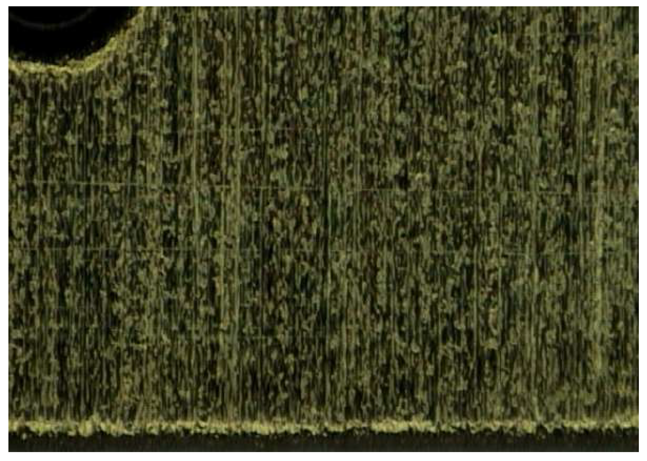
The PI is applied using a pipette onto the circuit and distributed via spin coating. Prior to this, a Kapton mask is used to prevent PI deposition on the “mushroom” bed. This procedure produces a uniform layer approximately 500 nm thick. The initial curing is performed at 80 °C for 20 minutes, followed by a second curing at 180 °C for 1 hour, next Kapton mask was removed by carefully cutting around the edges of the masking tape. As a result, the samples were covered and allowed to rest for a couple of hours and subsequently velvet rubbing was performed to create the microgrooves of the alignment layer. Finally, to ensure that the rubbing process has created grooves, a microscope was used to perform measurements. It is confirmed that fine microgrooves have been created on the alignment layer, as observed in
Figure 8.
2.8. Assembling and Filling
The three layers of the MRGW-LC devices were assembled by welding and screwing. A low-temperature, no-clean solder paste (SMDLTLFP10T5 from Chipquik) was used to assemble the stack. "1092-01A-6 Southwest" 2.92mm female coax connectors for the RF signal were screwed to the ports, Bias Tee (SHF BT45-R) to couple the DC electrical signal together with the RF electrical signal was used. The frequency response (transmission
and reflection
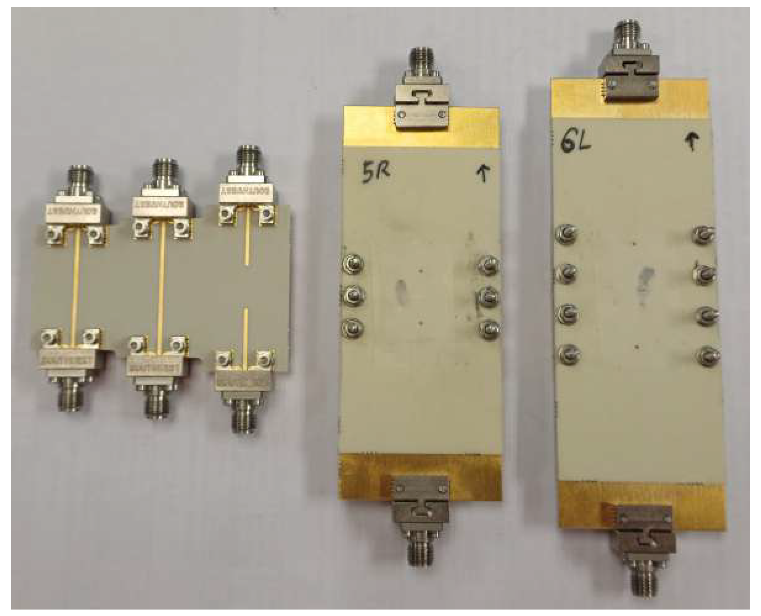
parameters) of the empty MRGW-LC devices were measured to verify proper device functionality, Figure 11. The MRGW-LC’s devices were then filled with GT3-23002 and GT7-29001 liquid crystals using a syringe and sealed with NOA-61 optical glue. The assembled devices and the TRL calibration kit are presented in
Figure 9.
2.9. Measurement Setup
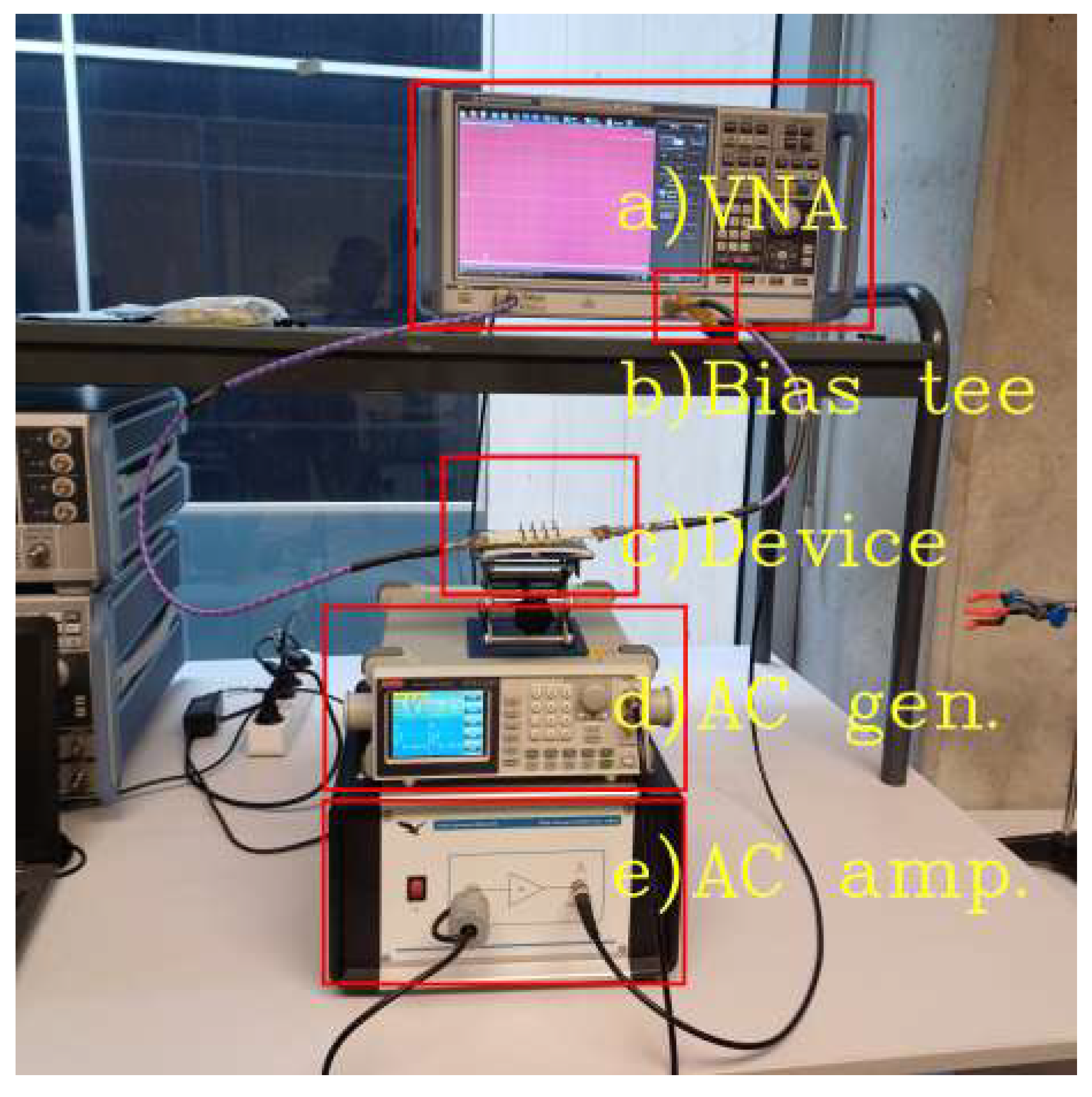
The measurement setup required a low-frequency signal generator and an AC voltage amplifier to generate the bias signal and a sinusoidal wave of 1 kHz, which was varied from 0 to 125
during the measurement. The amplified low-frequency signal is then fed to bias tee, which combines it with RF signal from a Vectorial Network Analyzer (VNA). The frequency response of the resonator was measured at different bias voltages using a VNA with additional DC blocks to protect the equipment.
Figure 10 shows the whole measurement setup.
3. Results And Discussion
The electrical response of the MRGW-LC devices used in this study lacks a theoretical solution due to their complex structure and multiple dielectric materials (RO4003 substrate and LC). Therefore, the structure was simulated using the commercial software CST Dassault Systems v. 2024, and the electrical properties of the liquid crystal were computed accordingly.
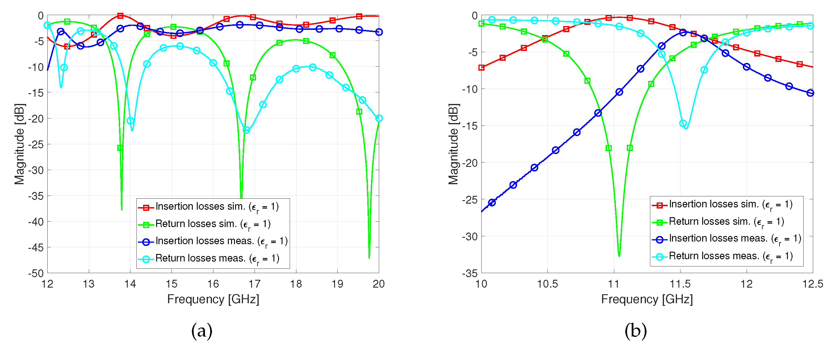
Firstly, in order to ensure that the manufactured devices agree with the simulation results, measurements were made in a vacuum, without filling the devices with LC, as shown in
Figure 11. It is necessary to remark at this point, that phase shifter device’s frequency response has a good agreement with the simulated response. However the resonator device’s response, in comparison to the simulated one, is shifted from
towards
due to manufacturing tolerances.
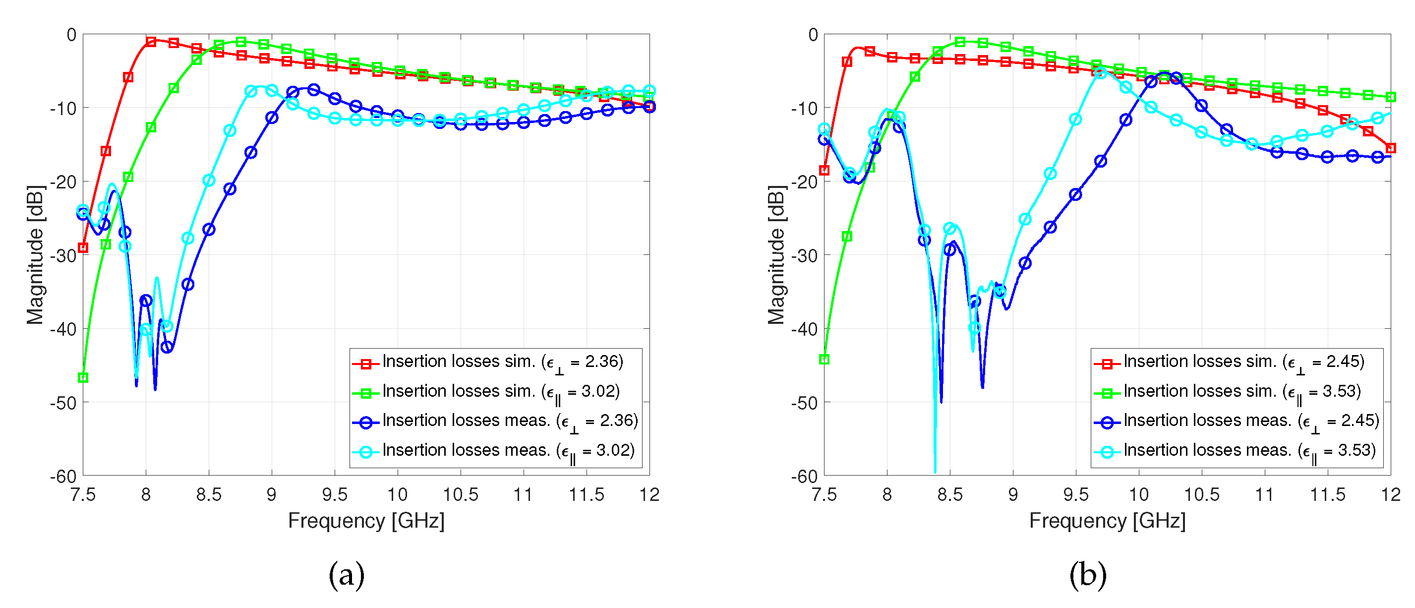
Secondly, the devices were filled with GT3-23002 and GT7-29001 and the measurements were performed. The analytical results obtained through simulation are compared with this measurements and the conclusions are drawn. As can be seen from the
Figure 12, the measured reconfigurability range of GT3-23002 is of 4.08% (
and
) and of GT7-29001 is 4.82% (
and
). In contrast, the simulated reconfigurability range of GT3-23002 is of 7.60%(
and
) and of GT7-29001 is 10.72% (
and
). As it can be deduced from the results, it is noticeable that the resonator is not completely filled, as it can be seen from the shift in the perpendicular state frequency.
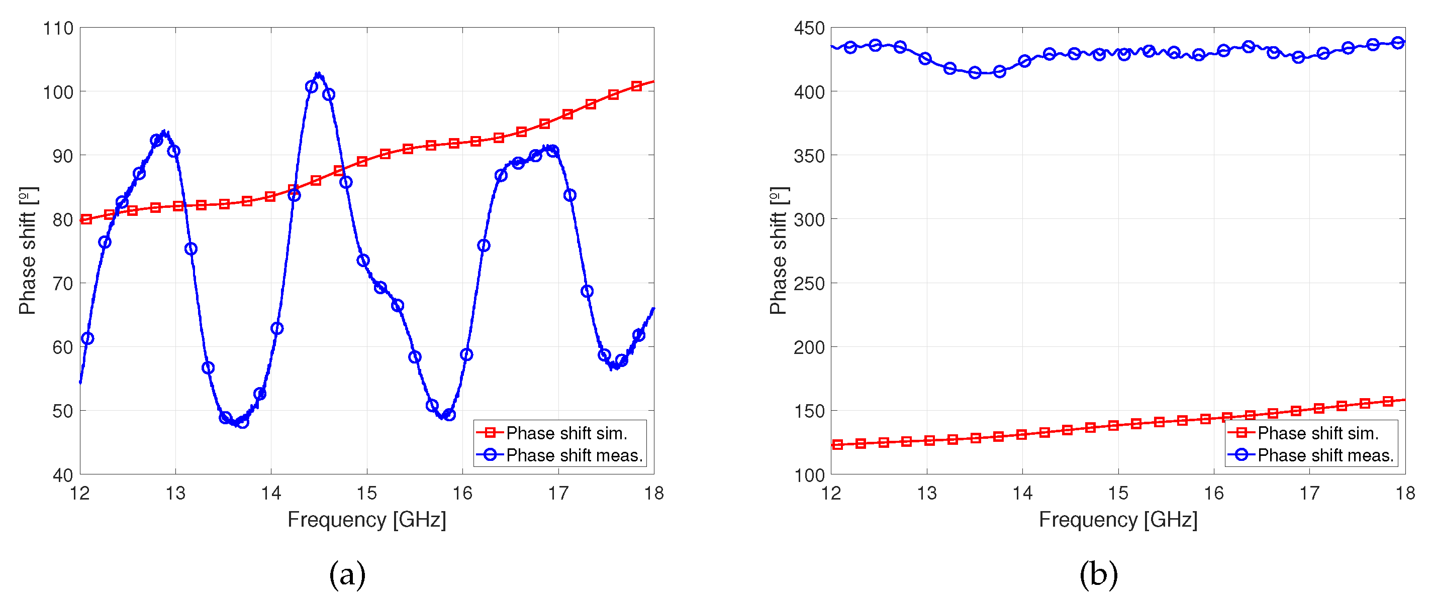
For the phase shifter devices,
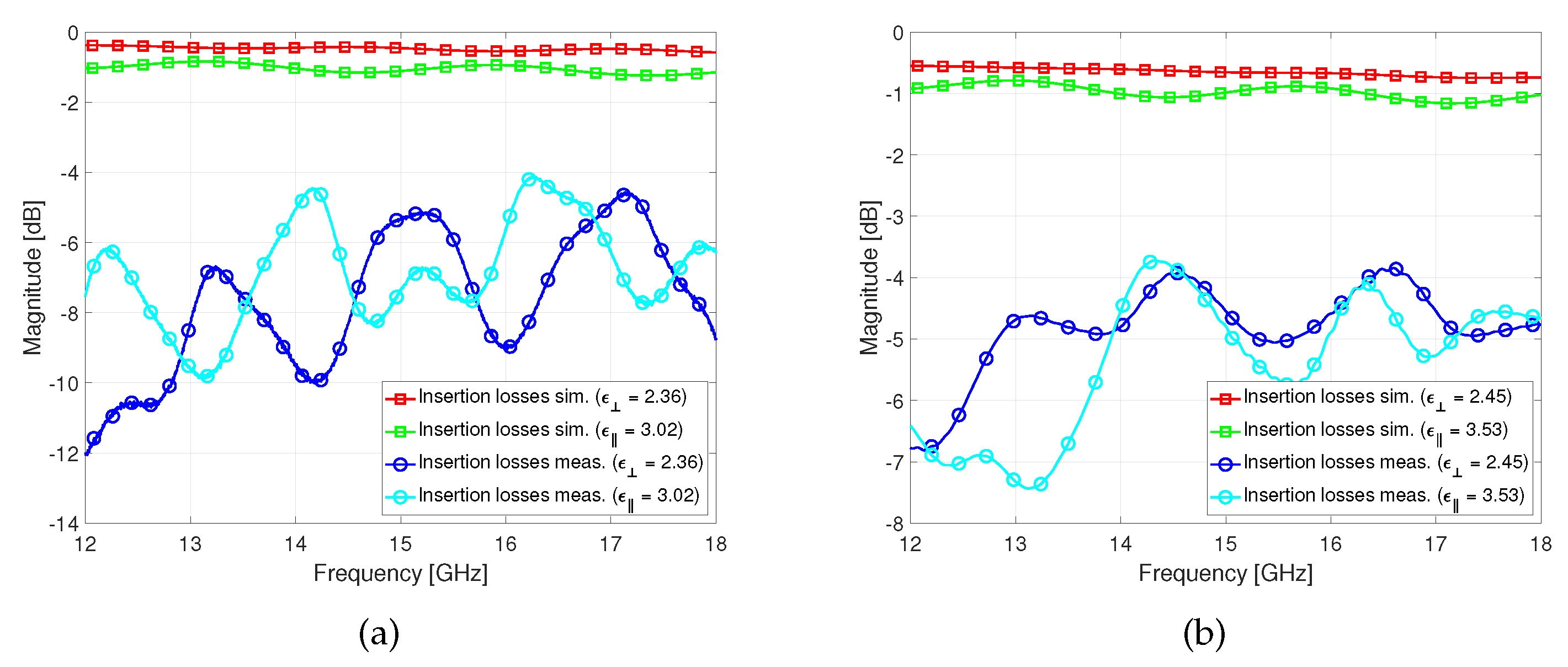
Figure 13 clearly shows that the phase shift results of the GT3-23002 fit well with the simulation, following a periodic pattern with the mean of approximately 75º of phase shift. Similarly, the measured phase pattern of the GT7-29001, exhibits a linear trend similar to the simulated one, but with a noticeable increase in phase shift. The GT3-23002 as well as GT7-29001 filled devices exhibit significant insertion losses compared to the simulated ones,
Figure 14, although GT7-29001 phase shifter presents generally less insertion losses.
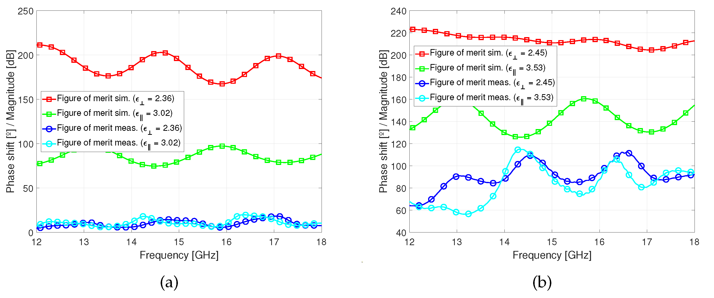
We define Figure of Merit (FoM) as the maximum ratio of the phase shift and the insertion loss. Thus, both perpendicular state and parallel state FoM are computed and measured,
Figure 14. It is clearly seen that due to high insertion losses,
Figure 15, the phase shifter measured with GT3-23002 presents the mean of 10º per every 1 dB of losses in both perpendicular and parallel states; nevertheless the phase shifter measured with GT7-29001 presents the mean of 84º for parallel state and 92º for perpendicular state per every 1 dB of losses.
4. Conclusions
The aim of this work is to develop miniaturized microwave devices using a new substrate-integrated waveguide technology with the suppression of traveling surface waves combined with functional materials that allow frequency reconfigurability. The phase shifter and resonator devices are developed and manufactured by layers conforming the cavities which are coated with alignment layers and consequently sealed with NOA-61 optical adhesive to guarantee that the devices are waterproof and then filled with two commercial liquid crystal mixtures (GT3-23002 and GT7-29001 from MERCK).
The devices are then fed by an RF signal coupled with the variable bias voltage to measure their electric response, then valuable results are extracted. Although the measurements of frequency response, phase shift and FoM of two of the liquid crystals’ mixtures were achieved, there are challenges that have been discovered, mainly the devices’ waterproofing due to LC’s leakage. This problem should be addressed in order to guarantee that the DUT remains filled and waterproof so as to obtain results of better quality. As a result, the development of compact devices based on MRGW-LC will allow the integration of microwave devices with LC’s if these problems are overcome.
Author Contributions
Conceptualization, C.B. and A.V.; methodology, C.B.; software, A.V.; validation, C.B., V.B. and A.V.; formal analysis, C.B. and A.V.; investigation, C.B., B.V. and A.V.; resources, B.V.; data curation, A.V.; writing—original draft preparation, A.V.; writing—review and editing, A.V. and C.B.; visualization, A.V.; supervision, C.B.; project administration, A.V. and C.B.; funding acquisition, V.B. All authors have read and agreed to the published version of the manuscript.
Abbreviations
The following abbreviations are used in this manuscript:
| LC |
Liquid Crystal |
| MRGW |
Microstrip Ridge Gap Waveguide |
| MRGW-LC |
Microstrip Ridge Gap Waveguide with Liquid Crystal |
| RF |
Radio Frequency |
| MEMS |
Microelectromechanical Systems |
| FoM |
Figure of Merit |
| PMC |
Perfect Magnetic Conductor |
| EM |
Electromagnetic |
| PCB |
Printed Board Circuits |
| DC |
Direct Current |
| PI |
Polyimide |
| AC |
Alternate Current |
| HIS |
High Impedance Surface |
| VNA |
Vectorial Network Analyzer |
| DUT |
Device Under Test |
References
- Monserrat, J.F.; Martin-Sacristan, D.; Bouchmal, F.; Carrasco, O.; Flores de Valgas, J.; Cardona, N. Key Technologies for the Advent of the 6G. 2020 IEEE Wireless Communications and Networking Conference Workshops (WCNCW), 2020, pp. 1–6. [CrossRef]
- Xiao, M.; Mumtaz, S.; Huang, Y.; Dai, L.; Li, Y.; Matthaiou, M.; Karagiannidis, G.K.; Björnson, E.; Yang, K.; I, C.L.; Ghosh, A. Millimeter Wave Communications for Future Mobile Networks. IEEE Journal on Selected Areas in Communications 2017, 35, 1909–1935. [Google Scholar] [CrossRef]
- 5G Mobile and Wireless Communications Technology; Cambridge University Press, 2016.
- Tataria, H.; Shafi, M.; Molisch, A.F.; Dohler, M.; Sjöland, H.; Tufvesson, F. 6G Wireless Systems: Vision, Requirements, Challenges, Insights, and Opportunities, 2021.
- Reconfigurable Circuits and Technologies for Smart Millimeter-Wave Systems; EuMA High Frequency Technologies Series, Cambridge University Press, 2022.
- Herrick, K.; Yook, J.; Katehi, L. Microtechnology in the development of three-dimensional circuits. IEEE Transactions on Microwave Theory and Techniques 1998, 46, 1832–1844. [Google Scholar] [CrossRef]
- Kildal, P.S.; Alfonso, E.; Valero-Nogueira, A.; Rajo-Iglesias, E. Local Metamaterial-Based Waveguides in Gaps Between Parallel Metal Plates. IEEE Antennas and Wireless Propagation Letters 2009, 8, 84–87. [Google Scholar] [CrossRef]
- Wu, S.; Yang, D.K. Fundamentals of Liquid Crystal Devices. 2006.
- Reese, R.; Polat, E.; Tesmer, H.; Strobl, J.; Schuster, C.; Nickel, M.; Granja, A.B.; Jakoby, R.; Maune, H. Liquid Crystal Based Dielectric Waveguide Phase Shifters for Phased Arrays at W-Band. IEEE Access 2019, 7, 127032–127041. [Google Scholar] [CrossRef]
- Muller, S.; Scheele, P.; Weil, C.; Wittek, M.; Hock, C.; Jakoby, R. Tunable passive phase shifter for microwave applications using highly anisotropic liquid crystals. 2004 IEEE MTT-S International Microwave Symposium Digest (IEEE Cat. No.04CH37535), 2004, Vol. 2, pp. 1153–1156 Vol.2. [CrossRef]
- Weil, C.; Luessem, G.; Jakoby, R. Tunable inverted-microstrip phase shifter device using nematic liquid crystals. 2002 IEEE MTT-S International Microwave Symposium Digest (Cat. No.02CH37278), 2002, Vol. 1, pp. 367–371 vol.1. [CrossRef]
- Liu, Y.; Jiang, D.; Li, X.; Wang, Z.; Ran, P.; Fu, Z. Microwave CSIW Filter Based on The High Anisotropy Electro-Optic Nematic Liquid Crystal. 2019 International Conference on Microwave and Millimeter Wave Technology (ICMMT), 2019, pp. 1–3. [CrossRef]
- Polat, E.; Reese, R.; Jost, M.; Schuster, C.; Nickel, M.; Jakoby, R.; Maune, H. Tunable Liquid Crystal Filter in Nonradiative Dielectric Waveguide Technology at 60 GHz. IEEE Microwave and Wireless Components Letters 2019, 29, 44–46. [Google Scholar] [CrossRef]
- Brillouin, L. Wave Propagation In Periodic Structures Electric Filters And Crystal Lattices; McGraw-Hill, 1946.
- Sievenpiper, D.; Zhang, L.; Broas, R.; Alexopolous, N.; Yablonovitch, E. High-impedance electromagnetic surfaces with a forbidden frequency band. IEEE Transactions on Microwave Theory and Techniques 1999, 47, 2059–2074. [Google Scholar] [CrossRef]
- Palomar Cosín, E. Diseño e implementación de una línea Gap Ridge Waveguide integrada en sustrato con cristal líquido. B.s. thesis, 2021.
- Alfonso, E.; Kildal, P.S.; Valero-Nogueira, A.; Baquero, M. Study of the characteristic impedance of a ridge gap waveguide. 2009 IEEE Antennas and Propagation Society International Symposium, 2009, pp. 1–4. [CrossRef]
- Pozar, D. Microwave Engineering; Wiley, 2012.
- Zografopoulos, D.C.; Ferraro, A.; Beccherelli, R. Liquid-Crystal High-Frequency Microwave Technology: Materials and Characterization. Advanced Materials Technologies 2019, 4, 1800447. [Google Scholar] [CrossRef]
- Yazdanpanahi, M.; Bulja, S.; Mirshekar-Syahkal, D.; James, R.; Day, S.E.; Fernandez, F.A. Measurement of Dielectric Constants of Nematic Liquid Crystals at mm-Wave Frequencies Using Patch Resonator. IEEE Transactions on Instrumentation and Measurement 2010, 59, 3079–3085. [Google Scholar] [CrossRef]
Figure 1.
Polarization of the CL in the nematic state (a) (b) .
Figure 1.
Polarization of the CL in the nematic state (a) (b) .
Figure 2.
High impedance surface: (a) array of "mushroom" cells, (b) transversal cut of an array of "mushroom" cells.
Figure 2.
High impedance surface: (a) array of "mushroom" cells, (b) transversal cut of an array of "mushroom" cells.
Figure 3.
The scatter plot of HIS.
Figure 3.
The scatter plot of HIS.
Figure 4.
MRGW-LC’s coupling network.
Figure 4.
MRGW-LC’s coupling network.
Figure 5.
TRL calibration kit: (a) open, (b) line, (b) thru.
Figure 5.
TRL calibration kit: (a) open, (b) line, (b) thru.
Figure 6.
MRGW-LC phase shifter: (a) isometric view, (b) top view.
Figure 6.
MRGW-LC phase shifter: (a) isometric view, (b) top view.
Figure 7.
MRGW-LC phase shifter: (a) isometric view (b) top view.
Figure 7.
MRGW-LC phase shifter: (a) isometric view (b) top view.
Figure 8.
MRGW-LC device’s microgrooves.
Figure 8.
MRGW-LC device’s microgrooves.
Figure 9.
MRGW-LC devices (from left to right): TRL calibration kit, stub resonator, phase shifter.
Figure 9.
MRGW-LC devices (from left to right): TRL calibration kit, stub resonator, phase shifter.
Figure 10.
Measurement setup: a) Vectorial Network Analyzer (VNA), (b) bias tee, (c) device under test, d) AC signal generator, e) AC voltage amplifier.
Figure 10.
Measurement setup: a) Vectorial Network Analyzer (VNA), (b) bias tee, (c) device under test, d) AC signal generator, e) AC voltage amplifier.
Figure 11.
MRGW-LC devices’ frequency response measured in vacuum: (a) phase shifter, (b) stub resonator.
Figure 11.
MRGW-LC devices’ frequency response measured in vacuum: (a) phase shifter, (b) stub resonator.
Figure 12.
Frequency response comparison of the simulated and measured response of the resonator filled with: (a) GT3-23002, (b) GT7-29001.
Figure 12.
Frequency response comparison of the simulated and measured response of the resonator filled with: (a) GT3-23002, (b) GT7-29001.
Figure 13.
Phase shift comparison of the simulated and measured response of the phase shifter filled with: (a) GT3-23002, (b) GT7-29001.
Figure 13.
Phase shift comparison of the simulated and measured response of the phase shifter filled with: (a) GT3-23002, (b) GT7-29001.
Figure 14.
Insertion losses comparison of the simulated and measured response of the phase shifter filled with: (a) GT3-23002, (b) GT7-29001.
Figure 14.
Insertion losses comparison of the simulated and measured response of the phase shifter filled with: (a) GT3-23002, (b) GT7-29001.
Figure 15.
Figure of merit comparison of the simulated and measured response of the phase shifter filled with: (a) GT3-23002, (b) GT7-29001.
Figure 15.
Figure of merit comparison of the simulated and measured response of the phase shifter filled with: (a) GT3-23002, (b) GT7-29001.
Table 1.
EM properties of commercial LC’s mixtures measured at 19 GHz.
Table 1.
EM properties of commercial LC’s mixtures measured at 19 GHz.
| |
GT3-23002 |
GT7-29001 |
|
3.02 |
3.53 |
|
2.36 |
2.45 |
|
0.0035 |
0.0064 |
|
0.0128 |
0.00117 |
Table 2.
HIS’s design parameters.
Table 2.
HIS’s design parameters.
| Parameter |
Value [mm] |
|
0.406 |
|
1.524 |
| g |
0.300 |
| w |
1.734 |
| d |
0.250 |
Table 3.
TRL calibration kit’s design parameters.
Table 3.
TRL calibration kit’s design parameters.
| Parameter |
Value [mm] |
|
31.473 |
|
28.000 |
|
0.300 |
|
1.734 |
Table 4.
HIS’s design parameters.
Table 4.
HIS’s design parameters.
| Parameter |
Value [mm] |
|
3.247 |
|
1.728 |
|
14.669 |
|
Disclaimer/Publisher’s Note: The statements, opinions and data contained in all publications are solely those of the individual author(s) and contributor(s) and not of MDPI and/or the editor(s). MDPI and/or the editor(s) disclaim responsibility for any injury to people or property resulting from any ideas, methods, instructions or products referred to in the content. |
© 2024 by the authors. Licensee MDPI, Basel, Switzerland. This article is an open access article distributed under the terms and conditions of the Creative Commons Attribution (CC BY) license (http://creativecommons.org/licenses/by/4.0/).
