1. Introduction
With the continuous evolution of modern optoelectronic technology, there is a notable trend towards the integration and miniaturization of specialized optical systems. micro lens arrays(MLAs), recognized as significant optical components, offer advantages such as compactness, lightweight design, multifunctionality and high integration capability [
1,
2,
3]. They find applications across various domains including optical imaging [
4,
5,
6], new energy technologies [
7,
8] and advanced display systems [
9,
10].
In the field of advanced technological applications, the fabrication techniques for MLA have been posed increasingly stringent demands. Traditional methods for MLA fabrication include photolithography [
11,
12,
13], thermal reflow [
14], electron beam lithography [
15], and self-assembly [
16]. However, photolithography and electron beam lithography are costly, complex in process, and inefficient in production. Thermal reflow exhibits poor flexibility, low processing precision, complex procedures, and primarily applicable to polymers [
17,
18]. In contrast, fused silica offers superior chemical stability, mechanical properties, and an extremely low coefficient of thermal expansion compared to materials like polydimethylsiloxane (PDMS) and Polymethyl methacrylate (PMMA). Moreover, it boasts high transparency in the ultraviolet to near-infrared spectrum and exceptionally stable refractive index, making it an ideal material for optical MLA fabrication. Nevertheless, its high stability and hardness present challenges for achieving high-precision processing.
With the development of laser technology, ultrafast lasers have emerged as an effective method for micro/nano fabrication [
19,
20,
21,
22]. Femtosecond (Fs) lasers feature extremely short pulses (~10-15 s), high peak power (1022 W/cm2), and strong controllability. They enable direct writing and material modification within transparent materials [
23]. Utilizing femtosecond lasers to fabricate MLA on silica surfaces is feasible. However, significant surface roughness and low processing speeds have long been challenges in femtosecond laser processing of such brittle materials. Femtosecond laser processing on quartz surfaces often results in substantial roughness and low efficiency, which hinders the creation of high-quality three-dimensional structures. To improve processing efficiency and surface quality, wet etching-assisted femtosecond laser processing has been applied extensively for high-quality surface fabrication and has significantly reduced surface roughness. Currently, a great amount of research suggested that high quality MLA are fabricated by this process [
24,
25].
Although numerous studies have successfully utilized this technique to fabricate MLA with excellent surface quality, challenges remain in achieving size controllability and lack foundational process explorations. In this paper, we proposed a method based on femtosecond laser back facing single-point exposure for material modification, combined with hydrofluoric acid (HF) etching, to achieve controllable fabrication of fused silica MLA efficiently. Through experimental research, two types of MLA fabricated using this method demonstrated excellent imaging capabilities, highlighting the potential applications of this research method in optical imaging and biochemical detection fields.
2. Experiment
2.1. Method and Material
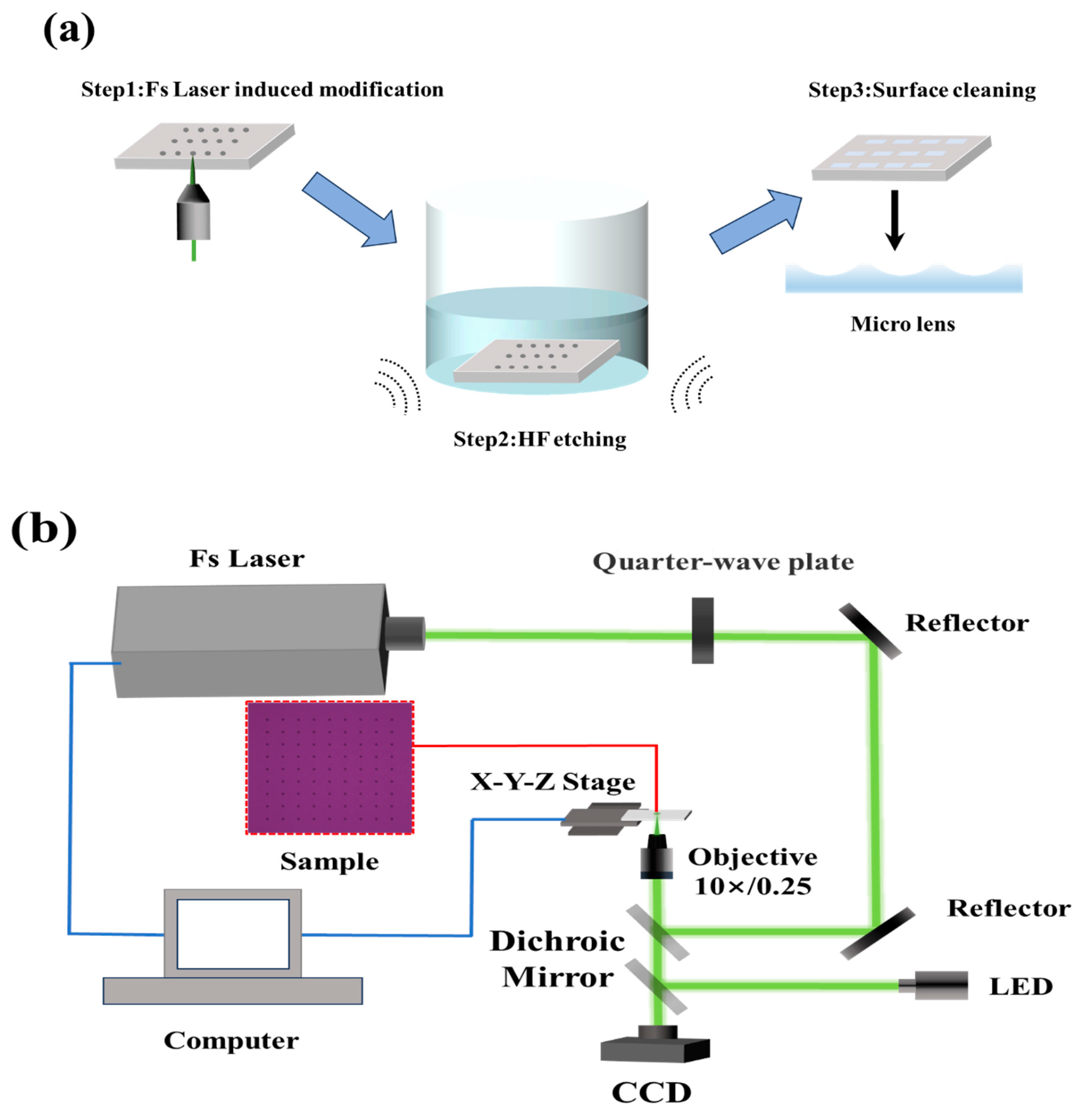
The FLIM-WE preparation method for micro lens array(MLA) mainly includes the following three steps., as shown in
Figure 1(a):.femtosecond-laser-induced modification of fused silica (step 1), wet etching assisted by ultrasonic water bath to remove the modified surface layer(step 2), and subsequent surface cleaning(step 3). Initially, the back facing of fused silica sample underwent induced modification using femtosecond laser single-point exposure, which generated micro lens structures with each exposure. A 20% HF solution was prepared by diluting the original HF solution (40%, AR) with deionized water in a 1:1 ratio. The modified samples were then immersed in the etching solution within a polytetrafluoroethylene container and subjected to wet etching under ultrasonic water bath conditions (ultrasonic power of 80 W, ultrasonic frequency of 40 kHz, water bath temperature of 20°C) to form the final micro lens. Finally, the processed samples was subjected to ultrasonic cleaning to remove residual etching residues.
2.2. Experimental Setup
The experimental setup for femtosecond-laser- induced modification(FLIM) is depicted in
Figure 1(b). Laser beam from the femtosecond laser (laser wavelength of 515 nm, pulse frequency of 25 kHz, pulse width of ~373 fs) passed through a quarter-wave plate, then through a reflection mirror group and a dichroic mirror, and entered into the microscope objective (10×, NA 0.25). The polarization state of the laser beam emitted by the laser is vertical polarization. We rotate the angle of the optical axis of the quarter wave plate to modulate linearly polarized light into circularly polarized light. The light beam focused by the microscope objective traveled from bottom to top, with penetrating the interior of the sample. Then, the focus shifted to the back-facing surface of the sample. A CCD sensor was used for monitoring the laser exposure process and finding the focal plane. The sample moved downwards along the Z-axis. If the CCD observed two focal points, then the plane where the second focal point located is the back facing upper surface to be induced modification. This penetrating induced modification method will effectively avoid the absorption and scattering effects of the modified layer generated by the previous pulse on the subsequent pulse.
We used UV fused silica glass thin plates (0.3mm, the brand of JGS1) in the experiment. This device controlled the laser power used for inducing modification by adjusting the current through a computer. At the same time, the computer coordinated the motion X-Y-Z stage to adjust the pulse state of the emitted laser through the phase sensitive optical (PSO) function. The PSO control system manages the number of pulses, while the motion X-Y-Z stage moving to expose different-sized micro lens on the sample.
Characterization of the fabricated micro lens morphology was performed using a laser confocal microscope (Keyence, VK-X200). The HF solution etching process lasted for 150 minutes, with samples retrieved for morphology observation and analysis every 60 minutes.
3. Results and Discussion
3.1. The Influence of Laser Parameters
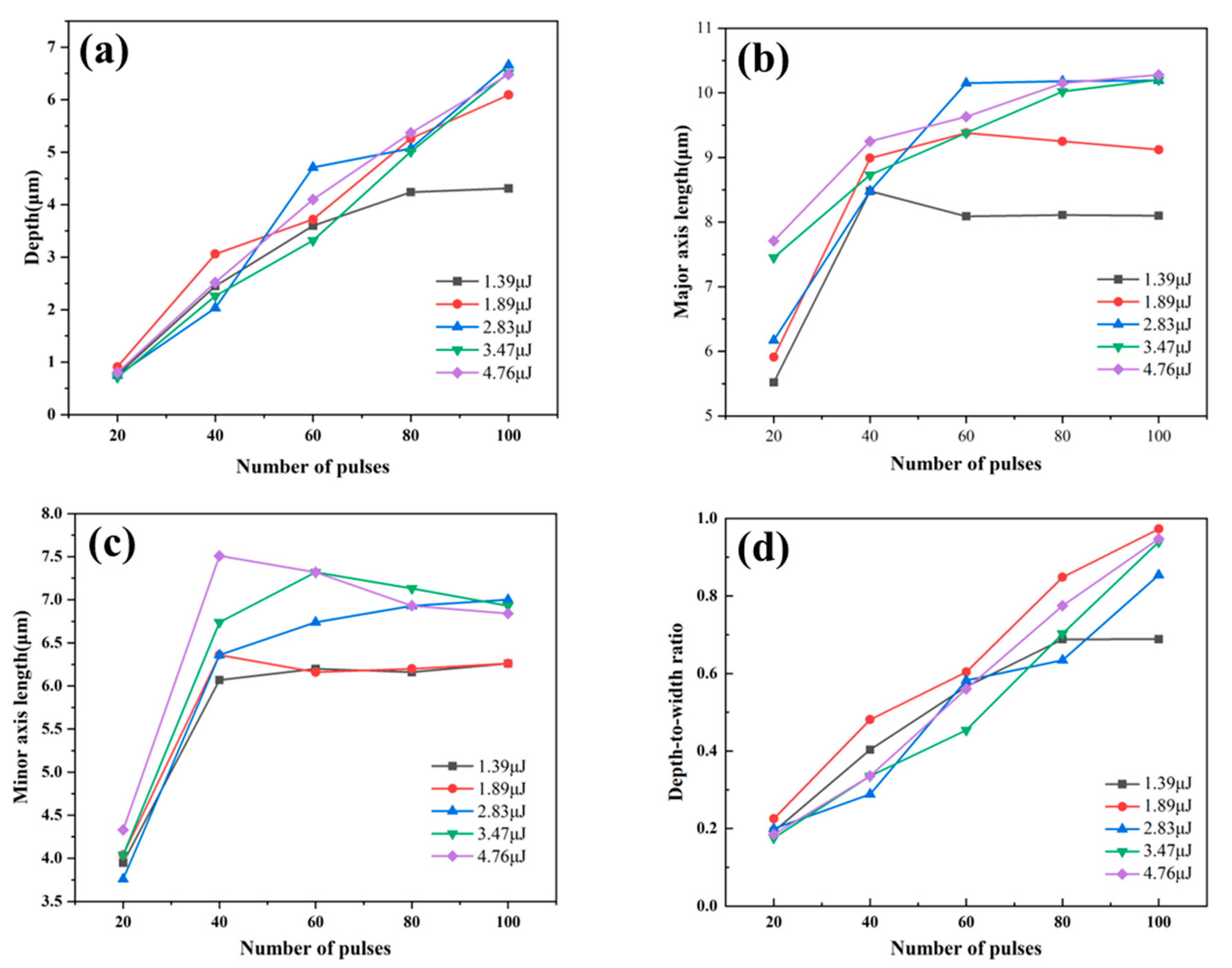
We investigated the impact of varying the number of laser pulse (20-100 pulses) and the energy during the manufacturing process of micro lens on fused silica surfaces, and presented our findings in
Figure 2. Initially, the micro lens formed are elliptical in shape, with the minor and major axes lengths represented on the vertical axes of
Figure 2(b) and
Figure 2(c), respectively.
Figure 2(a) illustrates that under identical energy conditions, the etching depth of the micro lens increases notably with higher pulse counts. Furthermore, with elevated pulse energies, the rate of etching depth augmentation also escalates proportionally. However, at a single pulse energy of 1.39 μJ, minimal changes in etching depth are observed, whereas at 1.89 μJ, the depth increases sharply from 0.91 μm to 6.09 μm with an increasing pulse count. Nevertheless, the maximum etching depth does not escalate indefinitely with higher pulse numbers. Even with a pulse energy increase to approximately 2.5 times (up to 4.76 μJ) at 100 pulses, the etching depth only marginally increased from 6.0 μm to 6.8 μm.
Figure 2(b) and (c) depict that when the pulse count is below 40, both the major and minor axis lengths of the micro lens significantly increase with additional pulses. However, beyond 40 pulses, these dimensions stabilize. This phenomenon can be attributed to the widening of the micro-hole surface area, where the laser edge energy falls below the material ablation threshold, thereby reducing the fused silica removal capability. Consequently, further dimensional changes cease despite continued laser exposure on the fused silica pits.
Figure 2(d) reveals that at a single pulse energy of 1.39 μJ, when the number of pulses is less than 80, the depth to diameter ratio of the microlens increases linearly with the pulse count. While micro lens fabricated with 80 and 100 pulses exhibit nearly identical depth-to-diameter ratios, approximately 0.69. At higher single pulse energies of 1.89 μJ and above, the depth-to-diameter ratio also increases linearly with the pulse count, approaching 0.9 at 100 pulses. However, a larger depth-to-diameter ratio for micro lens implies reduced curvature, leading to diminished magnification in microscopic imaging and increased distortion of the original image. Addressing these challenges may necessitate additional optical design strategies to mitigate substantial distortion effects [
26].
In conclusion, considering these observations comprehensively, our study advocates for employing lower pulse energies and moderate pulse numbers in the fabrication of MLAs.
3.2. Impact of Wet Etching Time
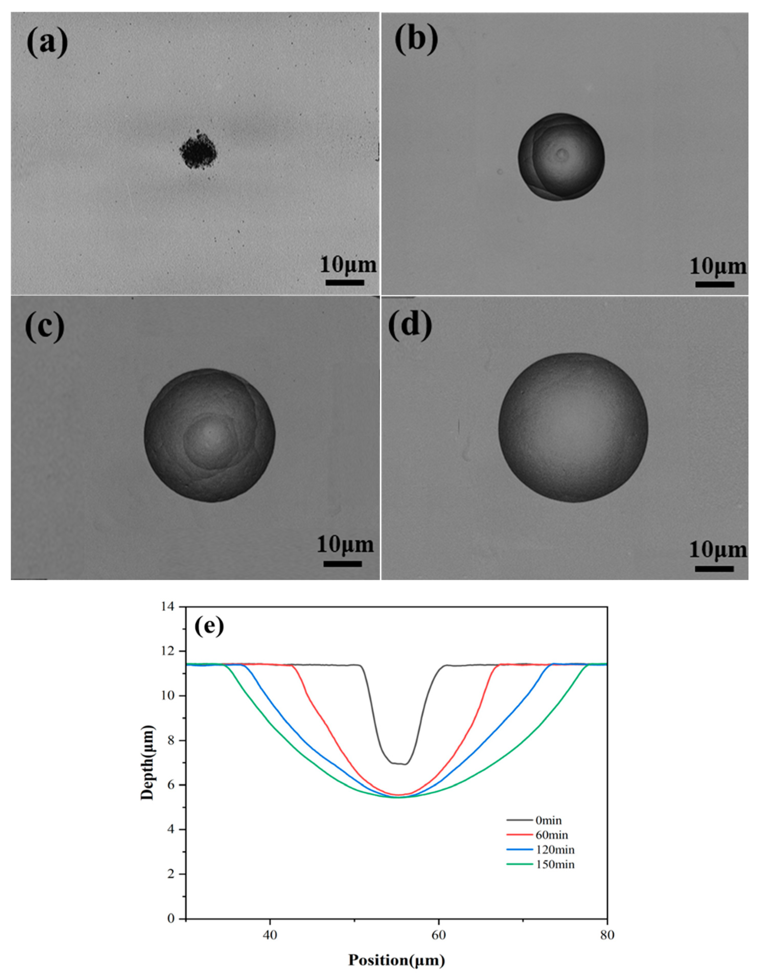
According to Step 2, we studied the influence of HF solution etching time on the dimensions and surface quality of micro lens. Using a femtosecond laser with a single pulse energy of 1.39 μJ and 60 pulses, the material underwent modification, followed by observing the morphology changes of the micro lens after etching in HF solution for different durations, as depicted in Fi. 3. The etching times in
Figure 3(a)-(d) are 0, 60, 120, and 150 minutes, respectively.
Initially (
Figure 3(a)), the morphology around the micro lens appeared disorderly with a rough surface. As etching time progressed, the diameter of the micro lens gradually increased, approaching a perfect circular contour. Early in the etching process, rough striped structures were visible inside the micro lens (shown in
Figure 3(b) and
Figure 3(c)). With prolonged etching durations, the etching process reached saturation, and the internal striped structures gradually disappeared, leading to a smoother surface morphology. This indicates complete etching of the laser-modified region by HF solution.
Figure 3(e) illustrates the transition of HF solution from initial anisotropic to isotropic etching. Specifically, notable differences in etching rates were observed between the femtosecond laser-modified region and the unmodified region. Regarding contour width, HF solution demonstrated efficient etching capability and rapid etching rates on the sidewalls formed by femtosecond laser modification. By 120 minutes, the modified region from femtosecond laser treatment began to diminish, resulting in a gradual slowdown in the etching rate for contour width. In terms of etching depth, the modified region at the bottom of the micro lens was rapidly removed by HF solution, achieving complete etching within the initial 60 minutes. Subsequently, the exposed areas in the HF solution exhibited isotropic etching characteristics similar to the original material.
3.3. Controlled Fabrication of Micro Lens Profiles
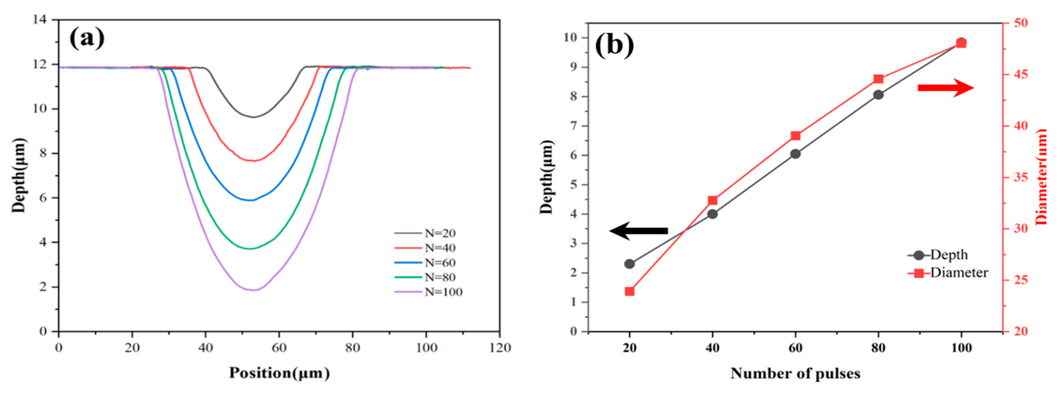
Under constant laser energy conditions, the formation of micro lens contours can be precisely regulated by varying the number of laser pulses. As depicted in
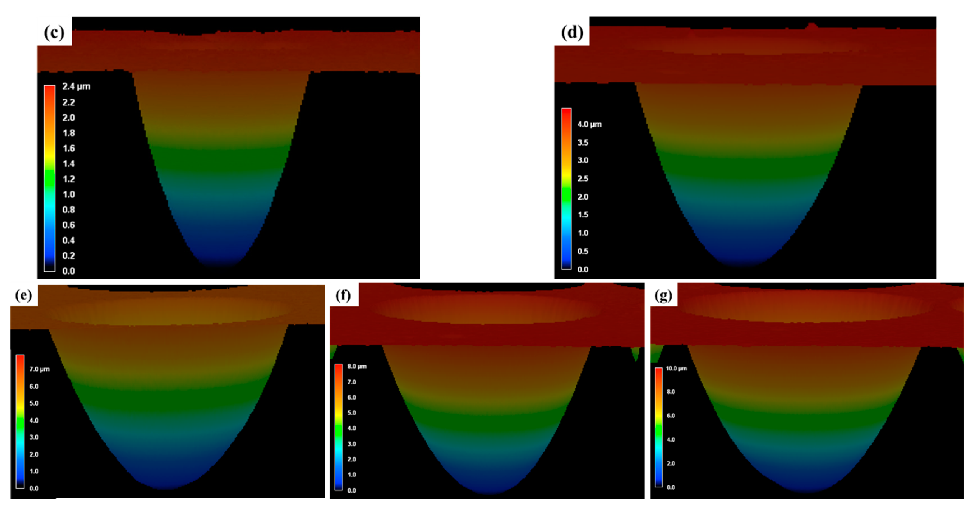
Figure 4(a), the depths of the micro lenses increase linearly with pulse numbers, measuring 2.3 μm, 4.05 μm, 6.05 μm, 8.06 μm, and 9.84 μm, respectively. Correspondingly, the diameters of the micro lens are 23.91 μm, 32.76 μm, 39.05 μm, 44.57 μm, and 48.04 μm.
Figure 4(b) illustrates a nearly linear increase in both diameter and depth of the micro lens with increasing pulse numbers. In addition, higher single pulse energies lead to increased depth and width of the micro lens profiles. This is due to the enlarging of laser processing area on the surface of fused silica, resulting in a larger etched area.
Figure 4(c)-(g) present the three-dimensional morphology of individual micro lens etched with pulse numbers ranging from 20 to 100, showcasing smooth contours and excellent surface quality for each micro lens. Notably, the surface quality of the micro lens remains consistent even with higher pulse numbers, indicating that under suitable laser parameters, adjusting the pulse number can effectively regulate the dimensions and morphology of micro lens without compromising their surface smoothness and quality.
3.4. Fabrication of Micro Lens Arrays
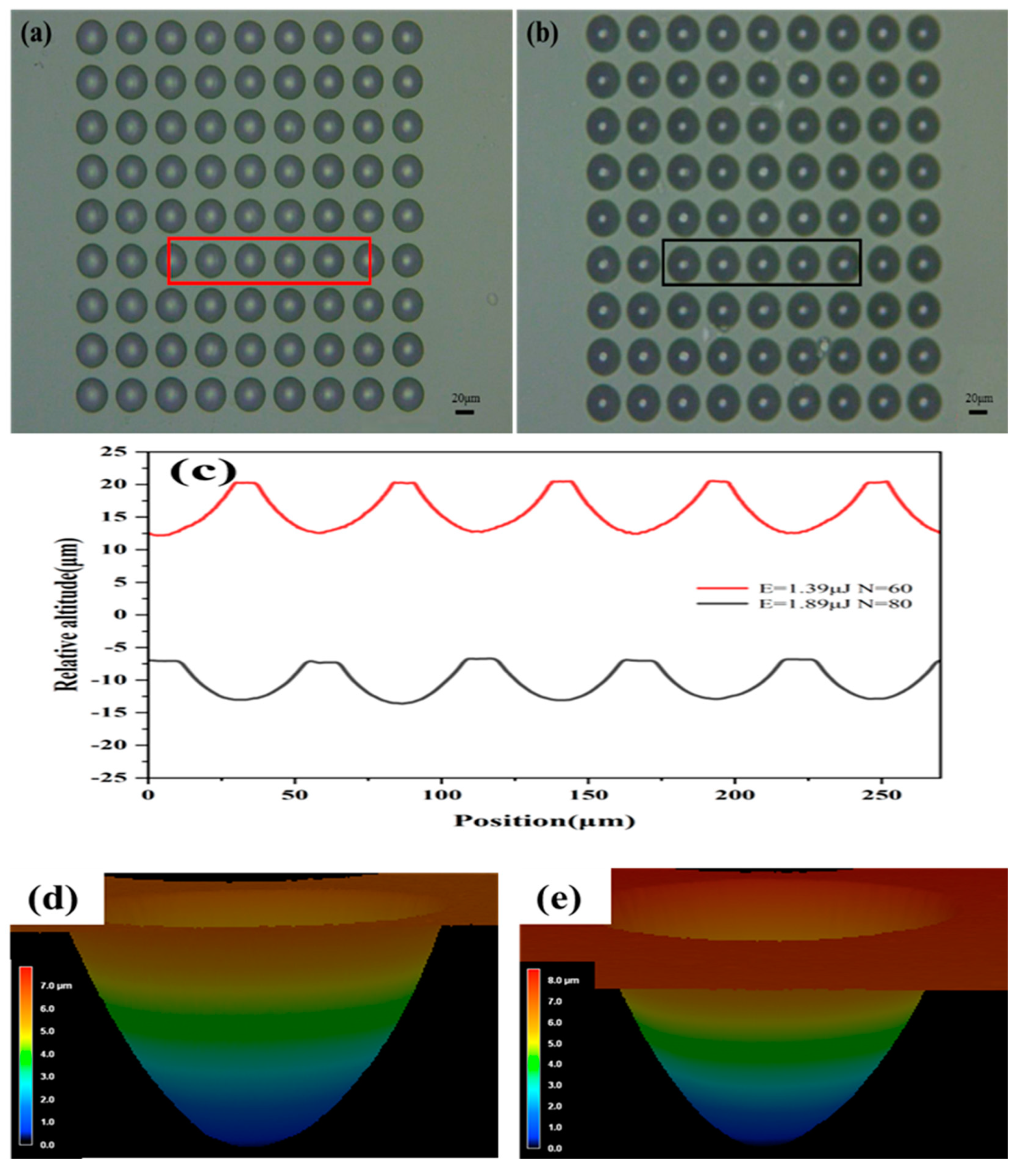
Based on the aforementioned experimental findings, we successfully produced two types of 9x9 micro lens arrays, depicted in
Figure 5 (a) and
Figure 5(b). Each MLA consists of 81 microlenses, covering an area of approximately 0.16 mm². The center to center spacing of each microlens is 50 μm. The micro lens exhibit perfectly circular and uniform surface profiles. The contour measurements of these arrays are presented in
Figure 5 (c). Among them, the red curve in
Figure 5 (c) shows the measurement result of the microlenses profiles in the solid box area of
Figure 5 (a). The results show that using a single pulse energy of 1.39 μJ and 60 pulses, the fabricated microlenses have a diameter of approximately 39.7 μm and a depth of about 19.5 μm. The average surface roughness of the microlenses concave surface is measured approximately 100 nm (each measurement area is 5 μm × 5 μm). The gray curve in
Figure 5 (c), corresponding to the measurement result within the solid box area of
Figure 5 (b), reveals that using a single pulse energy of 1.89 μJ and 80 pulses, the fabricated microlens has a diameter of about 44.2 μm and a depth of approximately 22.8 μm, with an average surface roughness of around 130 nm (each measurement area is 5 μm × 5 μm). Obviously, as the power and number of pulses increase, the depth and diameter of the implemented microlens array also increase accordingly. As we have learned from our previous process research.
Figure 5 (d) and
Figure 5(e) depict the three-dimensional morphology of a representative micro lens from each array type captured under laser scanning confocal microscopy. Both arrays demonstrate exceptional surface morphology, smoothness and uniformity. These superior characteristics are attributed to the minimal scattering observed during femtosecond laser processing and the meticulous optimization of process parameters [
27].
3.5. Imaging Performance Test
According to geometric optics, a beam of light will diverge after propagating through concave refractive microlenses, and there is no true focal point in the optical field. Nevertheless, the microlens array can still achieve imaging functionality. Because in reality, the image formed by a concave lens is a virtual image. The image plane where the virtual image is located is the intersection point of the diverging beam in the negative direction. The expressions for the focal length
f and numerical aperture (
NA) that determine the imaging performance of micro concave lenses are as follows [
28]:
where
h is the height of the microlens,
D is the diameter,
n is the refractive index of the microlens material,
f is the focal length and
NA is the Numerical aperture of microlens. The focal lengths of the micro lens arrays in
Figure 5 (a) and
Figure 5 (b) is calculated to be 43.303 μm and 48.223 μm, respectively. It is worth noting that the numerical aperture (
NA) of both MLAs are 0.458. That is to say, this study can also achieve a micro lens array with a constant aperture and variable focal length.
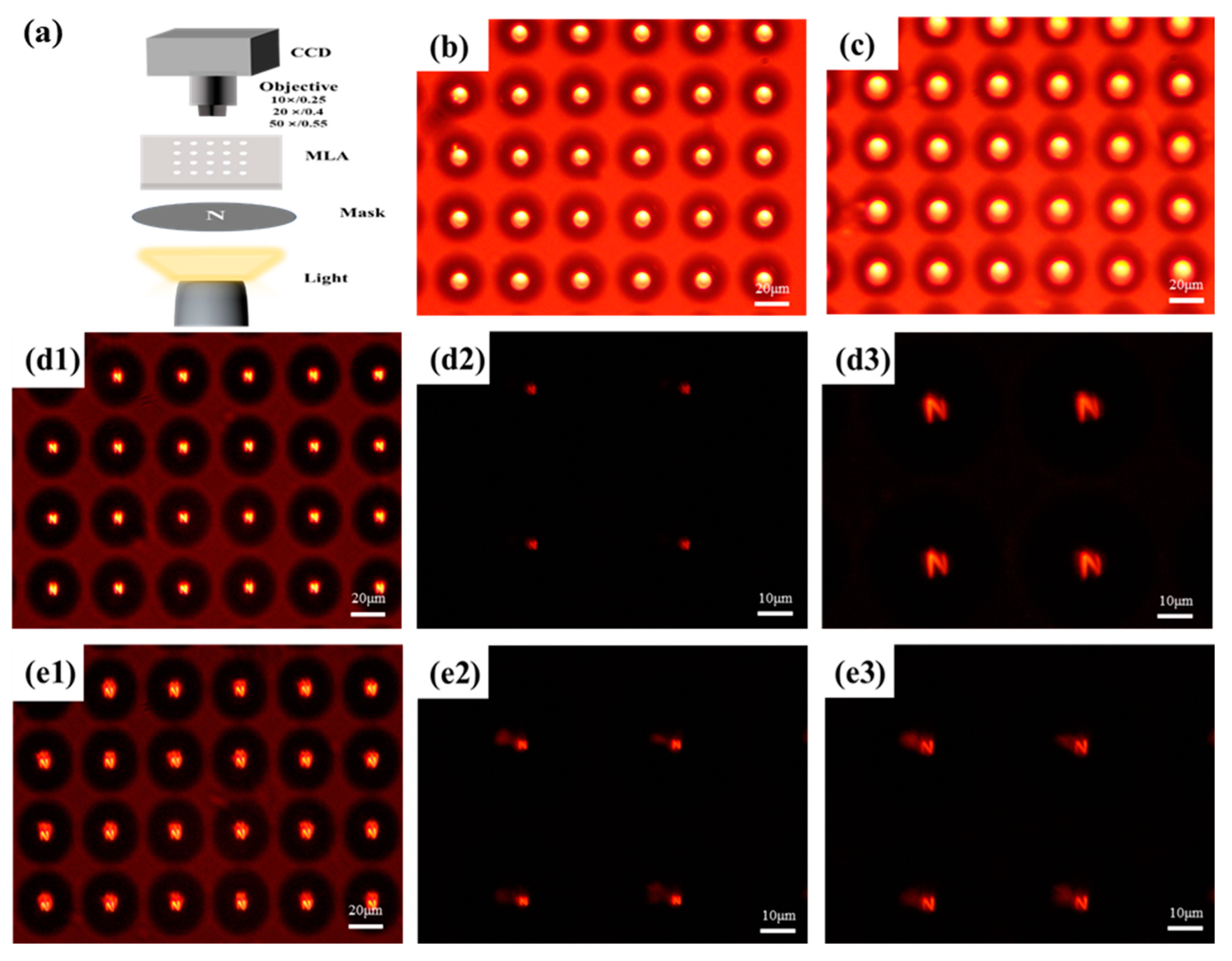
Finally, imaging performance tests were conducted with the optical setup depicted in
Figure 6(a). A halogen lamp served as the illumination source, directing light through a brown mask featuring a transparent letter ‘N’ (approximately 7 mm in size on a gray mask). The micro lens arrays fabricated focused this light onto an objective lens positioned opposite, enabling a CCD to capture bright-field and dark-field images of the letter ‘N’ on the pseudo-focal plane of the micro lens arrays.
Figure 6(b) and
Figure 6(c) present the top view of the two fabricated micro lens arrays within the imaging analysis setup. In
Figure 6(d1)-(d3) and
Figure 6(e1)-(e3), both types of micro lens arrays demonstrated clear imaging capabilities overall, with each micro lens exhibiting nearly uniform performance, indirectly indicating excellent array uniformity. Using a higher magnification 50x objective lens revealed satisfactory imaging performance of individual micro lens, as depicted in
Figure 6(d2) and
Figure 6(e2). Adjusting the relative positions of the mask and lens enabled controlled magnification of the letter ‘N’ at various magnification ratios, while maintaining clear imaging quality, as shown in
Figure 6(d3) and
Figure 6(e3). Adjusting the relative position of the mask and lens can achieve different magnifications of the letter “N” while maintaining clear imaging quality, as shown in
Figure 6 (d3) and (e3). Compared with
Figure 6 (d2), the imaging magnification of
Figure 6 (d3) has increased by about 3.0 times. In addition, the imaging magnification of
Figure 6 (e3) has increased by about 1.3 times compared to
Figure 6 (e2).
4. Conclusions
In summary, we successfully prepared multiple micro lens arrays(MLAs) on the surface of fused silica using femtosecond-laser-induced modification assisted wet etching(FLIM-EL). These microlenses exhibit excellent morphology and smooth surfaces. Firstly, step1-FLIM adopted a penetrating modified method, effectively avoiding the absorption and scattering effects of the modified layer generated by the previous pulse on the subsequent pulse, and improving the controllability of the process. Secondly, hydrofluoric acid(HF) solution was used to wet etch the modified layer completely as step2. By precisely adjusting the single pulse energy and pulse number of the laser, the size of the laser-modified regions was controlled, thereby regulating the dimensions and depths of the micro lens. Specifically, as follows:
- (1)
FLIM-EL has prepared two different types of 9x9 MLAs: pulse energy of 1.39 μ J and 60 pulses, and pulse energy of 1.89 μ J and 80 pulses. The depth of the two MLAs was 19.5 μm and 22.8 μm, and the heights was 39.7 μm and 44.2 μm, respectively. The surface roughness was as low ~100nm.
- (2)
FLIM-EL has prepared MLAs with constant numerical aperture but different focal lengths.
- (3)
The MLAs exhibits significant uniformity and excellent imaging performance, enabling clear imaging of mask patterns at adjustable magnifications (1.3X-3.0x).
The femtosecond laser assisted HF solution etching method proposed in this study effectively realizes the controllable manufacturing of fused silica MLAs. This study not only provides key technological advancements, but also emphasizes the potential in advancing the development of tunable micro-optical systems.
Author Contributions
J.W. and W.Z. conceived of the project. J.W. and W.Z. purchased equipment and built the experimental platform. K.C. did the experiment and wrote the paper. G.W. and K.Y. assisted in data testing. J.W. helped in reviewing & editing the manuscript.
Funding
This work was supported by the project National Key Research and Development Program of China (2023YFB4606701), Pioneer C Project of Chinese Academy of Sciences (XDC0150200, XDC0150201) and Special Foundation of Director of Ningbo Institute of Materials Technology & Engineering (2021SZKY0309) for the financial support.
Institutional Review Board Statement
Not applicable.
Informed Consent Statement
Not applicable.
Data Availability Statement
The data are contained within the article.
Conflicts of Interest
The authors declare no conflicts of interest.
References
- Tan, J.; Wang, G.; Li, Y.; Chen, Q. Femtosecond Laser Fabrication of Refractive/Diffractive Micro-Optical Components on Hard Brittle Materials. Laser Photon. Rev. 2023, 17, 2200692. [Google Scholar] [CrossRef]
- Li, M.; Yang, Q.; Chen, F.; Yong, J.; Biao, H.; Fang, Y.; Hou, X. Integration of Great Water Repellence and Imaging Performance on a Superhydrophobic PDMS microlens Array by Femtosecond Laser Microfabrication. Adv. Opt. Mater. 2019, 21, 1800994. [Google Scholar] [CrossRef]
- Xu, M.; Li, J.; Chang, X.; Chen, C.; Lu, H.; Wang, Z. Self-assembled microlens array with controllable curvatures for integral imaging 3D display. Opt. Lasers Eng. 2024, 180, 108322. [Google Scholar]
- Liu, F.; Bian, H.; Zhang, F.; Yang, Q.; Shan, C.; Li, M.; Ho, X.; Chen, F. IR Artificial Compound Eye. Adv. Opt. Mater. 2020, 8, 2070013. [Google Scholar] [CrossRef]
- Zhou, W.; Li, R.; Li, M.; Tao, P.; Wang, X.; Dai, S.; Song, B.; Zhang, W.; Lin, C.; Shen, X.; et al. Fabrication of microlens array on chalcogenide glass by wet etching-assisted femtosecond laser direct writing. Ceram. Int. 2022, 48, 18983–18988.
- Liu, X.; Yang, S.; Yu, L.; Chen, Q.; Zhang, Y.; Sun, H. Rapid Engraving of Artificial Compound Eyes from Curved Sapphire Substrate. Adv. Funct. Mater. 2019, 29, 1900037. [Google Scholar] [CrossRef]
- Jin, X.; Keke, W.; Jian, C.; Ping, L.; Jiahua, Z. The micro-optic photovoltaic behavior of solar cell along with microlens curved glass substrate. Energy Conv. Manag. 2015, 96, 315–321. [Google Scholar]
- Shen, X.; Wang, S.; Zhou, H.; Tuokedaerhan, K.; Chen, Y. Improving thin film solar cells performance via designing moth-eye-like nanostructure arrays. Results Phys. 2021, 20, 103713. [Google Scholar] [CrossRef]
- Jisoo, H.; Youngmin, K.; Son-gi, P.; Jong-Ho, H.; Sung-Wook, M.; Sin-Doo, L.; Byoungho, L. 3D/2D convertible projection-type integral imaging using concave half mirror array. Opt. Express 2010, 18, 20628–20637. [Google Scholar]
- Jorissen, L.; Oi, Y.; Wakunami, K.; Ichihashi, Y.; Lafruit, G.; Yamamoto, K.; Bekaert, P.; Jackin, B. Holographic Micromirror Array with Diffuse Areas for Accurate Calibration of 3D Light-Field Display. Applied Sciences 2020, 10, 7188. [Google Scholar] [CrossRef]
- K. Y.; R. A.; D. P. K.; S. A. Large area IR microlens arrays of chalcogenide glass photoresists by grayscale maskless lithography. ACS Appl. Mater. Interfaces 2013, 5, 7094–7100. [CrossRef] [PubMed]
- Liiu, J.; Liu, J.; Deng, Q.; Feng, J.; Zhou, S.; Hu, S. Intensity modulation based optical proximity optimization for the maskless lithography. Opt. Express 2020, 28, 548–557. [Google Scholar] [CrossRef]
- Zhu, X.; Fang, W.; Lei, J.; Li, Z.; Xie, F.; Cao, Y.; Zhang, Y.; Qin, F.; Li, X. Supercritical lens array in a centimeter scale patterned with maskless UV lithography. Opt. Lett. 2020, 45, 1798–1801. [Google Scholar] [CrossRef] [PubMed]
- Robert, K.; Helmut, S. Thermal reflow of polymers for innovative and smart 3D structures: A review. Mater. Sci. Semicond. Process 2018, 92, 58–72. [Google Scholar]
- Bute, M.; Dhole, S.D.; Bhoraskar, V.N.; Abhyankar, A.; Terashima, C.; Gosavi, S.; Fujishima, A. Benzophenone doped polydimethylsiloxane: Resist platform for MeV electron beam lithography assisted microlens array fabrication. Microelectron. Eng. 2021, 250, 111632. [Google Scholar] [CrossRef]
- Zhenbin, L.; Miao, X.; Hongbo, L.; Yunsheng, D. A polyvinyl alcohol microlens array with controlled curvature on discontinuous hydrophobic surface. J. Mol. Liq. 2020, 319, 114372. [Google Scholar]
- Sang, B.; Kisoo, K.; Sun, Y.; Kyung, J.; Ki, J. Multifocal microlens arrays using multilayer photolithography. Opt. Express 2020, 28, 9082–9088. [Google Scholar]
- Jin, N-H.; D-Y, Jung.; G-R, Yi.; Hyun, C. Close-packed hemispherical microlens array from two-dimensional ordered polymeric microspheres. Langmuir 2006, 22, 7358–7363. [CrossRef]
- Liu, X.; Chen, Q.; Guan, K.; Ma, Z.; Yu, Y.; Li, Q.; Tian, Z.; Sun, H. Dry-etching-assisted femtosecond laser machining. Laser Photon. Rev. 2017, 11, 1600115. [Google Scholar] [CrossRef]
- Zhu, J.; Li, Q.; Chem, Q.; Liu, B.; Wei, Z. Precise and smooth structure on InP fabricated by femtosecond laser direct writing-assisted wet etching. Opt. Laser Technol. 2024, 176, 110944. [Google Scholar] [CrossRef]
- Vorobyev, Y.A.; Guo, C. Direct femtosecond laser surface nano/microstructuring and its applications. Laser Photon. Rev. 2013, 7, 385–407. [Google Scholar] [CrossRef]
- Li, J.; Zhong, S.; Huang, J.; Qiu, P.; Wang, P.; Li, H.; Qin, C.; Miao, D.; Xu, S. Laser-guided anisotropic etching for precision machining of micro-engineered glass components. Int. J. Mach. Tools Manuf. 2024, 198, 104152. [Google Scholar] [CrossRef]
- Low, D.K.Y.; Xie, H.; Xiong, Z.; Lim, G.C. Femtosecond laser direct writing of embedded optical waveguides in aluminosilicate glass. Appl. Phys. A-Mater. Sci. Process 2005, 81, 1633–1638. [Google Scholar] [CrossRef]
- Bian, H.; Wei, Y.; Yang, Q.; Chen, F.; Zhang, F.; Guangqing, D.; Jiale, Y.; Xun, H. Direct fabrication of compound-eye microlens array on curved surfaces by a facile femtosecond laser enhanced wet etching process. Appl. Phys. Lett. 2016, 109, 221109. [Google Scholar] [CrossRef]
- Hu, Y.; Rao, S.; Wu, S.; Wei, P.; Qiu, W.; Wu, D.; Xu, B.; Ni, J.; Yang, L.; Li, J.; et al. All-Glass 3D Optofluidic Microchip with Built-in Tunable microlens Fabricated by Femtosecond Laser-Assisted Etching. Adv. Opt. Mater. 2018, 6, 1701299. [Google Scholar] [CrossRef]
- David, B.; Nathan, H. Multiscale lens design. Opt. Express 2009, 17, 10659–10674. [Google Scholar]
- Deng, H.; Qi, D.; Wang, X.; Liu, Y.; Shangguan, S.; Zhang, J.; Shen, X.; Liu, X.; Wang, J.; Zheng, H. Femtosecond laser writing of infrared microlens arrays on chalcogenide glass. Opt. Laser Technol. 2023, 159, 108953.
- Liu, X.; Yang, S.; Yu, L.; Chen, Q.; Zhang, Y.; Sun, H. Rapid Engraving of Artificial Compound Eyes from Curved Sapphire Substrate. Adv. Funct. Mater. 2019, 29, 1900037. [Google Scholar] [CrossRef]
|
Disclaimer/Publisher’s Note: The statements, opinions and data contained in all publications are solely those of the individual author(s) and contributor(s) and not of MDPI and/or the editor(s). MDPI and/or the editor(s) disclaim responsibility for any injury to people or property resulting from any ideas, methods, instructions or products referred to in the content. |
© 2024 by the authors. Licensee MDPI, Basel, Switzerland. This article is an open access article distributed under the terms and conditions of the Creative Commons Attribution (CC BY) license (http://creativecommons.org/licenses/by/4.0/).
