Preprint
Article

Study of Physical Properties of Copper Oxide Thin Films Prepared by Spin Coating for Hole Transport Applications in Perovskite Solar Cells

Altmetrics

Downloads

192

Views

113

Comments

0

Submitted:

07 August 2024

Posted:

07 August 2024

You are already at the latest version

Alerts
Abstract
Different materials prepared by appropriate synthesis methods and applying different post syn-thesis processes could be used as hole transport layer in perovskite solar cells. In the present work annealing was employed to enhance physical properties of copper oxide (CuO) thin films fabricated via spin coating technique and the effects of annealing on their optical, morphological, electrical and structural properties were investigated. The XRD findings revealed the polycrystalline structure with large crystallite size. Optical spectra showed larger transmission beyond the visible region, reduced absorption, and a decrease in bandgap energy from 1.93 eV to 1.81 eV. The Ag phonon modes at 299.22 and 304 cm-1 shown by the Raman shift confirmed the development of the CuO pure phase. FTIR spectra showed the Cu-O stretching band at 759, 764 and 446 cm−1. SEM revealed the agglomeration of nano crystallites with large grains on the surface. The carrier type conductivity of annealed CuO thin films was determined via two-point hot probe technique. Low resistivity values were determined via four-point probe method. These findings indicate that CuO thin films may be successfully used as a companion with an n-type layer in p-n junction solar cells, and a hole transport layer in perovskite solar cells.
Keywords: 
Subject: Physical Sciences  -   Applied Physics
Preprints 114546 i001Graphical abstract.

1. Introduction

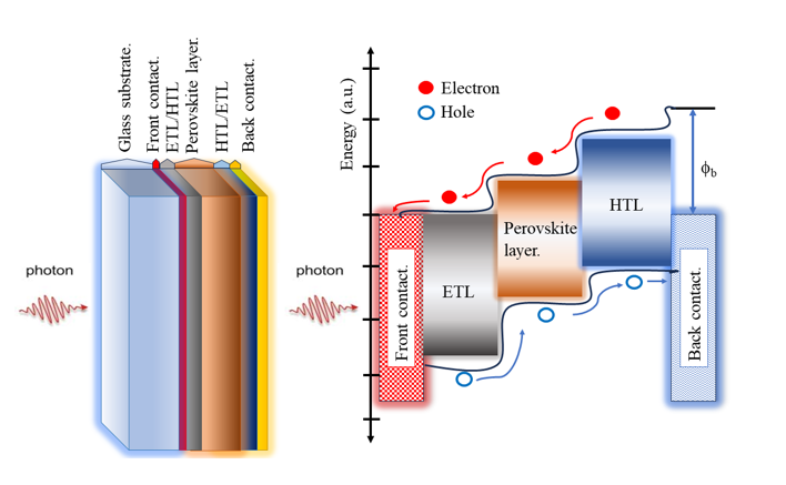
Hybrid perovskite solar cells (PSCs) having 24.6% power conversion efficiency [1] are a favourite research subject these days. Three main layers, perovskite layer electron transport layer (ETL) (Figure 1), and hole transport layer (HTL) generate and transport the charge carriers. When light falls on the perovskite layer, it generates exciton by absorbing light. Binding energy variation causes the formation of charge carriers (holes and electrons) from exciton. Holes transportation is accomplished via HTL, and electrons via ETL. At the end, holes are trapped by the back contact layer and electrons by front contact layer of transparent conducting oxides. Therefore, these layers play a crucial role in increasing the efficiency of PSCs. Charge extraction and injection rely on these layers. These layers should have the best values of energy levels to lower loss of charge and enhance charge transportation for PSCs [2,3]. Recently, many semiconductor materials like NiO, CoO, CuI, WOx, VOx, and CuO, etc, are being evaluated for use in perovskite solar cells as hole transport material [4]. But copper oxide (CuO) is the most versatile [5] and has many potential applications in photocatalysis, antibacterial activities [6], ultraviolet sensing [7], supercapacitors, displays [8], thin-film lithium-ion batteries and solar cells [9], due to its optimal band gap, high melting points, non-toxicity and high surface area. Due to its ideal bandgap energy of 1.21–2.1eV [10], CuO have a remarkable absorption coefficient (>105 cm-1). All these properties make it suitable for making hole transport layer in application of perovskite solar cells.
Several techniques are in practice for the coatings of CuO thin films [11], such as molecular beam-epitaxy [12], reactive sputtering [13], dip coating [14], magnetron sputtering [15], chemical-bath deposition [16], electro-deposition [17], co-precipitation [18], spray-coating [10], Flame hydrolysis deposition [19], pulsed laser deposition [20], and spin coating [21] etc. But spin coating is a straightforward, economically sound, and well-known coating method. Spin coating technique includes the steps; (i) mixing and stirring of the chemicals to prepare a precursor solution, (ii) allowing the solution to age and turn into a gel, (iii) coating the gel on a substrate, and (iv) annealing the thin films [22]. Various methods are used to enhance physical properties of hole transport layers [23,24]. The characteristics of films are enhanced by a number of parameters, such as doping, concentration, spinning time, chelating agents, substrate temperature, post-heating temperatures, annealing time, and spinning speed. Optimizing ageing duration and heat-treatment play a crucial role in fabricating thin films via managing optical band gaps [25] among other aspects, to produce high-quality thin films.
The physical properties of copper oxide (CuO) deposited on glass slides can be improved [26] through annealing because annealing alters the crystallite size, surface roughness, phase purity, electrical, optical, and morphological characteristics of synthesized films [27]. In this work, CuO thin films are fabricated on glass slides, and annealed at various temperatures [28] to investigate how the annealing effects can enhance the physical properties of thin films.

2. Materials and Methods

2.1. Chemicals Used in Experimental Work

Copper acetate monohydrate (Cu(C2H3O2)2.H2O, 99.999% purity), a source material with CAS No. 6046-93-1, was acquired from Sigma Aldrich and used exactly as purchased to create CuO thin films. The liquid 2-aminoethanol (CAS 141-43-5:NH2CH2CH2OH with purity >99.5%), and a reagent known as (MEA) were used as a solvent and stabiliser respectively. Microscope glass slides (CAT 7101, 1mm-1.2 mm thick) were used as substrates.

2.2. Substrates’ Cleaning

Glass slide substrates were thoroughly cleaned before depositing CuO material. This process involved three steps, (i) the glass slides were first meticulously cleaned with surfactant for 20 minutes, (ii) in the second step they were scrubbed with an electric tooth brush and soap in distilled water. (iii) In the last step, the glass slides were treated ultrasonically for 10 minutes each in IPA.

2.3. Preparation of CuO Thin Films

First, copper (II) acetate was dissolved in 100 ml of 2-methoxyethanol (C3H8O2) to prepare the precursor solution, and kept on stirring at for one hour. When the mixture became uniform, monoethanolamine (NH2CH2CH2OH, >99.5% purity) was added drop by drop during stirring process. Finally, the prepared mixture (sol-gel solution) was applied to the glass substrate via dropper placed on holder of spin coater and spun the coater at 2000 rpm for 30 s. After completing this coating process, a hot plate was used for drying at 150°C for 5 minutes before deposition of second layer. In this way five successive layers were deposited on each other. The deposited thin films ware annealed at various temperatures between 200 °C to 400 °C in the furnace for half an hour to allow the formation of well crystalline structure.

2.4. Characterizations

CuO thin films fabricated were characterized to investigate the electrical, optical, and structural properties. The mass difference method was used to calculate the thickness of the deposited thin films. The structural characteristics of all CuO thin films were determined with CuKα radiation (λ=1.5406Å) via X-ray diffractometer (BRUKER Germany), and SEM. Raman spectroscopy was used to reveal the CuO phase. To investigate optical properties a UV spectrophotometer, and FTIR were used. The hot probe method and four-point probe method were used to determine the conductivity type of prepared thin films and resistivity of thin films respectively.

3. Results and Discussion

3.1. Thin Film Thickness Measurement

Thin film thickness was estimated via simple, low coat and accurate mass difference technique [29,30,31]. The determination of mass difference of thin films and substrates involved two steps. First the mass of substrates was measured by using digital balance. and then after coating the CuO material on the substrates. The mass difference of the thin film deposited on the substrate was denoted by “ m ”. The CuO density and dimensions of the glass slides were specified as 0.006 g/mm3 [32] and 76.2 x 25.4 x1.2 mm3, respectively. Then average thickness was estimated as 189,180,175, and 176 nm by using the following equation.
t = m ρ × A
where t, Δm, ρ, and A are thickness, mass of thin film, density and area respectively.

3.2. XRD

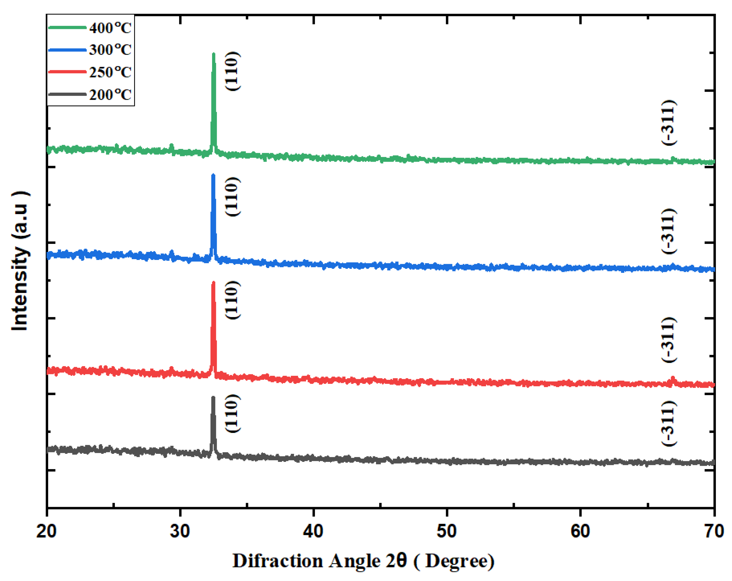
XRD patterns were obtained via Cu Kα radiations (λ=1.54 Å) for diffraction angles ranging from 20–70°. XRD spectra of a CuO thin films revealed the polycrystalline nature of prepared CuO thin films. Figure 2 shows that two prominent peaks (JCPDS card No. 01-089-2529) are present at diffraction angle (2θ) 32.17°, and 66.47° for CuO thin films orientated along (110), and (-311) planes respectively. The absence of metallic copper (Cu) and any other impurity phases in the spectra confirmed the successful preparation of the CuO thin films prepared at different annealing temperatures.
The obtained XRD data of CuO thin films is used to dislocation density, crystallite size, and microstrain. We calculated the crystallite size via Debye-Sherrers relation [33,34].
D = k λ β c o s θ
where “k”, “λ”, “β”, and “θ” were shape factor, wavelength of the incident copper Kα-radiations, FWHM, and diffraction angle respectively. The Williamson and Smallman’s formula [35] was used to calculate the dislocation density [36].
δ = n / D 2
In above equation the value of “n”, was defined as unity. The microstrain within the CuO thin films was computed utilizing following equation [37].
ε = β c o s θ / 4
where the scattering angle and FWHM were by “θ” and”β” respectively. The following equation was used to compute interplanar spacing [38].
d = n λ / 2 s i n θ
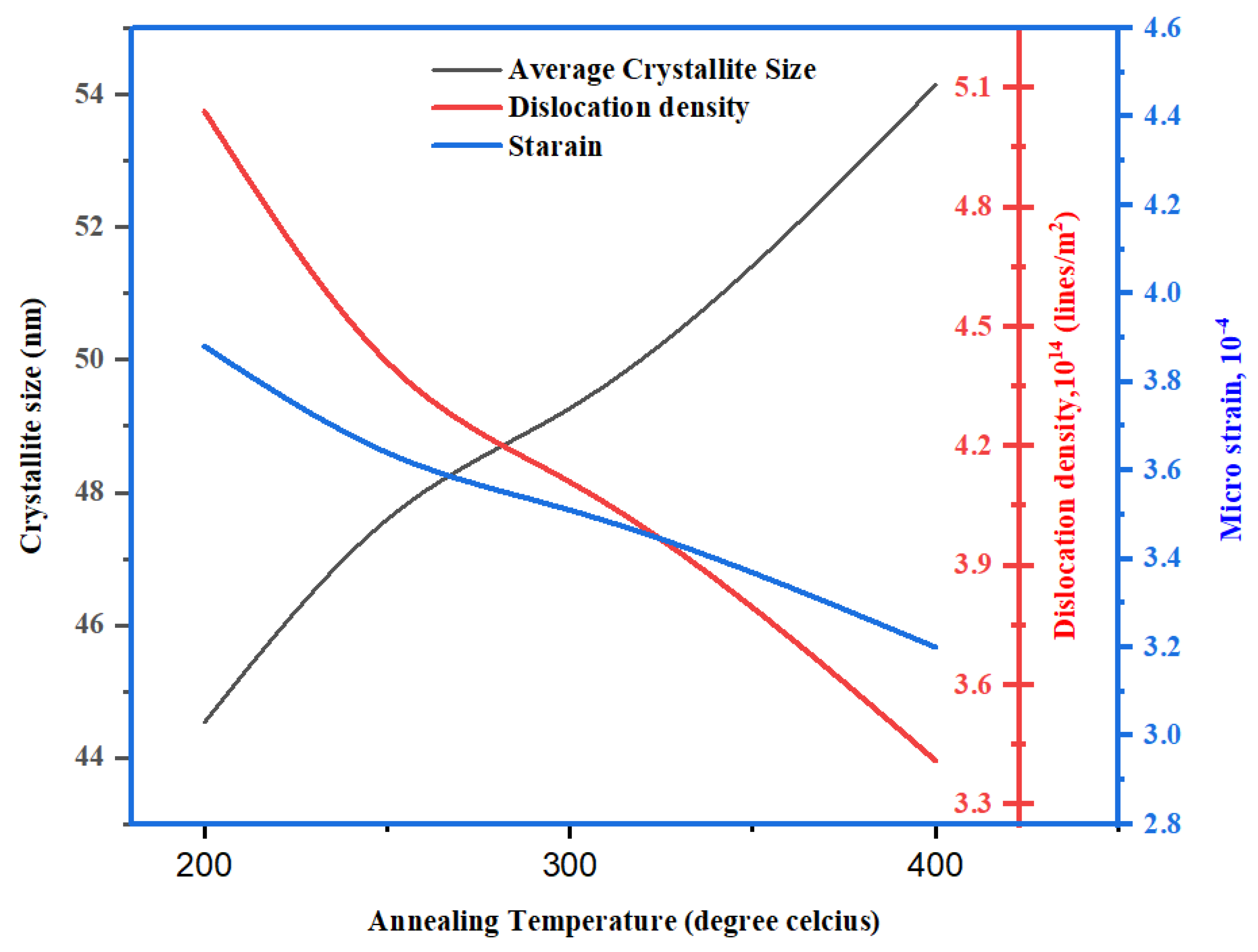
The calculated data for each of these structural parameters along a comparison with literature is provided in Table 1. A plot of how structural parameters change with annealing temperature is presented in Figure 3.
Figure 3 reveals that the average crystallite size increases [9] with annealing temperature, whereas dislocation density and micro strain decrease. A large crystallite size of 54.14 nm is observed at 400 °C which is not surprising at this annealing temperature using spin coating technique. The increase in crystallite size may be attributed to process of sintering [41]. The finding of large crystalline size range between 44.54 nm to 54.14 nm using spin coating technique is in good agreement with the literature [42]. The decrease in dislocation density and strain affects the quality and number of defects in thin films. The decrease in micro strain and dislocation density indicates less imperfections, showing good quality of the CuO thin films. Normally, large crystallite sizes are preferred in the fabrication of solar cells [45], which is found in this work. So, well-annealed CuO thin films prepared in this work have the potential to be used as a hole transport layer in perovskite solar cells.

3.3. Raman Spectra

The phase purity of CuO thin films was investigated via Raman spectroscopy. CuO coatings exhibits 12 phonon modes with C h 2 symmetry due to four primordial cell atoms [43] as explained in the following equation.
r v i b = A g + 2 B g + 4 A u + 5 B u
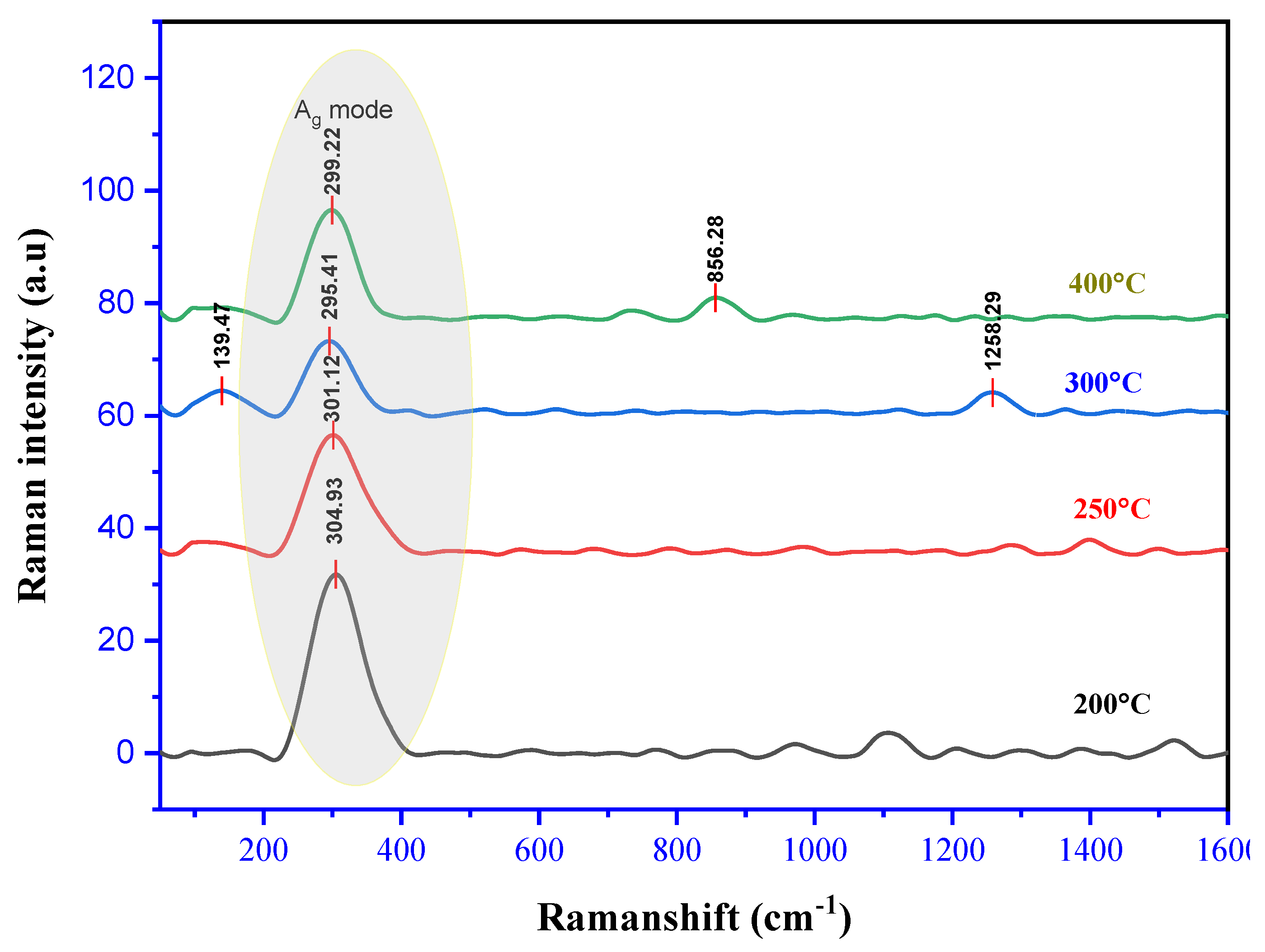
The most prevalent modes of CuO include, six infrared active modes (3Au and 3Bu), and three Raman active modes (1Ag and 2Bg). Figure 4 shows that the Raman scattering revealed the mixed Raman active modes in deposited thin films. These patterns showed a strong peak of pure CuO phase with Ag as the dominant mode which supported the XRD findings.
Figure 4 shows Raman primary phonon modes of Ag at 304.93, 301.12, 295.41, and 299.22 cm-1 are present, which are well consistent with literature and are given in Table 2.

3.4. Ultra Violet – Visible Spectroscopy

Transmission data of CuO films was acquired in the 330 to 800 nm wavelength range via UV-visible spectroscopy. The obtained transmission data was then used to calculate key optical terms such as absorption coefficient and bandgap energy [46].

3.4.1. Transmission Spectra

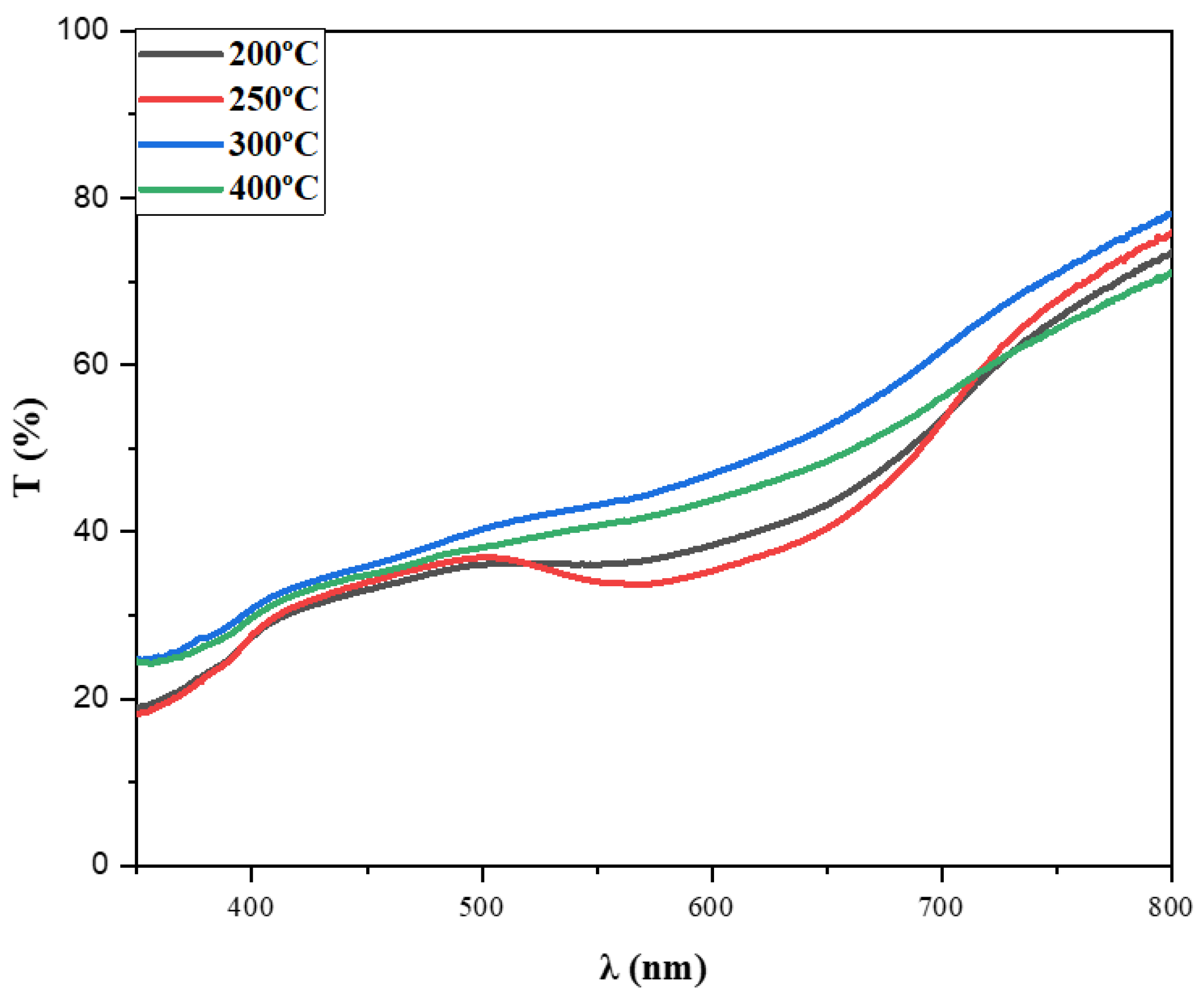
Figure 5 shows that transmission increases from 33% to 43% in the visible region at 650 nm as the annealing temperature increases up to 400 oC. This increase in transmission may be attributed to the increase in crystallite size, which reduces light scattering from grain boundaries. The increasing trend of transmission in the NIR (Near-Infrared) region consistently aligns with the literature [47]. A prominent decrease in transmission, known as the fundamental absorption band edge of CuO, occurs around 406 nm, 407 nm, and 377 nm for nanoparticles of thin films annealed at 200 °C, 250 °C, 300 °C, and 411 nm for those annealed at 400°C, respectively. The shift of the absorption edge to a higher wavelength during annealing indicates that the predicted optical band gap values will decrease as the annealing temperature increases from 200 to 400 °C, and the films are of good quality. This enhancement is related to the improvement of the crystalline microstructure, resulting in less dispersion and fewer defects. Therefore, these less dispersive CuO films can be used in perovskite solar cells as HTLs.

3.4.2. Absorption Coefficient

It is the parameter that quantifies the extent of light absorption by a specific material having certain thickness. The absorption coefficient was determined using the a specific relation (equation 7) [48].
α = 1 t .   l n T
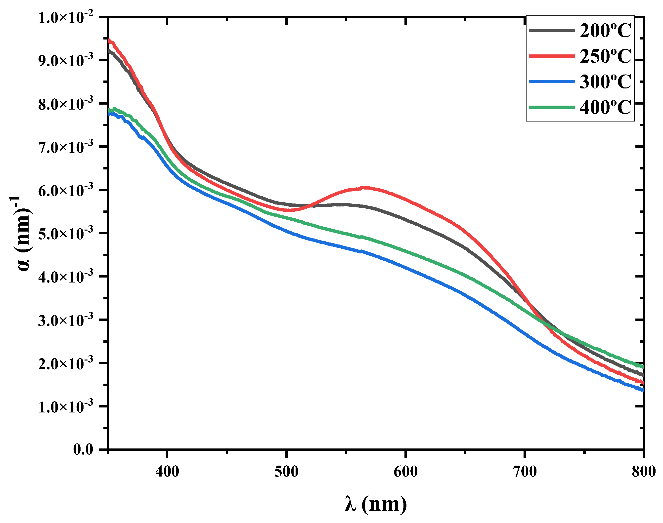
where “T” denotes the percentage of transmission and “t” thickness. Figure 6 shows a decrease in the absorption coefficient with decrease in incident light energy.
Various materials absorb light differently across different energy ranges. Figure 6 shows that absorption coefficient decreases with increasing annealing temperature in the visible region. The variation of the absorption coefficient with the annealing temperature indicates its strong dependence on annealing. In this study, energy-dependent absorption coefficients are found to be higher in the visible light energy spectrum indicating high absorption quality. These patterns are consistent with previous finding [49]. To use CuO as a hole-transporting layer, it is critical to reduce optical absorption [50] which is found in this work. So, these well annealed CuO thin films presents themselves as a good candidate to be used in laser and solar cells.

3.4.3. Bandgap

The bandgap signifies the specific amount energy required for involvement of an electron in conduction process. The bandgap (Eg) of CuO thin films was calculated via Tauc’s relation [51]. The bandgap is directly associated to the absorption coefficient (equation 8).
α h v 1 n = β h v E g
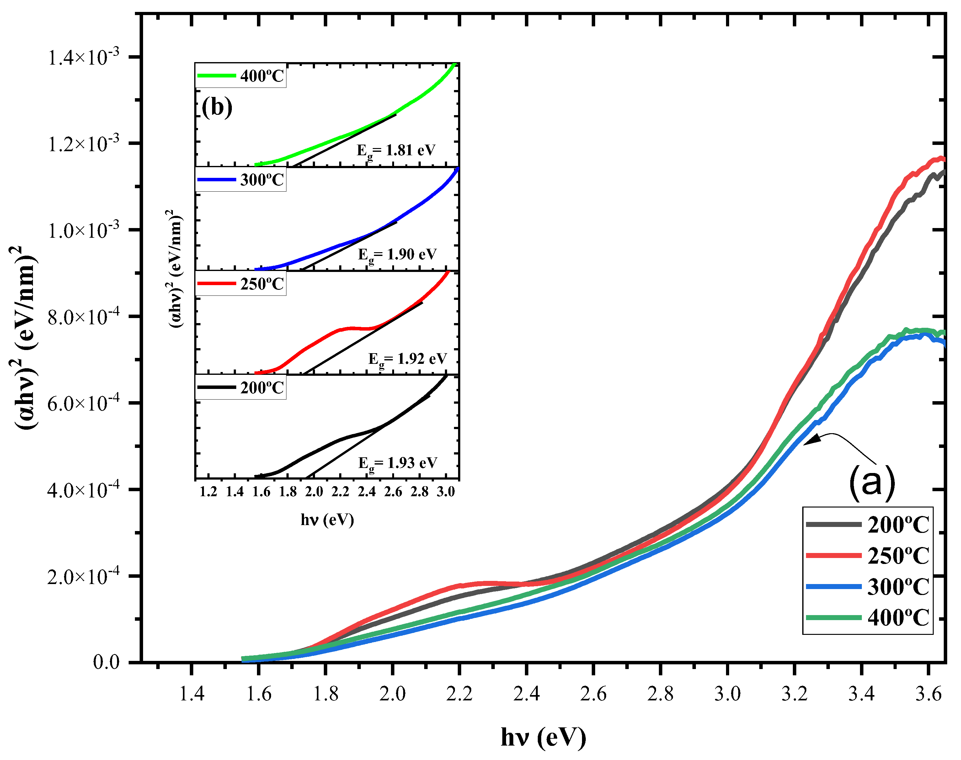
where symbol “ β ” is a constant indicates band tailing, and “ E g ” represents the optical bandgap. The exponent “n” often takes values such as 1/2, 3/2, 5/2, 7/2 or 2, 3, 4, 5, 6, corresponding to direct bandgap and indirect bandgap transitions. Figure 7 (a) presents plot of α h v 2 versus incident light “ h v ” and shows a linear segment beyond the absorption edge, aiding to identify the sample’s nature, whether indirect or direct. A linear trend is observed after the absorption edge for n = 1/2, as exhibited in Figure 7 (b) inset. Tauc’s relation (equation 9) is used to investigate the band gap energy.
α h v 2 = β h v E g
Figure 7 (a, b) illustrates the calculation of the bandgap, showing a decrease in the bandgap from1.93 eV to 1.81 eV with the increase in annealing temperature. The decrease of the bandgap may be attributed to increase in the crystallite size [43]. The principal contribution in reduction of band gap energy may also be due to a temperature dependent interaction between electrons and the lattice, which shifts the relative locations of the conduction and valence bands at higher temperature, resulting in decrease of band gap [52]. All these findings are well consistent with literature [47,51] and are compared in Table 3. These findings showed that annealing can optimize the band gap of CuO thin films to for their applications in solar cells.

3.5. FTIR Spectra

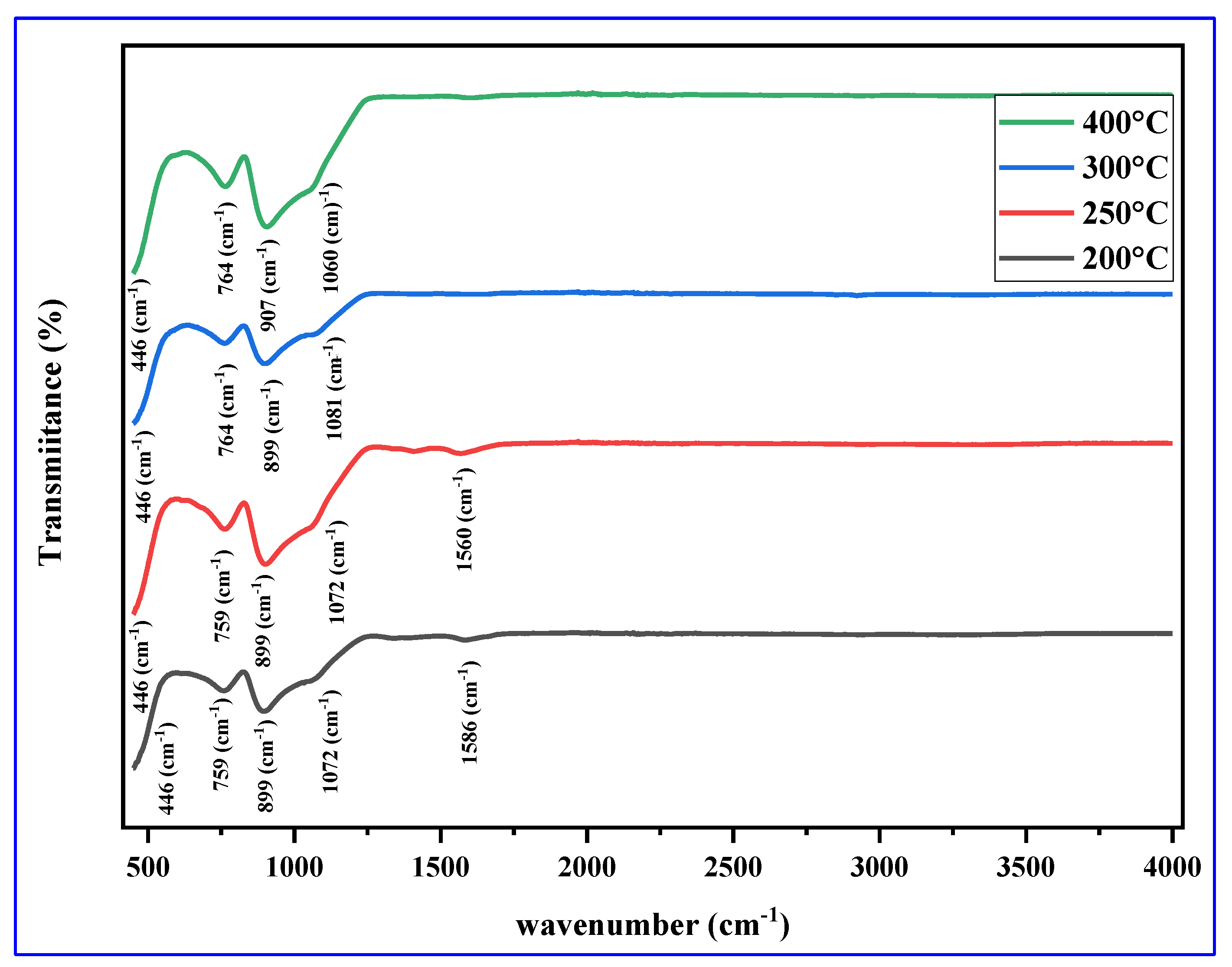
The investigation of microstructural changes in response to processing parameters, such as concentration, annealing time, annealing temperature is an important application of Fourier-transform infra-red spectroscopy [59]. Under standard conditions, Fourier-transform infra-red spectra ranging from 400 to 4000 cm-1 were collected to confirm the Cu-O bond in thin films. Cu-O stretching was observed at 759,764 and 446 cm−1 [60,61,62], band at 1586 cm−1 is associated to O-H stretching, band at 1086 cm−1 shows C-O bond bending [63] whereas, band at 910 cm−1 is associated to C-H bond [64]. Figure 8 shows the FTIR patterns of CuO thin films annealed at different temperatures range from 200 °C to 400 °C, all the absorption peaks closely match with literature presented in Table 4. It is observed that O-H vibrations are significant for thin films annealed at 200 °C then their intensity decreases at 250 °C, and are completely vanished for thin films annealed at 300 °C and 400 °C. Therefore, annealing renders CuO thin films O-H free, making these thin films better suited to be used as hole transport layers in perovskite solar cells.

3.6. Surface Morphology

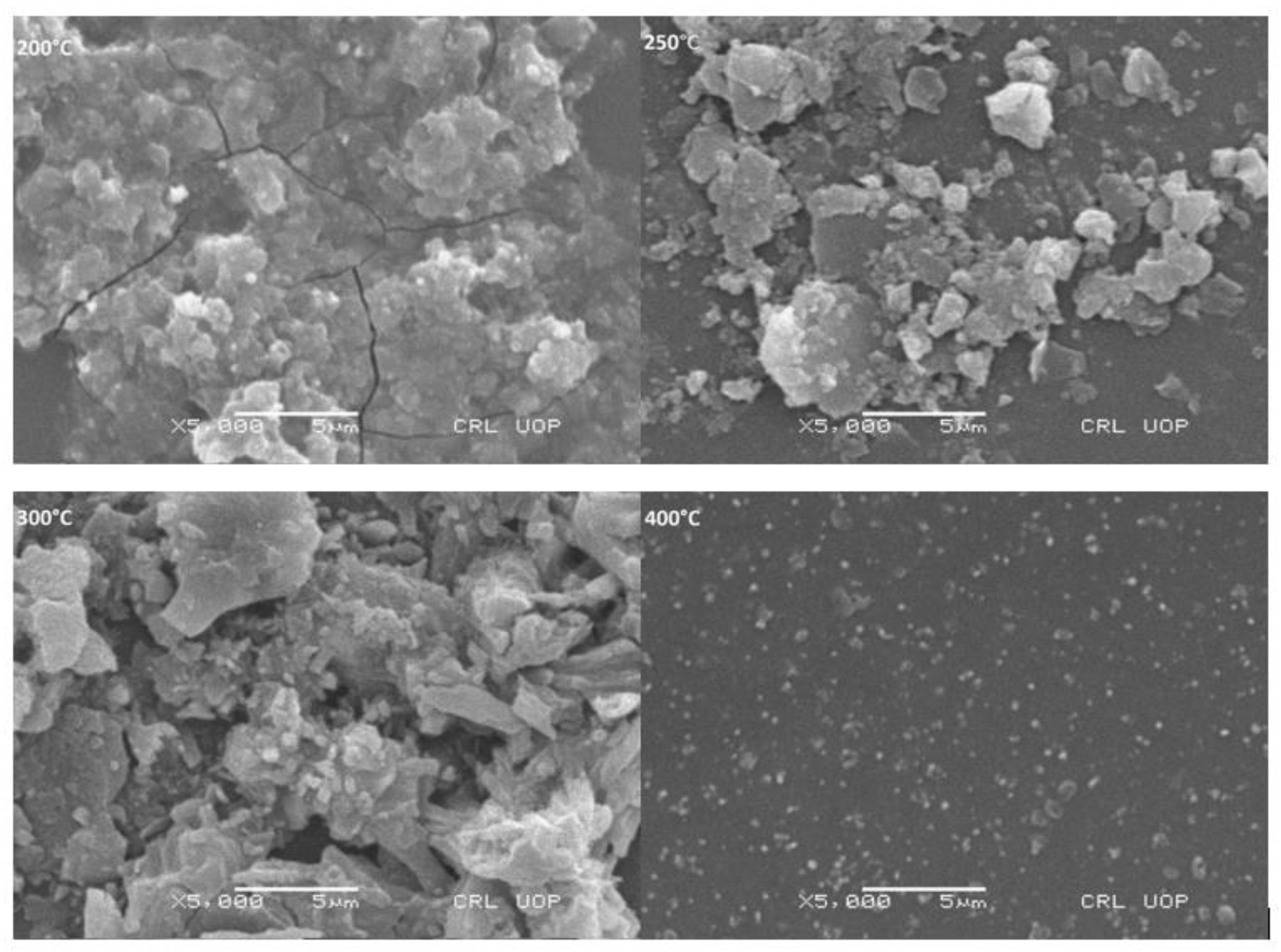
Figure 9 shows SEM images of CuO thin films annealed at different temperatures to diagnose their surface morphology. The surface features are validated upon closer study at a magnification of 5000. These SEM images show clustering of particles during first phase of nucleation, confirming the presence of agglomeration. The SEM pattern of thin film annealed at 200°C shows an uneven distribution of clustered grains over the surficial layer with cracks, amorphous granular morphology, and spherical-shaped grains. All the cracks and agglomeration may be attributed to inadequate reactions during deposition controlled by surface diffusion [69]. These surface defects can be reduced by controlling synthesis conditions such as stirring time, spinning speed or drying time because cracks normally occurred due to inappropriate synthesis conditions [70]. Whereas, SEM image of CuO thin film annealed at 250 °C reveals crack free surface, less voids spread and more even distribution compared to the thin film prepared at 200°C annealing temperature. Small spherical grains with no obvious flaws indicate complete chemical reaction occurred over the substrate surface and mixture has been thoroughly converted to CuO. Thin film prepared at 300 °C shows even more better flower shape agglomeration of nanoparticles with no cracks, Lastly, prepared CuO thin film, annealed at 400 °C shows no proper visible agglomeration indicating less featured morphology. It may be due to decomposition of clusters due to high temperature effect. These results encourage the use of crack-free CuO thin films in perovskite solar cells as a hole transport layer.

3.7. Electrical Properties

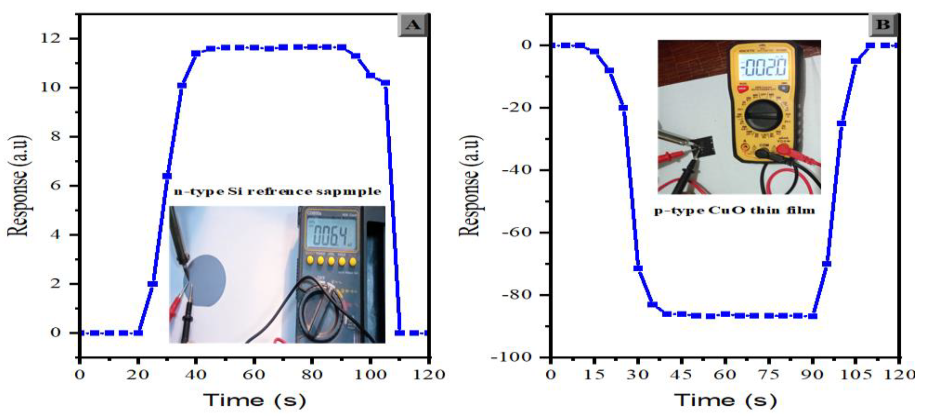
Several techniques can be used for conductivity type determination which includes [71], thermal electromotive force, wafer flat detection, rectification, the hot probe technique, and the Hall effect [31]. The hot probe technique is a simple, accurate, and low-cost method to determine the type of charge carriers [72]. In this technique, two probes are positioned at two different points on the surface of a sample under test. At first, one of the probes (anode) is heated thermally, and the majority carriers begin to diffuse from the anode (heated probe) to the cathode (cold probe) while the holes move in opposite direction. This movement of majority carriers establishes a potential gradient between the two probes. A parallel connected voltmeter senses the potential difference and indicate positive readings until heat is successively is supplied if the sample under test is of n-type material, while the panel shows negative readings when the thin film under test is of p-type [73]. We noticed positively increasing readings and plotted their response curve (Figure 10 A) which goes on increasing during heat supplied and then gradually decreases when cooled for reference silicon wafer, whereas opposite behaviour (Figure 10 B) is observed for CuO thin film. Figure 10 (B) exhibits a positive response for a silicon wafer (006.4), indicating negative conductivity. The positive response confirmed that reference Si wafer had n-type conductivity with electrons as majority charge carriers [74]. We noticed negative readings and plotted (Figure 10 B) their response curve. The opposite response is shown by CuO thin films, which goes on negative side first when heat is supplied successively and then is shifted on opposite side when cooled. A negative response on panel (-002.0) confirmed p-type conductivity of CuO thin films and same response observed for all other samples which were annealed at various annealing temperatures, indicating the presence of holes as majority charge carriers in thin films. Therefore, it is confirmed that prepared samples of CuO thin films are p-type materials and can be used for HTL application in perovskite solar cells.
The electrical resistivity of the CuO thin films was measured in air via 4-point probe technique [75]. A current was passed through the two outer probes, and the voltage was measured across the two inner probes. The sheet resistance ( R ), resistivity ( ρ ), and conductivity ( σ ) were then calculated using the equations [22].
R = π l n 2 · V I
ρ = R . t · k
σ = 1 ρ
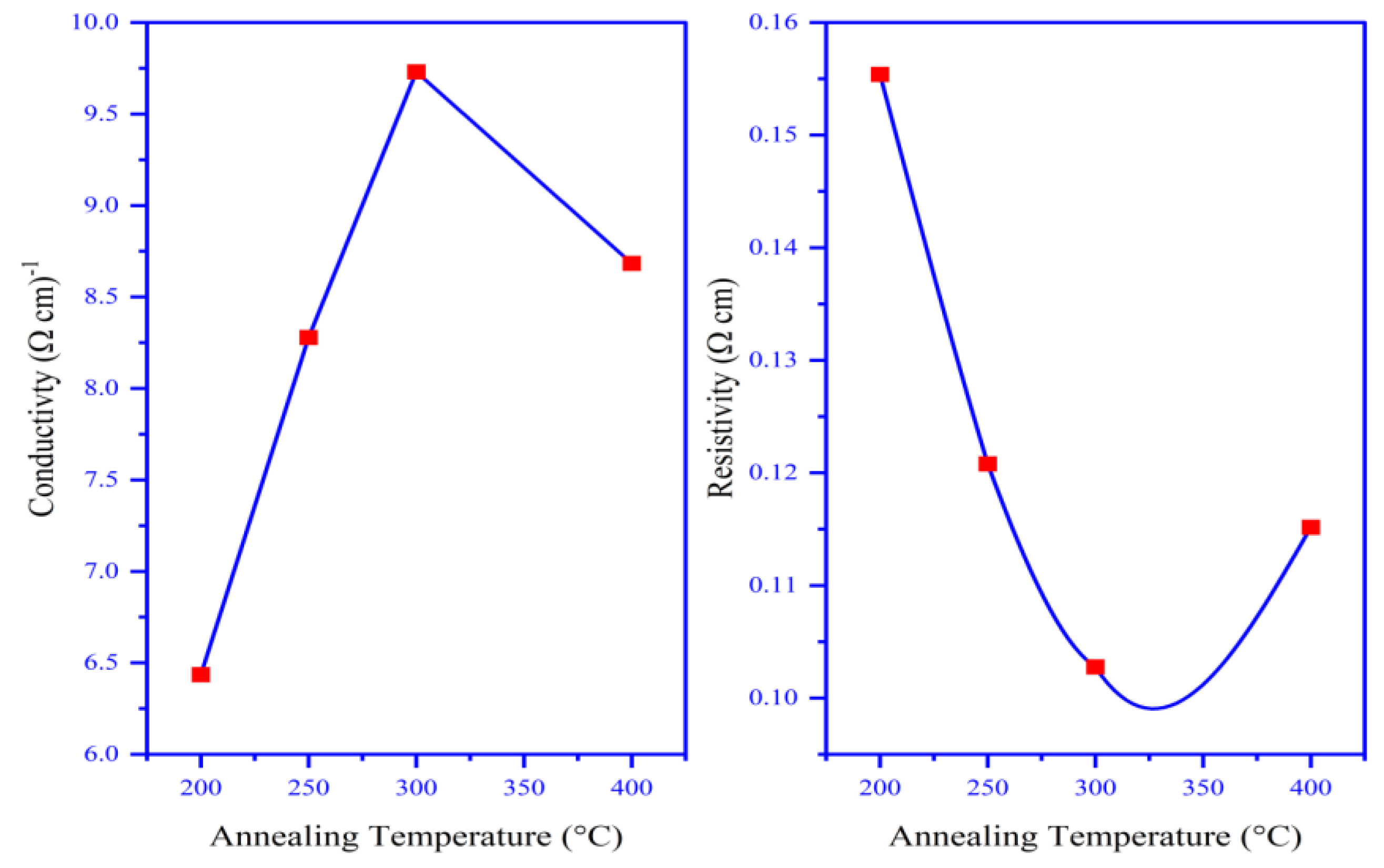
where “t” denotes thickness and “k” is the correction factor applied according to the ratio of thickness and distance between probes. Figure 11 shows the results for resistivity and conductivity. CuO is a p-type semiconductor, therefore its conductivity depends on the holes in the valence band formed by copper vacancies in the lattice structure. The increased conductivity values at 250 °C, and 300 °C may be attributed to an increase in crystallite size, which reduces grain boundaries for holes [76]. The least resistivity found (10.28x10⁻³Ω.cm) at 300 °C shows an increase in vacancies. This suggests that increasing the annealing temperature can enhance the carrier mobility and electrical conductivity. The findings presented in Table 5 are in line with previous research [27,53,77]. Therefore, CuO thin films with low resistivity characteristic and p-type carriers (holes) have potential for perovskite solar cell applications.

5. Conclusions

This work used a spin coating deposition approach for the fabrication of CuO thin films on glass slides to enhance. Then these thin films were annealed at various temperatures (200, 250, 300 and 400 °C) in order to enhance their properties. XRD revealed a large crystallite size of the order 44.54 nm, increasing with higher annealing temperatures up to 400 °C. Raman spectra validated the Ag phase as a pure dominant phase. The band gap energy values for thin films annealed at different temperatures (200, 250, 300, and 400 °C) are 1.93, 1.92, 1.90 and 1.81 eV, respectively. Optical characterization also indicated that the band gap of the samples decreased with the increase in annealing temperature. The optical investigations revealed the temperature-dependent variations in transmittance, absorption coefficient, and optical band gap. Hot probe technique confirmed that all fabricated CuO thin films demonstrated the p-type conductivity, and showed low resistivity, which is required for application as a hole transport layer in perovskite solar cells. We can conclude that annealing can enhance the structural, optical, and electrical properties of CuO thin films in terms of large crystallite size, reduced optical absorption, optimised band gap, and low resistivity making them a good candidate for their use in perovskite solar cells as hole transport layers.

Author Contributions

Conceptualization, Ghulam Hasnain Tariq, Muhammad Imran and Muhammad Abbas; Methodology, Ghulam Hasnain Tariq and Muhammad Abbas; Formal analysis, Ghulam Hasnain Tariq and Muhammad Abbas, Muhammad Haseeb-u-Rehman; Investigation, Ghulam Hasnain Tariq, Muhammad Imran and Muhammad Abbas; Data curation, Ghulam Hasnain Tariq, Muhammad Imran and Muhammad Abbas; Writing—original draft preparation, Ghulam Hasnain Tariq and Muhammad Abbas; Writing—review and editing, Ghulam Hasnain Tariq, Muhammad Imran and Muhammad Abbas; Supervision, Ghulam Hasnain Tariq; Project administration, Ghulam Hasnain Tariq; Funding acquisition, Ghulam Hasnain Tariq. All authors have read and agreed to the published version of the manuscript.

Funding

This research was funded by Higher Education Commission (HEC) Pakistan through Project No: “10304/Punjab/NRPU/R&D/HEC/2017” under National Research Program for Universities (NRPU).

Data Availability Statement

The original contributions presented in the study are included in the article, further inquiries can be directed to the corresponding author.

Acknowledgments

Authors acknowledge to Higher Education Commission (HEC) Pakistan for financial assistance through Project No: “10304/Punjab/NRPU/R&D/HEC/2017” under National Research Program for Universities (NRPU).

Conflicts of Interest

The authors declare no conflicts of interest. The funders had no role in the design of the study; in the collection, analyses, or interpretation of data; in the writing of the manuscript; or in the decision to publish the results”.

References

  1. Li, G.; Su, Z.; Canil, L.; Hughes, D.; Aldamasy, M.H.; Dagar, J.; Trofimov, S.; Wang, L.; Zuo, W.; Jerónimo-Rendon, J.J.; et al. Highly efficient p-i-n perovskite solar cells that endure temperature variations. Science 2023, 379, 399–403. [Google Scholar] [CrossRef] [PubMed]
  2. Shao, Y.; Yuan, Y.; Huang, J. Correlation of energy disorder and open-circuit voltage in hybrid perovskite solar cells. Nature Energy 2016, 1, 1–6. [Google Scholar] [CrossRef]
  3. You, J.; Meng, L.; Song, T.-B.; Guo, T.-F.; Yang, Y.M.; Chang, W.-H.; Hong, Z.; Chen, H.; Zhou, H.; Chen, Q. Improved air stability of perovskite solar cells via solution-processed metal oxide transport layers. Nature nanotechnology 2016, 11, 75–81. [Google Scholar] [CrossRef] [PubMed]
  4. Kabir, M.H.; Ibrahim, H.; Ayon, S.A.; Billah, M.M.; Neaz, S. Structural, nonlinear optical and antimicrobial properties of sol-gel derived, Fe-doped CuO thin films. Heliyon 2022, 8, e10609. [Google Scholar] [CrossRef] [PubMed]
  5. Yıldız, T.; Kati, N.; Gül, B. Characterization of CuO doped CdO nanomaterials synthesized by sol gel spin coating and hydrothermal method. Materials Science and Engineering: B 2023, 290, 116306. [Google Scholar] [CrossRef]
  6. Kumar, P.; Mathpal, M.C.; Prakash, J.; Viljoen, B.C.; Roos, W.; Swart, H. Band gap tailoring of cauliflower-shaped CuO nanostructures by Zn doping for antibacterial applications. Journal of Alloys and Compounds 2020, 832, 154968. [Google Scholar] [CrossRef]
  7. Bashir, A.; Naz, A.; Sultan, M.; Bashir, R.; Ali, N.Z.; Iqbal, A.; Akhter, Z. Influence of manganese and nickel doping on optical and electric properties of CuO nanostructures for optoelectronic applications. International Journal of Nanoparticles 2022, 14, 13–30. [Google Scholar] [CrossRef]
  8. Moumen, A.; Kumarage, G.C.; Comini, E. P-type metal oxide semiconductor thin films: Synthesis and chemical sensor applications. Sensors 2022, 22, 1359. [Google Scholar] [CrossRef]
  9. Bougharouat, A.; Touka, N.; Talbi, D.; Baddari, K. Hydrophobic Properties of CuO Thin Films Obtained by Sol-Gel Spin Coating Technique-Annealing Temperature Effect. In Proceedings of the Annales de Chimie-Science des Matériaux; 2021; pp. 439–445. [Google Scholar]
  10. Benaissa, N.; Bentour, H.; Garmim, T.; El Jouad, Z.; Louardi, A.; Hartiti, B.; Monkade, M.; El Kenz, A.; Benyoussef, A. Experimental and DFT TB-mBJ calculations studies of structural, morphological, electronic, optical and electrical properties of copper oxide thin films. Optical Materials 2023, 136, 113433. [Google Scholar] [CrossRef]
  11. Güney, H.; İskenderoğlu, D.; Güldüren, M.E.; Demi̇r, K.Ç.; Karadeniz, S.M. An investigation on CuO thin films grown by ultrasonic spray pyrolysis at different substrate temperatures: Structural, optical and supercapacitor electrode characterizations. Optical Materials 2022, 132, 112869. [Google Scholar] [CrossRef]
  12. Kim, C.K.; Drozdov, I.K.; Fujita, K.; Davis, J.S.; Božović, I.; Valla, T. In-situ angle-resolved photoemission spectroscopy of copper-oxide thin films synthesized by molecular beam epitaxy. Journal of Electron Spectroscopy and Related Phenomena 2022, 257, 146775. [Google Scholar] [CrossRef]
  13. Wisz, G.; Sawicka-Chudy, P.; Wal, A.; Potera, P.; Bester, M.; Płoch, D.; Sibiński, M.; Cholewa, M.; Ruszała, M. TiO2: ZnO/CuO thin film solar cells prepared via reactive direct-current (DC) magnetron sputtering. Applied Materials Today 2022, 29, 101673. [Google Scholar] [CrossRef]
  14. Chang, C.-J.; Lai, C.-W.; Jiang, W.-C.; Li, Y.-S.; Choi, C.; Yu, H.-C.; Chen, S.-J.; Choi, Y. Fabrication and characterization of P-type semiconducting copper oxide-based thin-film photoelectrodes for solar water splitting. Coatings 2022, 12, 1206. [Google Scholar] [CrossRef]
  15. AF Lahiji, F.; Bairagi, S.; Magnusson, R.; Sortica, M.A.; Primetzhofer, D.; Ekström, E.; Paul, B.; Le Febvrier, A.; Eklund, P. Growth and optical properties of NiO thin films deposited by pulsed dc reactive magnetron sputtering. Journal of Vacuum Science & Technology A 2023, 41, 063402. [Google Scholar] [CrossRef]
  16. Rahman, R.A.; Zulkefle, M.A.; binti Alip, R.I.; Herman, S.H. Determination of CuO Concentration for ZnO-NRs/P3HT/CuO as the Potential Thin Film in Solar Cell Application. Proceedings of 2022 IEEE International Conference on Semiconductor Electronics (ICSE); 2022; pp. 136–139. [Google Scholar] [CrossRef]
  17. Möllers, P.V.; Wei, J.; Salamon, S.; Bartsch, M.; Wende, H.; Waldeck, D.H.; Zacharias, H. Spin-Polarized Photoemission from Chiral CuO Catalyst Thin Films. ACS nano 2022, 16, 12145–12155. [Google Scholar] [CrossRef]
  18. Aftab, M.; Butt, M.; Ali, D.; Bashir, F.; Khan, T.M. Optical and electrical properties of NiO and Cu-doped NiO thin films synthesized by spray pyrolysis. Optical Materials 2021, 119, 111369. [Google Scholar] [CrossRef]
  19. Butt, M.A. Thin-film coating methods: A successful marriage of high-quality and cost-effectiveness—A brief exploration. Coatings 2022, 12, 1115. [Google Scholar] [CrossRef]
  20. Al-Dujayli, S.; Ali, N. The effects of CuO doping on structural, electrical and optical properties of CdO thin films deposited by pulsed laser deposition technique. JOURNAL OF OVONIC RESEARCH 2022, 18, 579–590. [Google Scholar] [CrossRef]
  21. Yildirimcan, S. Effect of ageing on electrical properties of Fe-doped CuO thin films deposited by spin coating technique. Indian Journal of Physics 2023, 97, 1707–1716. [Google Scholar] [CrossRef]
  22. Absike, H.; Labrim, H.; Hartiti, B.; Tahri, M.; Ez-Zahraouy, H. Influence of spinning speed on the physical properties of sol-gel spin coated CuO films. Molecular Crystals and Liquid Crystals 2020, 711, 18–31. [Google Scholar] [CrossRef]
  23. Zhang, J.; Tan, C.H.; Du, T.; Morbidoni, M.; Lin, C.-T.; Xu, S.; Durrant, J.R.; McLachlan, M.A. ZnO-PCBM bilayers as electron transport layers in low-temperature processed perovskite solar cells. Science Bulletin 2018, 63, 343–348. [Google Scholar] [CrossRef]
  24. Chen, W.; Zhou, Y.; Wang, L.; Wu, Y.; Tu, B.; Yu, B.; Liu, F.; Tam, H.W.; Wang, G.; Djurišić, A.B. Molecule-doped nickel oxide: Verified charge transfer and planar inverted mixed cation perovskite solar cell. Advanced Materials 2018, 30, 1800515. [Google Scholar] [CrossRef] [PubMed]
  25. Touka, N.; Tabli, D.; Badari, K. Effect of annealing temperature on structural and optical properties of copper oxide thin films deposited by sol-gel spin coating method. Journal of Optoelectronics and Advanced Materials 2019, 21, 698–701. [Google Scholar]
  26. Koshy, A.M.; Sudha, A.; Yadav, S.K.; Swaminathan, P. Effect of substrate temperature on the optical properties of DC magnetron sputtered copper oxide thin films. Physica B Condensed Matter 2023, 650, 414452. [Google Scholar] [CrossRef]
  27. Al Armouzi, N.; El Hallani, G.; Liba, A.; Zekraoui, M.; Hilal, H.S.; Kouider, N.; Mabrouki, M. Effect of annealing temperature on physical characteristics of CuO films deposited by sol-gel spin coating. Materials Research Express 2019, 6, 116405. [Google Scholar] [CrossRef]
  28. Kamarozaman, N.S.; Zulkefle, M.A.; Rahman, R.A.; Rosli, A.B.; Zainal, N.; Him, N.R.N.; Herman, S.H.; Zulkifli, Z. Annealing Effect on the EGFET Based pH Sensing Performance of Solgel Spin-coated CuO Thin Film. International Journal of Nanoelectronics & Materials 2022, 15. [Google Scholar]
  29. Akl, A.A.; Hassanien, A.S. Comparative microstructural studies using different methods: Effect of Cd-addition on crystallography, microstructural properties, and crystal imperfections of annealed nano-structural thin CdxZn1-xSe films. Physica B Condensed Matter 2021, 620, 413267. [Google Scholar] [CrossRef]
  30. Kul, M. Electrodeposited SnS film for photovoltaic applications. Vacuum 2014, 107, 213–218. [Google Scholar] [CrossRef]
  31. Faridi, A.W.; Imran, M.; Tariq, G.H.; Ullah, S.; Noor, S.F.; Ansar, S.; Sher, F. Synthesis and characterization of high-efficiency halide perovskite nanomaterials for light-absorbing applications. Industrial & Engineering Chemistry Research 2022, 62, 4494–4502. [Google Scholar]
  32. Chang, M.-H.; Liu, H.-S.; Tai, C.Y. Preparation of copper oxide nanoparticles and its application in nanofluid. Powder technology 2011, 207, 378–386. [Google Scholar] [CrossRef]
  33. Fath, F.N.; Ramadhanti, S.; Purwaningsih, S.Y.; Asrori, Z.; Cahyono, Y. Optical and structural properties of CuO thin film by spin coating method. AIP Conf. Proc. 2023, 2604, 020023. [Google Scholar] [CrossRef]
  34. Nesa, M.; Sharmin, M.; Bhuiyan, A. Role of Zn dopants on the surface morphology, chemical structure and DC electrical transport properties of nanostructured p-type CuO thin films. Materials Science in Semiconductor Processing 2021, 122, 105479. [Google Scholar] [CrossRef]
  35. Begum, A.; Hussain, A.; Rahman, A. Effect of deposition temperature on the structural and optical properties of chemically prepared nanocrystalline lead selenide thin films. Beilstein Journal of Nanotechnology 2012, 3, 438–443. [Google Scholar] [CrossRef] [PubMed]
  36. El Sayed, A.M.; Shaban, M.; Said, G. Characterization of Different Metal Oxides Thin Films Deposited by Spin Coating Technique. Labyrinth Fayoum Journal of Science and Interdisciplinary Studies 2023, 1, 59–66. [Google Scholar] [CrossRef]
  37. Tabli, D.; Touka, N.; Baddari, K.; Selmi, N. Pb-doped CuO thin films synthetized by sol-gel method. Advances in Materials Science 2022, 22, 5–13. [Google Scholar] [CrossRef]
  38. Jhansi, N.; Balasubramanian, D.; Raman, R.; Mohanraj, K. Influence of aluminum ion on the structural, optical, and electrical properties of CuO thin films for the PN-Junction diode application. Materials Science for Energy Technologies 2022, 5, 433–443. [Google Scholar] [CrossRef]
  39. Shehab, A.A.; Aabed, M.A.; Abd, A.N. Fabrication And Characterization Of P-Cuo/N-Si Heterojunction For Solar Cell Applications. Engg Sci Technol 2017, 4, 2458–9403. [Google Scholar]
  40. Saadaoui, F.; Rjeb, A.; Akharkhach, B.; Nfissi, A.; Sayouri, S. Effect of thickness and annealing temperature on the structural properties of CuO thin films prepared by sol-gel spin coating technique. Journal of Ceramic Processing Research 2019, 20, 139–142. [Google Scholar] [CrossRef]
  41. Sabli, N.; Talib, Z.A.; Wan Mahmood, M.Y.; Zainal, Z.; Hilal, H.S.; Husin, M.S. Effect of annealing on the properties of SnSe film prepared by thermal vacuum evaporation in the presence of argon gas. Advanced Materials Research 2014, 1024, 323–326. [Google Scholar] [CrossRef]
  42. Armouzi, N.A. Effect of annealing temperature on physical characteristics of CuO films deposited by sol-gel spin coating. Material Research Expesses 2019, 6, 116405. [Google Scholar] [CrossRef]
  43. Dhaouadi, M.; Jlassi, M.; Sta, I.; Miled, I.B.; Mousdis, G.; Kompitsas, M.; Dimassi, W. Physical properties of copper oxide thin films prepared by sol–gel spin–coating method. Am. J. Phys. Appl 2018, 6, 43–50. [Google Scholar] [CrossRef]
  44. Abouabassi, K.; Atourki, L.; Sala, A.; Ouafi, M.; Boulkaddat, L.; Ait Hssi, A.; Labchir, N.; Bouabid, K.; Almaggoussi, A.; Gilioli, E. Annealing effect on one step electrodeposited CuSbSe2 thin films. Coatings 2022, 12, 75. [Google Scholar] [CrossRef]
  45. Chand, P.; Gaur, A.; Kumar, A.; Gaur, U.K. Structural and optical study of Li doped CuO thin films on Si (1 0 0) substrate deposited by pulsed laser deposition. Applied surface science 2014, 307, 280–286. [Google Scholar] [CrossRef]
  46. Musa, A.; Farhad, S.; Gafur, M.; Jamil, A. Effects of withdrawal speed on the structural, morphological, electrical, and optical properties of CuO thin films synthesized by dip-coating for CO2 gas sensing. AIP Advances 2021, 11, 115004. [Google Scholar] [CrossRef]
  47. Bunea, R.; Saikumar, A.K.; Sundaram, K. A comparison of optical properties of CuO and Cu2O thin films for solar cell applications. Materials Sciences and Applications 2021, 12, 315–329. [Google Scholar] [CrossRef]
  48. Hossain, M.F.; Pervez, M.S.; Nahid, M. Influence of film thickness on optical and morphological properties of TiO2 thin films. Emerging Materials Research 2020, 9, 186–191. [Google Scholar] [CrossRef]
  49. Sawicka-Chudy, P.; Sibiński, M.; Wisz, G.; Rybak-Wilusz, E.; Cholewa, M. Numerical analysis and optimization of Cu2O/TiO2, CuO/TiO2, heterojunction solar cells using SCAPS. Journal of Physics: Conference Series 2018, 1033, 012002. [Google Scholar] [CrossRef]
  50. Lee, Y.S.; Heo, J.; Winkler, M.T.; Siah, S.C.; Kim, S.B.; Gordon, R.G.; Buonassisi, T. Nitrogen-doped cuprous oxide as a p-type hole-transporting layer in thin-film solar cells. Journal of Materials Chemistry A 2013, 1, 15416–15422. [Google Scholar] [CrossRef]
  51. Diachenko, O.; Kováč Jr, J.; Dobrozhan, O.; Novák, P.; Kováč, J.; Skriniarova, J.; Opanasyuk, A. Structural and optical properties of CuO thin films synthesized using spray pyrolysis method. Coatings 2021, 11, 1392. [Google Scholar] [CrossRef]
  52. Varshni, Y.P. Temperature dependence of the energy gap in semiconductors. physica 1967, 34, 149–154. [Google Scholar] [CrossRef]
  53. Hussain, A.N.; Hassoon, K.I.; Hassan, M.A. Effect of annealing on copper oxide thin films and its application in solar cells. J. Phys.: Conf. Ser. 2020; 1530, p. 012140. [Google Scholar] [CrossRef]
  54. Dahham, N.A. Annealing temperature effect on the Structure, Morphology and Optical properties of Copper Oxide CuO thin Films. Tikrit Journal of Pure Science 2018, 22, 115–124. [Google Scholar] [CrossRef]
  55. Jundale, D.; Joshi, P.; Sen, S.; Patil, V. Nanocrystalline CuO thin films: Synthesis, microstructural and optoelectronic properties. Journal of Materials Science Materials in Electronics 2012, 23, 1492–1499. [Google Scholar] [CrossRef]
  56. Kabir, M.H.; Ibrahim, H.; Billah, M.M. Effect of stabilizer on sol ageing for CuO thin films synthesized by sol-gel spin coating. AIP Conf. Proc. 2021, 2324, 030007. [Google Scholar] [CrossRef]
  57. Cahyono, Y.; Ramadhanti, S.; Fatimah, S.; Dewi, Y.; Asrori, M. Structure and optical properties study of annealed CuO films for development of perovskite-based solar cells. Proceedings of Journal of Physics: Conference Series; p. 012061.
  58. Sharma, M.S.D.a.S.K. Structural, morphological and optical studies of nanocrystalline CuO thin films by solution processed Spin Coating technique. Journal of Emerging Technologies and Innovative Research 2019, 6, 669–674. [Google Scholar] [CrossRef]
  59. Innocenzi, P. Infrared spectroscopy of sol–gel derived silica-based films: A spectra-microstructure overview. Journal of non-crystalline solids 2003, 316, 309–319. [Google Scholar] [CrossRef]
  60. Keabadile, O.P.; Aremu, A.O.; Elugoke, S.E.; Fayemi, O.E. Green and traditional synthesis of copper oxide nanoparticles—Comparative study. Nanomaterials 2020, 10, 2502. [Google Scholar] [CrossRef]
  61. Prakash, V.; Diwan, R.; Niyogi, U. Characterization of synthesized copper oxide nanopowders and their use in nanofluids for enhancement of thermal conductivity. 2015.
  62. Varughese, A.; Kaur, R.; Singh, P. Green synthesis and characterization of copper oxide nanoparticles using Psidium guajava leaf extract. IOP Conf. Ser.: Mater. Sci. Eng. 2020, 961, 012011. [Google Scholar] [CrossRef]
  63. Shafiey Dehaj, M.; Zamani Mohiabadi, M. Experimental study of water-based CuO nanofluid flow in heat pipe solar collector. Journal of Thermal Analysis and Calorimetry 2019, 137, 2061–2072. [Google Scholar] [CrossRef]
  64. Sudha, V.; Murugadoss, G.; Thangamuthu, R. Structural and morphological tuning of Cu-based metal oxide nanoparticles by a facile chemical method and highly electrochemical sensing of sulphite. Scientific reports 2021, 11, 3413. [Google Scholar] [CrossRef]
  65. Sharma, K. Structural, morphological and optical studies of nanocrystalline CuO thin films by solution processed Spin Coating technique.
  66. Khmissi, H.; El Sayed, A.; Shaban, M. Structural, morphological, optical properties and wettability of spin-coated copper oxide; influences of film thickness, Ni, and (La, Ni) co-doping. Journal of Materials Science 2016, 51, 5924–5938. [Google Scholar] [CrossRef]
  67. Abdel-Karim, A.M.; Ahmed, Y.M.; El-Masry, M.M. Ag-CuO/epoxy hybrid nanocomposites as anti-corrosive coating and self-cleaning on copper substrate. Scientific Reports 2023, 13, 19248. [Google Scholar] [CrossRef] [PubMed]
  68. Bouachma, S.; Ayouz-Chebout, K.; Kechouane, M.; Manseri, A.; Yaddadene, C.; Menari, H.; Gabouze, N. Synthesis of PSi-n/CuO-p/Cu 2 On heterostructure for CO 2 gas sensing at room temperature. Applied Physics A 2022, 128, 1–13. [Google Scholar] [CrossRef]
  69. Datta, P.; Sharmin, M.; Podder, J.; Choudhury, S. Influence of substrate temperature on the morphological, structural, optical and electrical properties of nanostructured CuO thin films synthesized by spray pyrolysis technique. Journal of Optoelectronics and Advanced Materials 2021, 23, 35–42. [Google Scholar]
  70. Taherimakhsousi, N.; MacLeod, B.P.; Parlane, F.G.; Morrissey, T.D.; Booker, E.P.; Dettelbach, K.E.; Berlinguette, C.P. Quantifying defects in thin films using machine vision. npj Computational Materials 2020, 6, 111. [Google Scholar] [CrossRef]
  71. Wang, R.; Moos, R. Electrical conductivity determination of semiconductors by utilizing photography, finite element simulation and resistance measurement. Journal of Materials Science 2021, 56, 10449–10457. [Google Scholar] [CrossRef]
  72. Axelevitch, A. Hot-probe characterization of transparent conductive thin films. Materials 2021, 14, 1186. [Google Scholar] [CrossRef]
  73. Alsmadi, A.; Masmali, N.; Jia, H.; Guenther, J.; Abu Jeib, H.; Kerr, L.L.; Eid, K. Hot probe measurements of n-type conduction in Sb-doped ZnO microwires. Journal of Applied Physics 2015, 117, 155703. [Google Scholar] [CrossRef]
  74. Tariq, G.H.; Asghar, G.; Shifa, M.S.; Anis-Ur-Rehman, M.; Ullah, S.; Shah, Z.A.; Ziani, I.; Tawfeek, A.M.; Sher, F. Effect of copper doping on plasmonic nanofilms for high performance photovoltaic energy applications. Physical Chemistry Chemical Physics 2023, 25, 31726–31740. [Google Scholar] [CrossRef]
  75. Philips’Gloeilampenfabrieken, O. A method of measuring specific resistivity and Hall effect of discs of arbitrary shape. Philips Res. Rep 1958, 13, 1–9. [Google Scholar]
  76. Djebian, R.; Boudjema, B.; Kabir, A.; Sedrati, C. Physical characterization of CuO thin films obtained by thermal oxidation of vacuum evaporated Cu. Solid State Sciences 2020, 101, 106147. [Google Scholar] [CrossRef]
  77. Muthukrishnan, S.; Subramaniam, V.; Mahalingam, T.; Helen, S.; Sumathi, P. Improved properties of spray pyrolysed CuO nanocrystalline thin films. Journal of Materials Science Materials in Electronics 2017, 28, 4211–4218. [Google Scholar] [CrossRef]
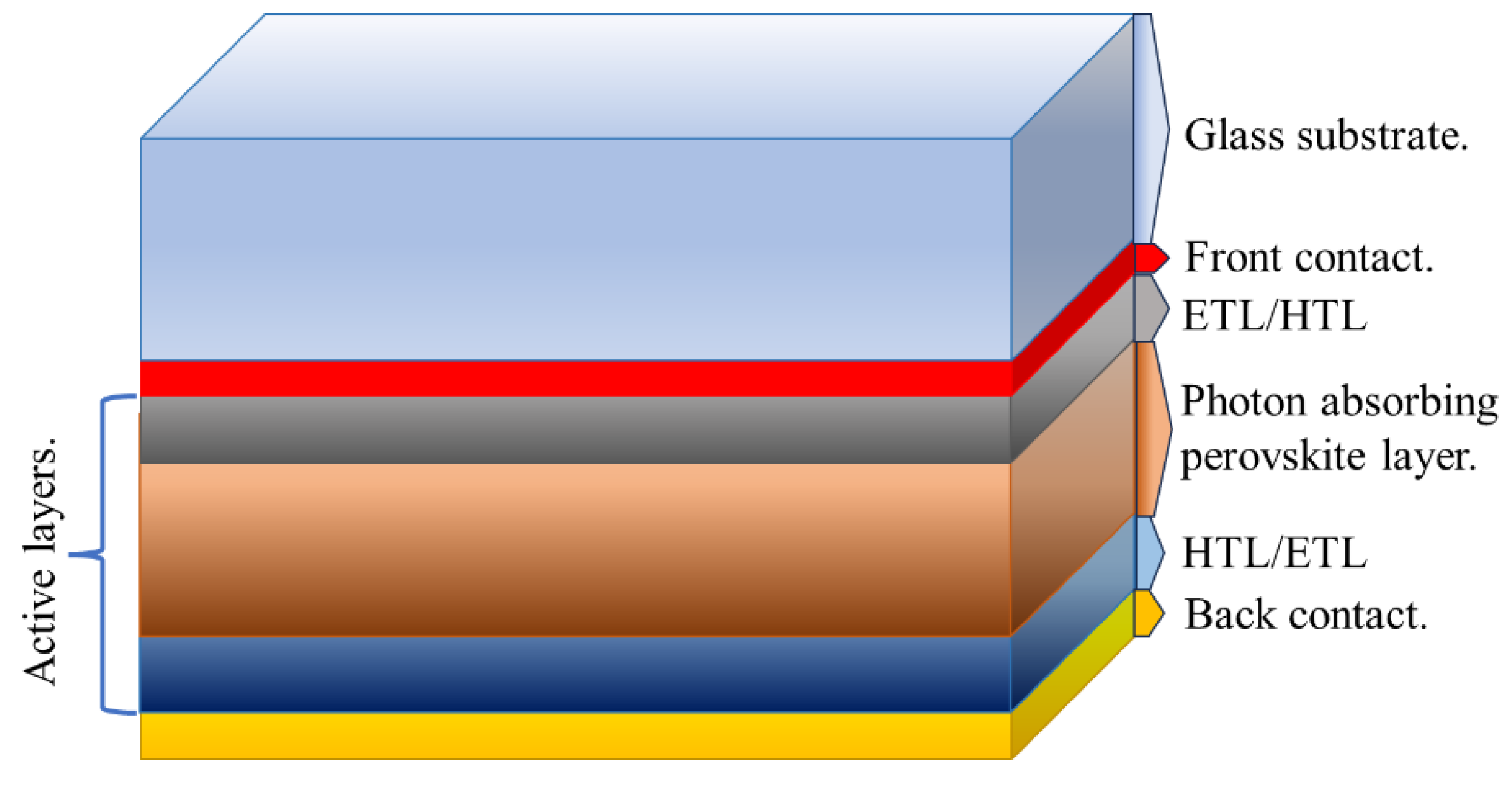
Figure 1. Layered structure of perovskite solar cell.
Preprints 114546 g001
Figure 2. XRD plots of CuO thin films deposited at various annealing temperatures.
Preprints 114546 g002
Figure 3. Dependence of crystallite size, dislocation density, and microstrain on annealing temperature.
Preprints 114546 g003
Figure 4. Raman spectra of CuO thin films annealed at different temperatures.
Preprints 114546 g004
Figure 5. Transmission patterns of CuO thin films annealed at various temperatures.
Preprints 114546 g005
Figure 6. Plots of absorption coefficient versus wavelength for CuO thin films.
Preprints 114546 g006
Figure 7. (a) Plots of α h v 2 vs incident light energy ( h v ); (b) Inset; Tauc plots of CuO thin films deposited at various annealing temperatures.
Preprints 114546 g007
Figure 8. FTIR plots of CuO thin films annealed at various annealing temperatures.
Preprints 114546 g008
Figure 9. SM surface view picture of CuO thin films fabricated at various annealing temperatures.
Preprints 114546 g009
Figure 10. Conductivity type determination; (A) Reference n-type Si substrate, (B) CuO thin film sample. Inset; Measurement set-up.
Preprints 114546 g010
Figure 11. Resistivity values for different CuO films annealed at various temperatures.
Preprints 114546 g011
Table 1. Structural parameters of CuO thin films obtained from XRD spectra.
Method Temperature T(°C) FWHM 2θ (Degree) Crystallite size D(nm) Micro strain ε(10-4) Dislocation density δ(1014/m2) Reference
Drop casting 200 0.2160 40.70 8.64 6.22 [39]
Plasma focus RT 0.1710 122.6 0.28 0.6 [39]
Spin coating 600 0.2334 37.68 9.61 7.04 [40]
Spin coating 200 0.1850 44.54 3.88 5.04 Present work
Spin coating 250 0.1738 47.60 3.64 4.41 Present work
Spin coating 300 0.1694 49.27 3.51 4.11 Present work
Spin coating 400 0.1529 54.14 3.20 3.41 Present work
Table 2. Raman shift for different annealing temperatures.
Annealing temperature (°C) Raman shift (cm-1) Phonon mode Corresponding mode Reference
450 624.00 B g 2 CuO [43]
250 89.00 Ag CuSbSe2 [44]
500 286.00 Ag CuO [45]
450 292.00 Ag CuO [6]
200 304.93 Ag CuO Present work
250 301.12 Ag CuO Present work
300 295.41 Ag CuO Present work
400 299.22 Ag CuO Present work
Table 3. Bandgap of CuO thin films for various annealing temperatures.
Deposition Method Annealing temperature (°C) Band gap energy (eV) Reference
Chemical spray pyrolysis 400 – 600 2.60 – 2.45 [53]
Spin coating 250 – 450 3.99 – 3.94 [54]
Spin coating 300 – 700 1.64 – 1.46 [55]
Spin coating 300 – 500 2.70 – 1.80 [27]
Spin coating 450 – 550 3.72 – 3.48 [56]
Spin coating RT – 600 1.61 – 1.44 [57]
Spin coating 150 – 500 1.62 – 1.43 [58]
Spin coating 250 – 400 1.93 – 1.81 Present work
Table 4. FTIR band positions and assignments.
Band position (cm-1) Assigned group or stretching/ bending Reference
646 Cu-O [65]
455 Cu-O [66]
443,535 Cu-O [67]
784 Cu-O [62]
420,503,615,740 Cu-O [68]
446,759,764 Cu-O Present work
Table 5. Electrical data of the CuO thin films annealed at different temperatures.
Annealing- temperature (°C) 200 250 300 400
Conductivity type P P P P
Carriers type Holes Holes Holes Holes
Sheet Resistance (Ω) 8221.2 6711.2 5872.3 6543.4
Resistivity (Ω.cm) 0.1554 0.1208 0.1028 0.1152
Conductivity (Ω.cm)-1 6.4358 8.27803 9.7039 8.68325
Disclaimer/Publisher’s Note: The statements, opinions and data contained in all publications are solely those of the individual author(s) and contributor(s) and not of MDPI and/or the editor(s). MDPI and/or the editor(s) disclaim responsibility for any injury to people or property resulting from any ideas, methods, instructions or products referred to in the content.
Copyright: This open access article is published under a Creative Commons CC BY 4.0 license, which permit the free download, distribution, and reuse, provided that the author and preprint are cited in any reuse.
Prerpints.org logo

Preprints.org is a free preprint server supported by MDPI in Basel, Switzerland.

Subscribe

© 2024 MDPI (Basel, Switzerland) unless otherwise stated