1. Introduction
Since the thickness of TMD can be pushed down to less than a few nanometers, TMD is promising alternative channel materials for realizing ultra-thin body field effect transistors (FET) which are robust to short channel effects. TMD is divided into two kinds of crystal structures of trigonal prismatic (2H-TMD type) and octahedral (1T-TMD type). MoS
2 is typical TMD with a 2H-TMD type structure. TMD with the 1T-TMD type (group space P3m1) structure has a much lower lattice thermal conductivity and a better thermoelectric performance at room temperature. This implies that HfS
2 is a good 2D thermoelectric material. Hao Wang et al. predicted that the lattice thermal conductivity of bulk HfS
2 is much smaller than it of MoS
2, making the HfS
2 system a promising thermoelectric material [
1]. They also investigated the thermoelectric properties of monolayer HfS
2 and demonstrated that monolayer HfS
2 is an excellent n-type thermoelectric material, with much improved thermoelectric performance compared with the bulk. Furthermore, the valence band valleys in monolayer HfS
2 can be tuned by the external biaxial tensile strain owing to the degeneracy of the valence band valleys reaching the maximum at strain value of 6%. Monolayer HfS
2 like CdI
2-type structure has become well-known due to its low lattice thermal conductivity resulting in promising applications in thermoelectric [
2]. Hongyan Guo et al. performed a systematic first-principles study of the effect of tensile strains on the electronic properties of early monolayer TMD and suggested that the tensile strain could significantly affect the electronic properties of many early TMDs in general and the electronic bandgap in particular [
3]. For group IVB TMD such as HfS
2, the bandgap increased with the biaxial tensile strain while starting to decrease at strain 6~8%. Their investigation suggested that strain engineering was an effective approach to modify electronic properties of TMD such as monolayer HfS
2, thereby opening an alternative way for future electronic applications. Recently, Mayuri Sritharan et al. pointed out that transition metal dichalcogenides (TMD) monolayers with native high-
κ oxides presented a new avenue towards the development of new generation field-effect transistor (FET) devices [
4]. These TMD materials experimentally showed to form a natively compatible high dielectric oxide layer, which could enhance both transistor device scaling and the supply voltage shrinking. They found that monolayer hafnium disulphide (HfS
2) exhibited isotropic transport at channel length of 10 nm with ON currents over 1000 μA/μm and good subthreshold swing and identified monolayer HfS
2 as a superior material within this TMD family for ultra-scaled FET.
Dr. A. Afzalian’s research team from imec developed an atomistic-modelling solver (ATOMOS) to assess the physics and fundamental-performance potential of monolayer HfS
2 FET down to a gate length of 5 nm, including the effect of carrier phonon scattering [
5,
6]. They predicted that the monolayer HfS
2 FET had good scalability down to gate length of 5 nm with a promising high on current level. They also proposed a concept of dynamically doped 2D FET, that scaled better than other 2D FET counterpart. Used in the combination with a best mobility material such as monolayer HfS
2, it allowed for keeping the excellent performance on drive current and competitive energy-delay. In Ref. [
7], Dr. Jiwon Chang investigated ballistic transport characteristics of monolayer HfS
2 FET via quantum transport simulation. He focused on the role of degenerate conduction band (CB) valleys in monolayer HfS
2 and predicted that the effect of channel orientation on device performances was much weaker in monolayer HfS
2 FET owing to the degenerate CB valleys of monolayer HfS
2.
Toru Kanazawa et al. first experimentally evaluated the FET performance of HfS
2 and revealed its potential for transistor channel [
8]. In addition, the other properties of HfS
2 were not thoroughly investigated and they also reported some basic characteristics of HfS
2 essential for FET device fabrication. Continuous efforts to seek for other 2-D materials lead to the discovery of anisotropic 2-D material. Unlike Mo-based TMD, HfS
2 is characterized with its highly anisotropic conduction band. Theoretical investigations of HfS
2 FETs have been performed [
5,
6,
7]. Anisotropic 2-D materials other than phosphorene, Hf-based TMDs, have been explored by density functional theory (DFT) calculations [
9,
10]. Monolayers of Hf-based TMD such as HfS
2, are quite different from those of Mo-based TMD because of different crystal symmetry and atomic bonding. They have indirect band gaps with three-fold degenerate conduction band (CB) valleys whose dispersions around the minimum of CB are highly anisotropic. Among Hf-based TMDs, monolayer HfS
2 exhibits sizable band gaps, larger than 1 eV, suitable for nanoscale FET applications. In this work, we present a comprehensive computational study of carrier mobility of monolayer HfS
2 through the first principle method, compact band model and Kubo-Greenwood mobility approach. We discuss the influence of band structure anisotropy of monolayer HfS
2 on carrier transport performances as well as the strain engineering of monolayer HfS
2.
As a member of 1T-MX2, the carrier transport performance of monolayer HfS2 deserves to be further explored and improved. Although its carrier transport performance has been reported, there is few studies about the effects of the strain on this topic. Strain effects on materials can tune their electronic band degeneracy and thus broaden carrier transport properties. In the present work, we use DFT accompanied by Boltzmann transport theory and deformation potential theory to study the strain effect on the carrier transport properties of monolayer HfS2. The results indicate that the carrier effective mass is highly shrinking when the biaxial compressive strain gets 4%. As a consequence, the carrier mobility reaches the highest value for both electron and hole. In this case, we surprisingly discovery that the highest mobility value is owing to carrier effective mass shrinking.
The effect of strain on the band structure and bandgap of monolayer HfS
2 has been investigated in previous studies [
11,
12], showing that the application of tensile and compressive biaxial strain results in bandgap increasing and decreasing, respectively. Manouchehr Hosseini et al. studied the effect of strain on the mobility of monolayer MoS
2 and found that the tensile biaxial strain could significantly enhance the mobility [
13]; however, the investigation of a strain effect on the mobility of other 1T-TMD such as HfS
2 was still missing. The conduction and valence band structures of HfS
2 are different owing to indirect bandgap and the conduction band and valence band having different effective masses. In this work, we present a comprehensive analysis on the effect of biaxial strain on the mobility of monolayer HfS
2, employing the first principle method for band structure calculations and then the Kobo-Greenwood mobility approach for evaluating carrier mobility [
14,
15]. The methodology for first principle method, compact band model, and Kobo-Greenwood mobility approach is briefly presented in
Section 2. The effects of biaxial strain on the band structure and mobility of monolayer HfS
2 are discussed in
Section 3, and the concluding works are presented in
Section 4.
3. Results and Discussion
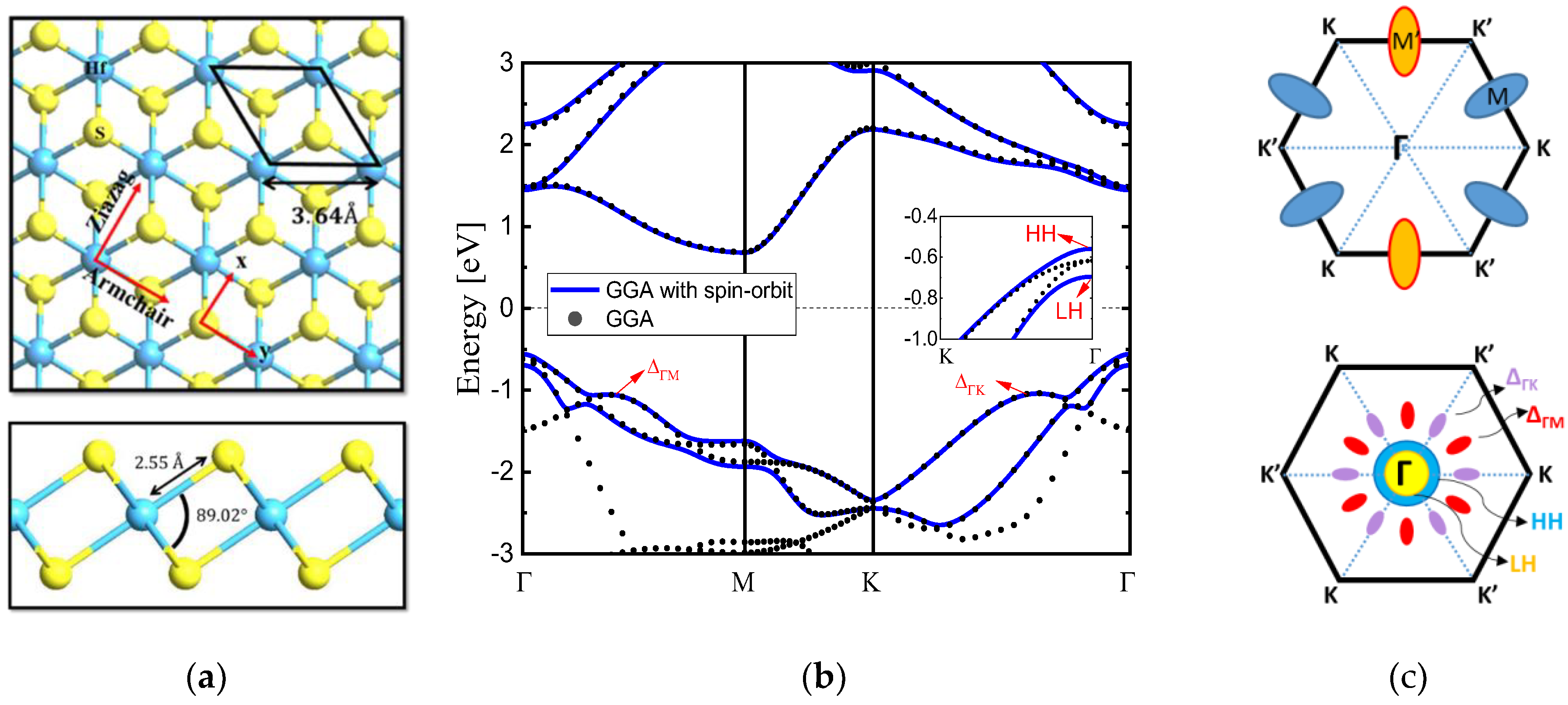
In an unstrained monolayer HfS
2 the lowest minima in the conduction band are denoted as M’-valley and M-valley in
Figure 1b, respectively. One M’ valley and two M valleys are degenerate for unstrained and biaxial strain conditions. With the application of biaxial strain, however, they do not split into 1 M’-valley and 2 M-valleys with different effective masses and energy minima. For the valence band of unstrained monolayer HfS
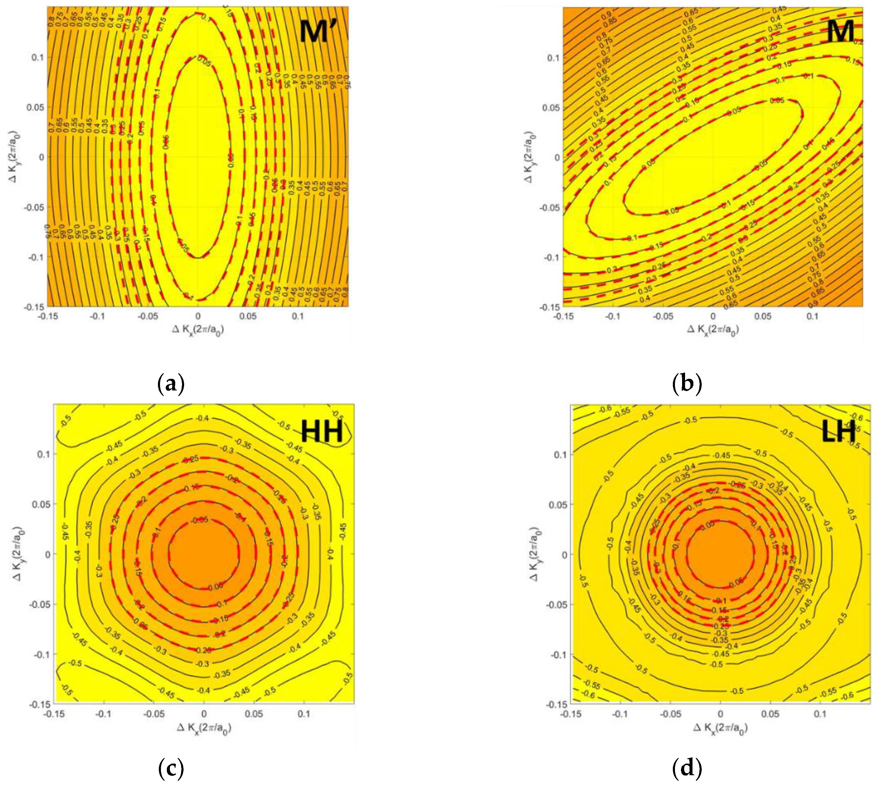
2 the top two bands are denoted as HH-band and LH-band, respectively. Energy contour plots for conduction band and valence band of monolayer HfS
2 in the 1
st BZ by ab-initio band structure calculation using GGA with spin-orbit coupling are shown in
Figure 2. Conduction band likes a valley with a parabolic elliptic energy dispersion. For valence band, LH looks like an isotropic parabolic band while HH is six-fold symmetry band. We further investigate the band structure close to the conduction and valence bands via contour plot which shows the constant energy lines. The contours around HH and LH bands are almost isotropic and circular at low energy, whereas M’ and M valleys demonstrate anisotropic behavior and are close to ellipsoid. A strong anisotropy of the constant energy lines can be seen around M points in the conduction band, due to the d orbit of Hf atom, while in the valence band lines in low energy region are almost isotropic. While the valence bands including HH and LH show almost isotropic dispersion, a strong anisotropic one occurs in the conduction band around M’ and M points due to the difference of the orbital structures of the valence (p orbit of S atom) and conduction bands.
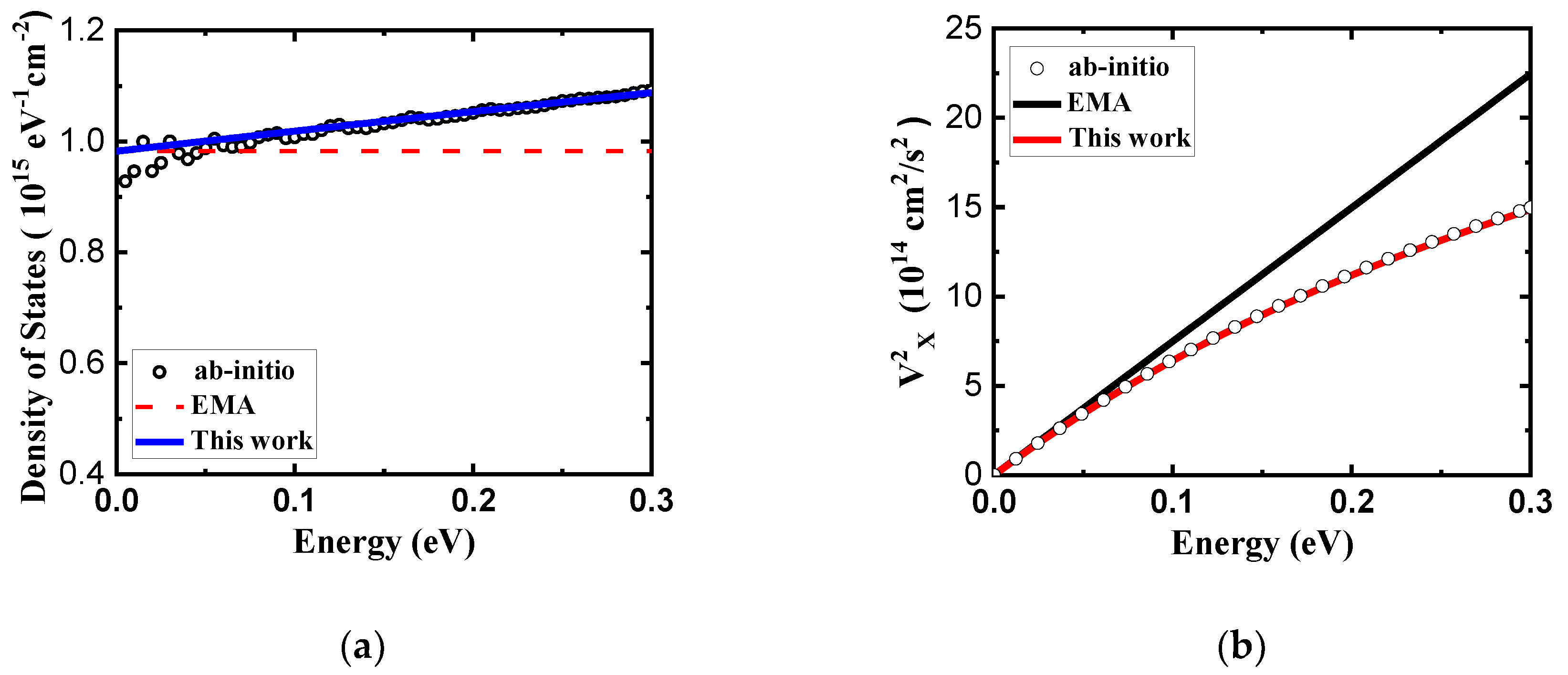
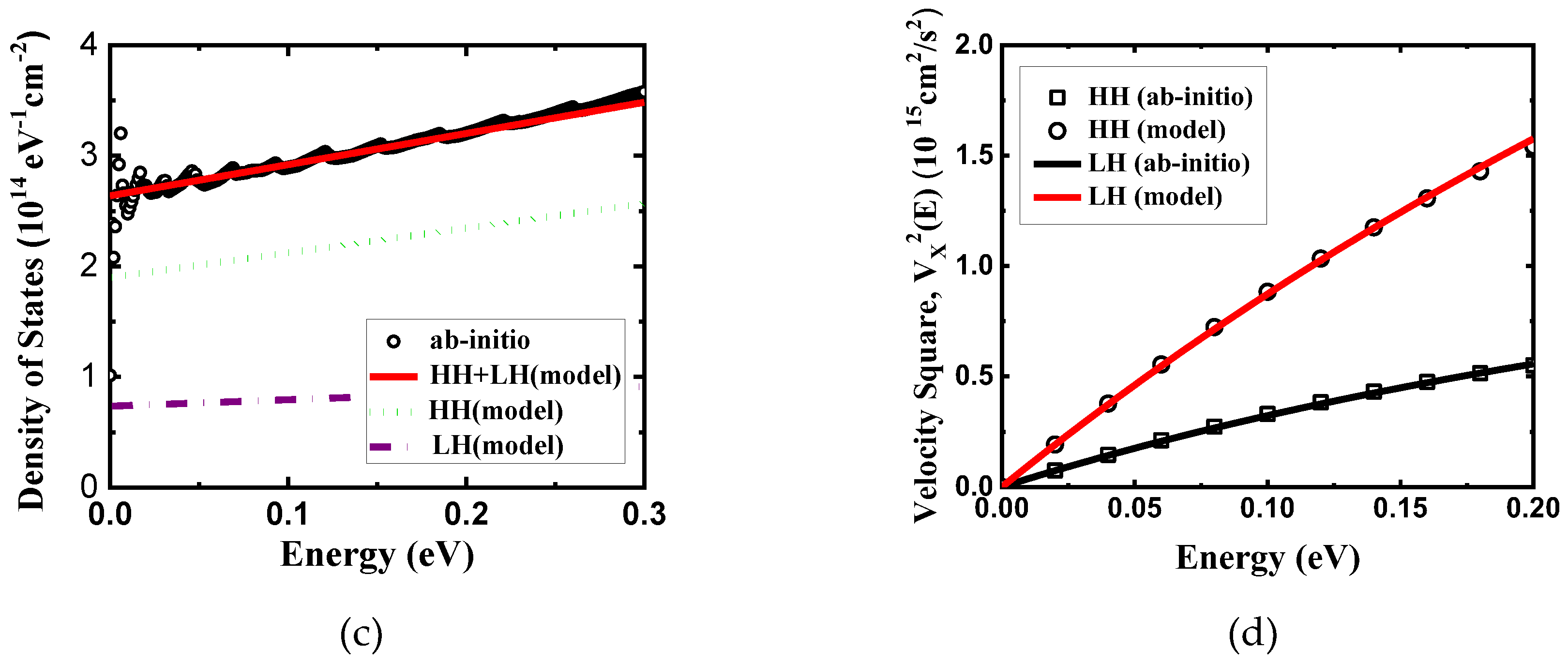
In
Figure 3, we present density of states and velocity square of monolayer HfS
2 using compact band models and ab-initio calculations. As you can see, our model can fit very well with ab-initio results, implying that our model is better than EMA model for carrier mobility calculation.
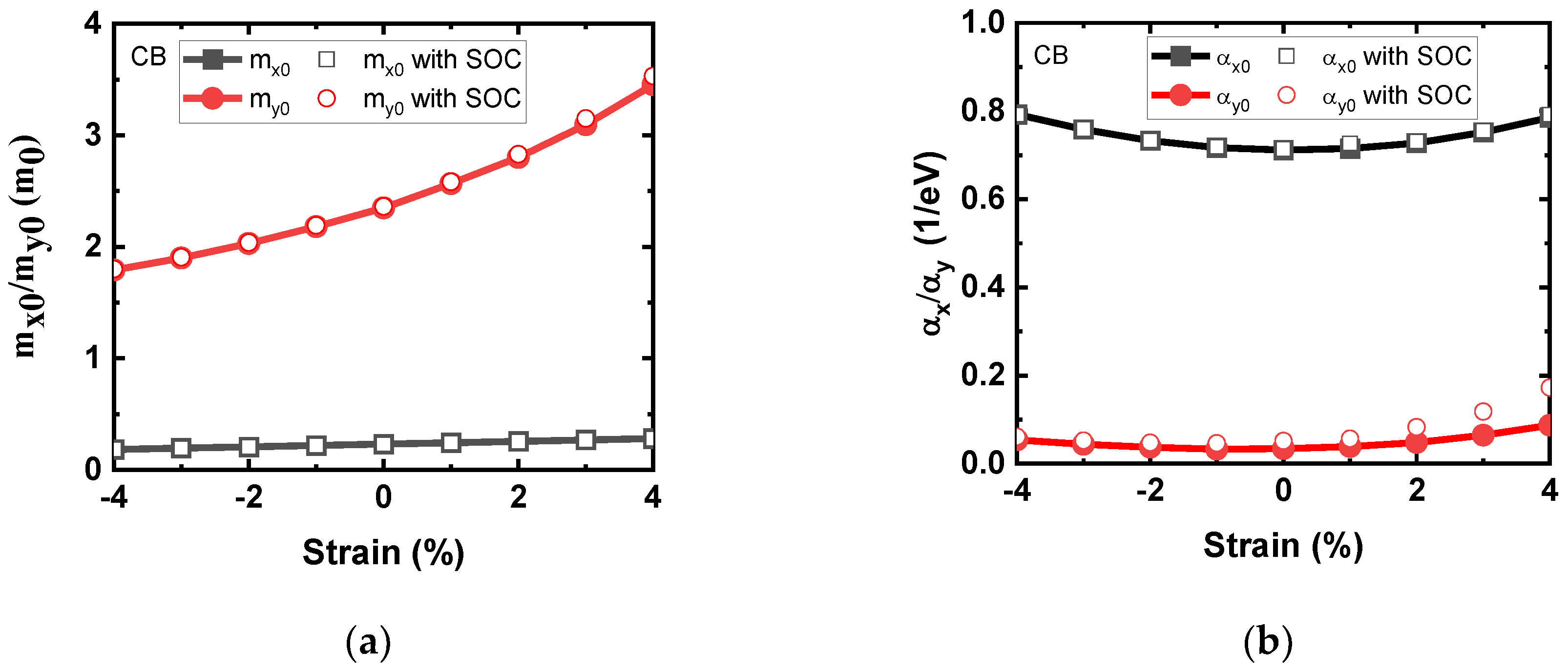
Key parameters including the effective masses and non-parabolicity factors of conduction band and valence band compact models under biaxial strain are shown in
Figure 4. Effective mass and also the non-parabolicity factor of Rudenko model are extracted from the DFT-calculated band structure and reported in
Figure 4a,b. In conduction band, two different paths at M’ valley demonstrate different effective masses. We denote with m
y0 the effective mass in the armchair direction (M’-Г) and with m
x0 the effective mass along the zigzag direction (i.e. M’-K). As it can be seen, m
y0 in M’ valley is ~ 10x larger than m
x0. Non-parabolicity factor α
y is very small as compared with α
x and slightly increases with increasing tensile strain. Difference of two effective masses in M’ valley increases with a rise in the strain and M’ valley shows more anisotropy for tensile strains. At the same time, the effective mass of M’ valley decreases with the strain and becomes the lowest effective mass at compressive biaxial strain of 4%. In
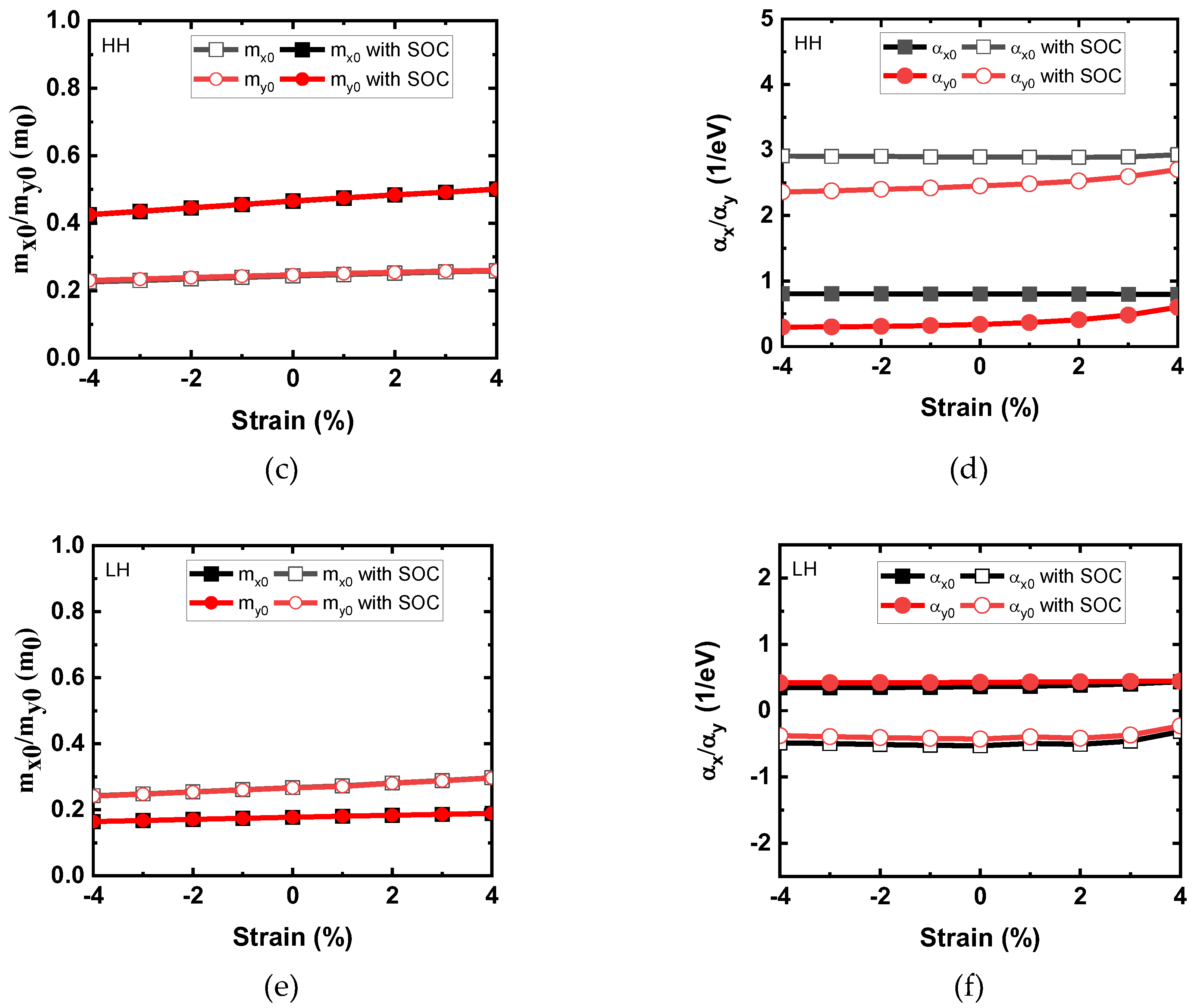
Figure 4c,d, key parameters of new compact band model are also extracted from ab-initio valence band HH structure. In
Figure 4e,f, key parameters of new compact band model are also extracted from ab-initio valence band LH structure. Effective mass decreases with increasing biaxial compressive strain for both CB and VB models while increases with increasing biaxial tensile strain. The hole effective mass has been explored under various strains. Two HH and LH bands, contribute to the major VB in the most range of strain. The HH and LH exhibit the lowest effective mass at compressive biaxial strain and one can find that the top VB is located at HH band in this strain range. The values of the HH band effective masses increase as the biaxial strain changes from compressive to the tensile regime.
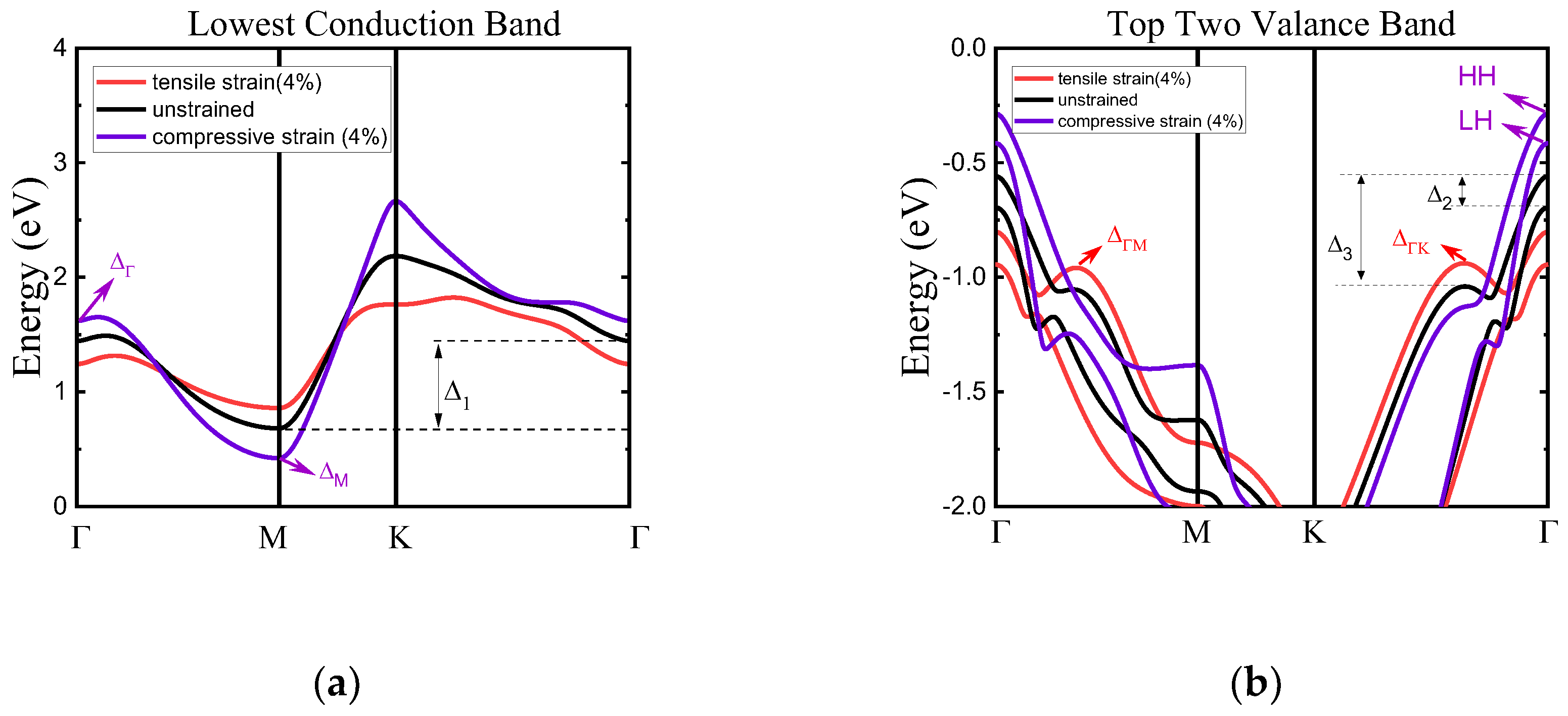
Figure 5 illustrates the band structure of unstrained and strained monolayer HfS
2 including lowest conduction band M valley and top two highest valence bands (HH and LH). The band structure is plotted for five strains, -4%, -2%, 0%, 2% and 4%. For unstrained one, M valley is lower than other valleys and located at the conduction band minimum (CBM). Note that M valley is still dominant at all strain region. As one can see, the strain can modify shape and energy for each valley. Under biaxial strain, conduction band and valence band edges shift up and down with increasing strain, respectively. The energy distance between these M-valley and Г-valley for unstrained material is evaluated to be ~720 meV, in agreement with Refs. [
4,
11]. Biaxial compressive strain increases this energy distance, which is instead reduced by a tensile strain. This implies effective mass along M’-Г direction decreasing with increasing biaxial compressive strain. For valence band, HH and LH energy splitting at Г point owing to spin orbit coupling not being sensitive to strain. In particularly, a relatively large biaxial compressive strain shifts the band edge energy of HH band so that it becomes the top valence band as shown in
Figure 5b. Here we can anticipate that, while under compressive strain, one can neglect the scattering between HH band and △
ГM and △
ГK bands, and under tensile strain, this type of scattering can significantly degrade the hole mobility.
Strain from −4% to +4% is applied to band structure of monolayer HfS
2 in
Figure 6. The bandgap of monolayer HfS
2 as a function of biaxial strain is shown in
Figure 6a. The band gap of unstrained HfS
2 is 1.25 eV and in agreement with Refs. [
3,
25]. Strain dependent of the band gap from our work is in agreement with Ref. [
1,
11,
12]. It is well known that strain can modify the band structure. In this work, we find that the biaxial tensile strain leads to an increase in the band gap and a biaxial compressive strain leads to a decrease in the band gap. When the biaxial stress effect is from −4 to 4%, the band gap of the system increases from 0.65 to 1.67 eV. In
Figure 6b, absolute conduction band edge (E
c) and valence band edge (E
v) for ab-initio calculations use GGA with and without SOC as a function of biaxial strain. E
c is M valley and E
v is HH band. The energy in the bottom (top) of CB (VB) increases (decreases) respect to strain increase. As one can observe, both E
c and E
v almost change linear respect to biaxial strain, but the slope is opposite. SOC will cause the energy of E
v shifting up. We also find that the strain-induced modulation of E
c is relatively smaller than the modulation of E
v.
Figure 6c shows the variation of energy difference between Г and M valleys denoted as △
1 and valence band difference between HH band and △
ГK band (△
3) and HH-LH band splitting (△
2) under different biaxial strain, respectively.
According Ref. [
6], dynamical doping with the gate voltage of the 2D FET electrostatically induces a high carrier concentration and keeps higher carrier mobility of channel material monolayer HfS
2. We use carrier density of 6x10
12 cm
-2 in the following results of calculated carrier mobility.
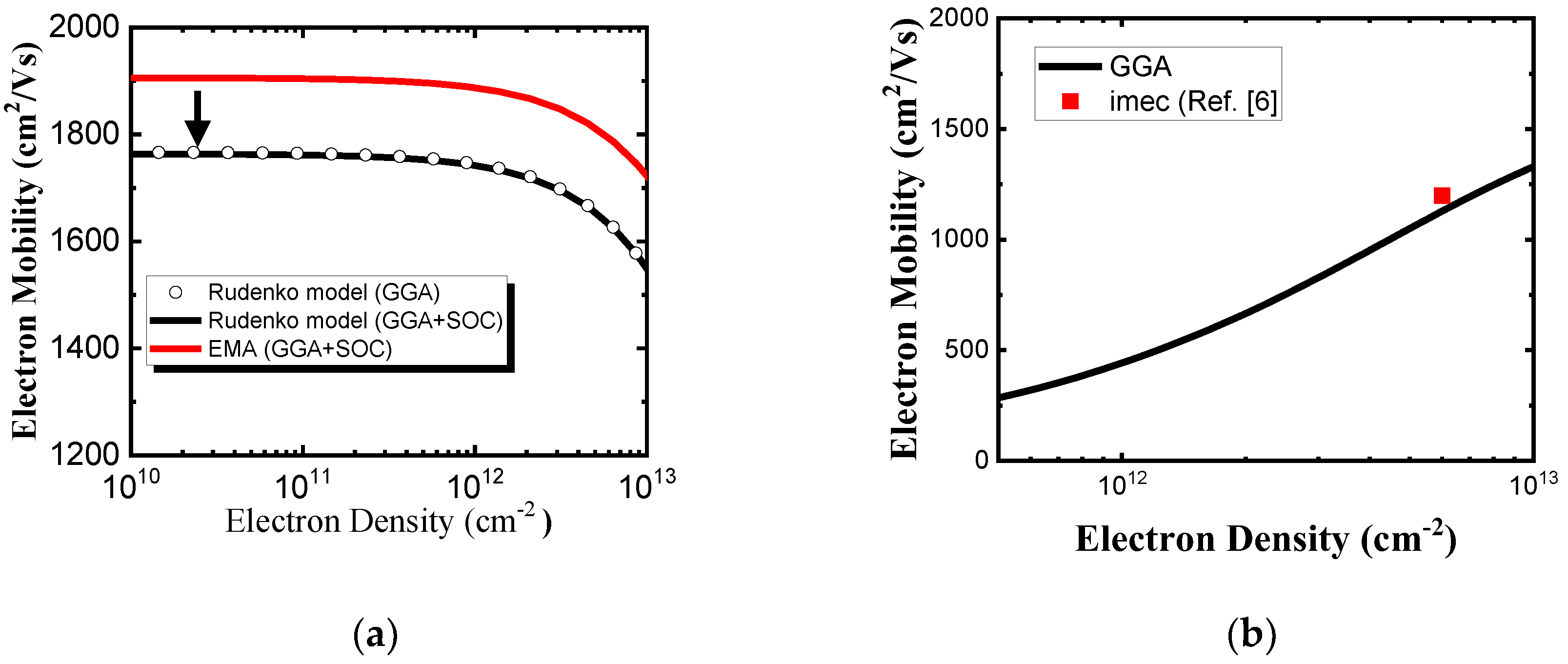
Figure 7a shows the room temperature electron mobility without polar optical phonon scattering versus electron density for the unstrained monolayer HiS
2 by two compact models. As you can see, calculated electron mobility by Reudenko model is lower than it by EMA model due to conduction band non-parabolicity effect. It implies that non-parabolicity effect is important in electron mobility calculation and can’t be ignored. SOC almost does not change conduction band from ab-initio GGA calculation and results in calculated electron mobilities are the same from Rudenko model which fits GGA ab-initio conduction bands with and without SOC. As can be seen in
Figure 7b, because of screening the electron mobility with polar optical phonon scattering increases with the electron density for monolayer HfS
2, our calculations are in agreement with the imec’s work [
6]. The biaxial strain-dependency of intrinsic phonon limited mobility is presented in
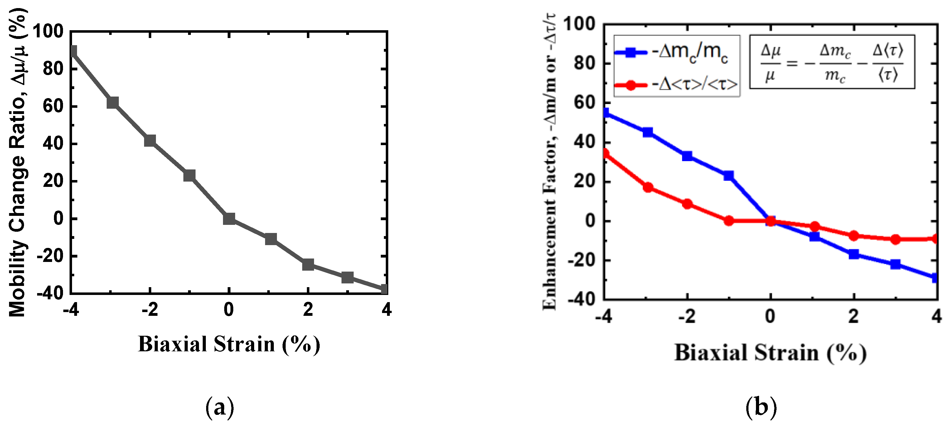
Figure 8a. Enhancement factors owing to -△m/m and -△τ/τ versus biaxial strain are shown in
Figure 8b. Apparently, the effects of compressive and tensile strain on electron mobility are very different, which can be mainly explained by considering the role of electron effective mass and scattering rate. For example, with biaxial compressive strain, the electron effective masses of M’ and M-valleys are much lower than that of unstained condition, which enhance electron mobility. Under biaxial tensile strain, instead, the electron effective mass of CB higher than the unstrained one. With biaxial compressive strain, the electron mobility increases because of the reduction of the electron effective mass and also results in the reduction of the scattering rate. With a biaxial compressive strain of 4%, the phonon limited mobility becomes 90% higher than that of unstrained material. In contrast, a biaxial tensile strain of 4% reduces the electron mobility ~40% as compared with unstrained one owing to the increase of both effective mass and scattering rate.
Figure 8 also indicates that the biaxial strain induced electron mobility enhancement with compressive strain is larger than that with tensile strain.
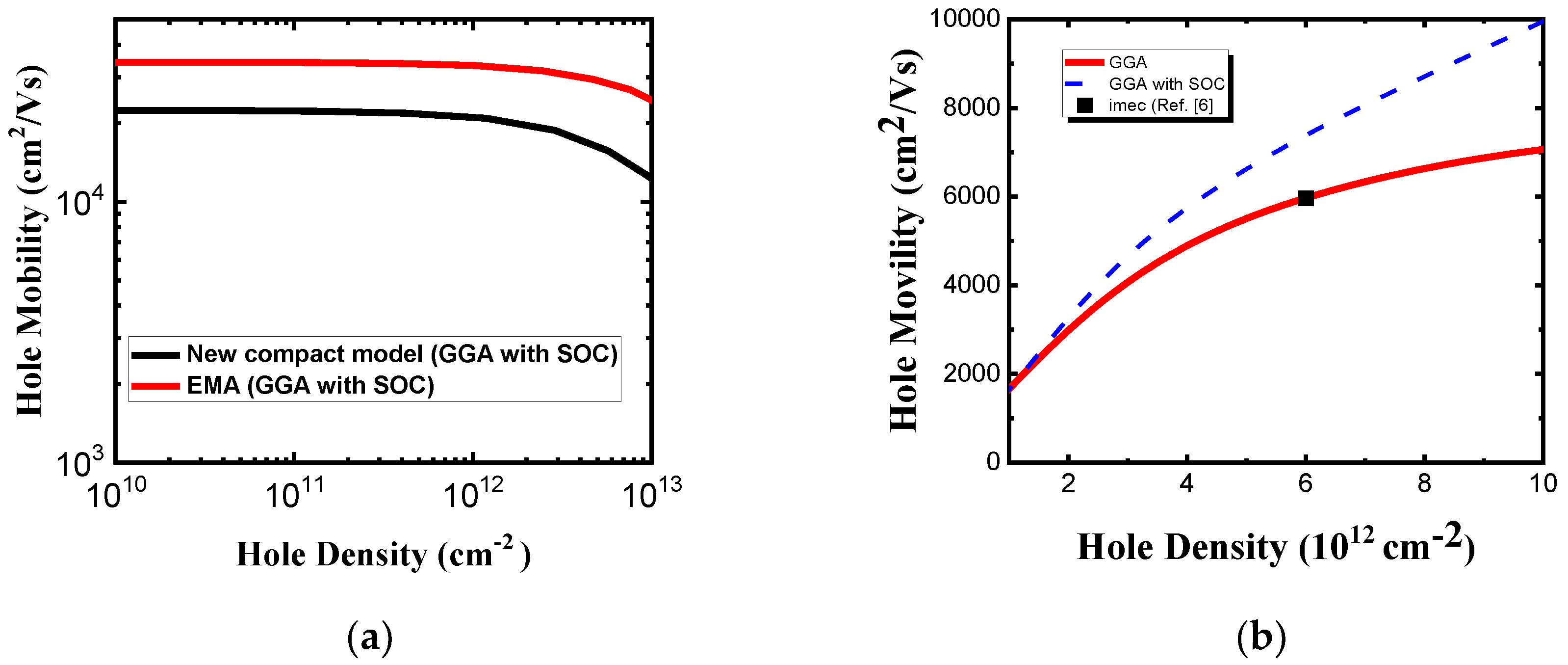
Figure 9a shows the room temperature hole mobility without polar optical phonon scattering versus hole density for the unstrained monolayer HiS
2 by two compact models. As you can see, hole mobility by new compact band model is lower than it by EMA model due to valence band non-parabolicity effect. It implies that non-parabolicity effect is important in hole mobility calculation and can’t be ignored. As can be seen in
Figure 9b, because of screening the hole mobility with polar optical phonon scattering increases with the hole density for monolayer HfS
2, our calculations are in agreement with the imec’s work [
6]. Note that SOC strongly affects HH and LH valence band degeneracy at Г point and causes valence band splitting. As you can see, calculated hole mobility by new compact model, which fits GGA ab-initio valence band structure with SOC, is higher than the one without SOC owing to HH and LH band splitting effect. Most holes are in HH band for GGA ab-initio valence band structure and effective mass shrinkage of HH owing to SOC. This is the major reason for calculated hole mobility results, as shown in
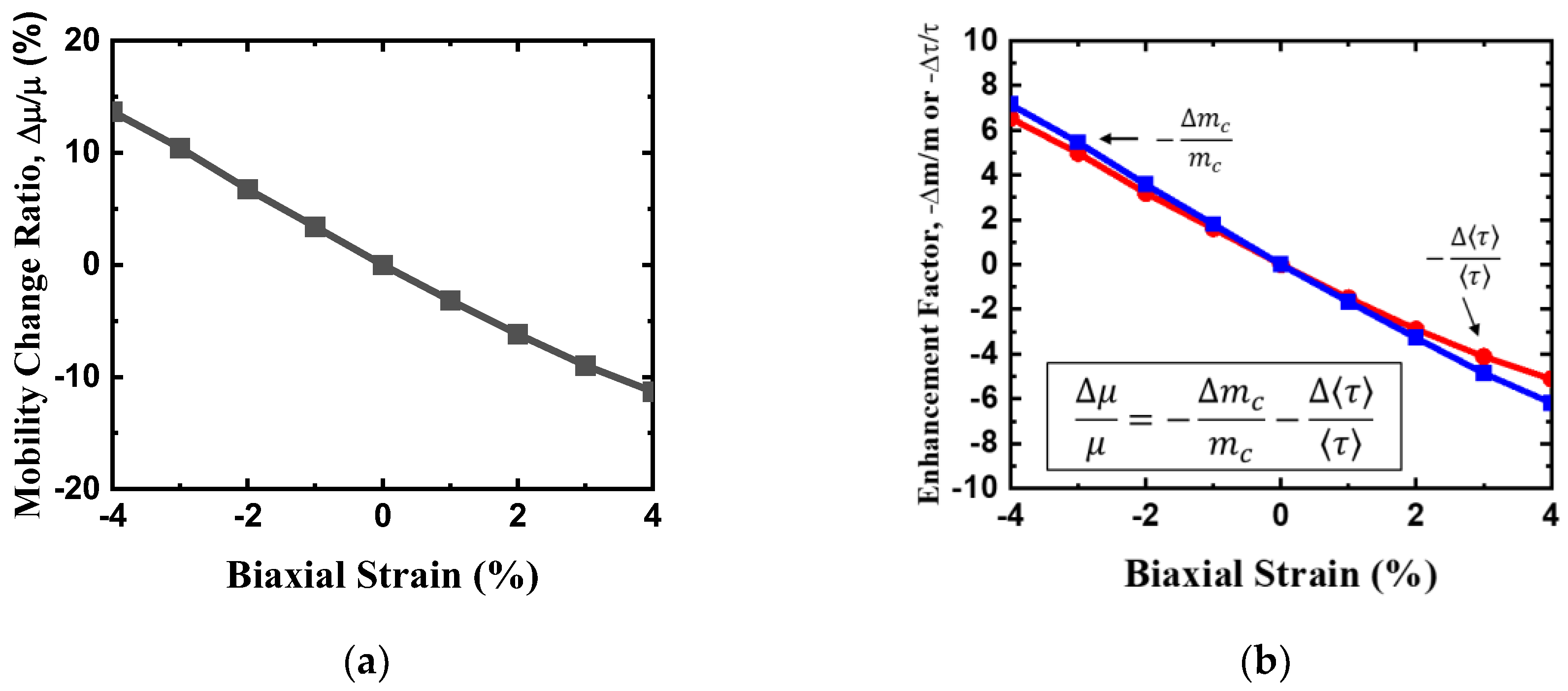
Figure 9b. The biaxial strain-dependency of intrinsic phonon limited hole mobility change ratio is presented in
Figure 10a. Enhancement factors of hole mobility owing to -△m
c/m
c and -△<τ>/<τ> versus biaxial strain are shown in
Figure 10b. Relation between hole mobility change ratio and enhancement factors is included for your reference in the inset. Apparently, the effects of compressive and tensile biaxial strain on hole mobility are very different, which can be mainly explained by considering the role of hole effective mass and scattering rate. For example, with biaxial compressive strain, the effective masses of HH and LH bands are much lower than that of unstained condition, which enhance hole mobility. Under biaxial tensile strain, instead, the hole effective mass of VB is higher than the unstrained one. In the biaxial strain range from -4% to 4%, hole interband scattering owing to HH band and satellite bands such as △
ГM and △
ГM is not serious and can be ignored. Moreover, when biaxial tensile strain is >4%, it increases the valence band degeneracy of monolayer HfS
2 even more, and the degenerate valence bands and higher interband phonon scattering rate lead to a very low hole mobility. With biaxial compressive strain, the hole mobility increases because of the reduction of the hole effective mass and also results in the reduction of the scattering rate. With a biaxial compressive strain of 4%, the phonon limited mobility becomes ~13% higher than that of unstrained material. In contrast, a biaxial tensile strain of 4% reduces the hole mobility ~11% as compared with unstrained one owing to the increase of both hole effective mass and scattering rate.
Figure 1.
(a) Top and side (bottom) views of monolayer HfS2 showing a primitive hexagonal unit cell (Blue: Hf atoms; Yellow: S atoms) (b) Band structures of monolayer HfS2 along the high symmetric points in the hexagonal BZ. Spin-orbit coupling splits valence band HH and LH as shown in the inset. (c) Three lowest conduction band valleys are located at M’(M) points, six △ГM (red) and six △ГK (purple) bands in the corresponding 1st BZ with high symmetric points.
Figure 2.
Energy contour plots for (a) M’ valley, (b) M valley, (c) HH band, and (d) LH band of monolayer HfS2. Note that M’ and M valleys are CB while HH and LH bands are VB. Here Energy contour plots is based on ab-initio band structure calculation using GGA with spin-orbit coupling. Dash lines are calculated results from compact band models including Rudenko model and new compact model.
Figure 3.
(a) Density of states and (b) velocity square as a function energy for M’ valley of monolayer HfS2, respectively. (c) Density of states and (d) velocity square as a function energy for valence band of monolayer HfS2, respectively. Above calculations are based on ab-initio GGA band structure.
Figure 4.
Key parameters including (a) effective mass and (b) non-parabolicity factor of Rudenko model for conduction band of monolayer HfS2 under biaxial strain. Key parameters including (c) effective mass and (d) non-parabolicity factor of new compact model for valence band HH of monolayer HfS2 under biaxial strain. Key parameters including (e) effective mass and (f) non-parabolicity factor of new compact model for valence band LH of monolayer HfS2 under biaxial strain.
Figure 5.
The change of (a) lowest conduction band and (b) top two highest valence band of monolayer HfS2 under compressive and tensile biaxial strains as calculated by ab-initio method with GGA considering SOC.
Figure 5.
The change of (a) lowest conduction band and (b) top two highest valence band of monolayer HfS2 under compressive and tensile biaxial strains as calculated by ab-initio method with GGA considering SOC.
Figure 6.
(a) The variation of bandgap of monolayer HfS2 under biaxial strain. (b) Absolute conduction band edge (Ec) and valence band edge (Ev) for ab-initio calculations with GGA considering SOC or not as a function of biaxial strain. (c) Energy difference between conduction band (△1) and valence band valleys (△2 and △3) versus biaxial strain.
Figure 7.
(a) Phonon-limited electron mobility without polar optical phonon scattering versus electron density with two compact band models for monolayer HfS
2. (b) Electron mobility with polar optical phonon scattering as a function of electron density. Square symbol is imec’s calculated data from Ref. [
6].
Figure 8.
(a) Electron mobility change ratio as a function of biaxial strain. (b) Enhancement factors ( and ) versus biaxial strain.
Figure 8.
(a) Electron mobility change ratio as a function of biaxial strain. (b) Enhancement factors ( and ) versus biaxial strain.
Figure 9.
(a) Phonon-limited hole mobility without polar optical phonon scattering versus hole density with two compact band models for monolayer HfS
2. (b) Hole mobility with polar optical phonon scattering as a function of hole density. Square symbol is imec’s calculated data from Ref. [
6].
Figure 9.
(a) Phonon-limited hole mobility without polar optical phonon scattering versus hole density with two compact band models for monolayer HfS
2. (b) Hole mobility with polar optical phonon scattering as a function of hole density. Square symbol is imec’s calculated data from Ref. [
6].
Figure 10.
(a) Hole mobility change ratio as a function of biaxial strain. (b) Enhancement factors ( and )versus biaxial strain.
Figure 10.
(a) Hole mobility change ratio as a function of biaxial strain. (b) Enhancement factors ( and )versus biaxial strain.
Table 1.
The effective mass for CB and VB of monolayer HfS2 by ab-initio calculation with GGA and GGA+SOC, respectively.
Table 1.
The effective mass for CB and VB of monolayer HfS2 by ab-initio calculation with GGA and GGA+SOC, respectively.
| GGA |
| Valley/band |
mMГ/mAR (m0) |
mMK/mZA(m0) |
mDOS=(mMГmMK)1/2 (m0) |
| M’ valley |
2.36 |
0.23 |
0.74 |
| M valley |
0.3 |
0.71 |
0.74 |
| |
mГM (m0) |
mGK (m0) |
mDOS = (mГMmГK)1/2(m0) |
| HH band |
0.47 |
0.47 |
0.47 |
| LH band |
0.18 |
0.18 |
0.18 |
| GGA+SOC |
| Valley/band |
mMГ/mAR (m0) |
mMK/mZA(m0) |
mDOS=(mMГmMK)1/2 (m0) |
| M’ valley |
2.35 |
0.23 |
0.74 |
| M valley |
0.3 |
0.71 |
0.74 |
| |
mГM (m0) |
mGK (m0) |
mDOS = (mГMmГK)1/2(m0) |
| HH band |
0.25 |
0.24 |
0.24 |
| LH band |
0.27 |
0.27 |
0.27 |
Table 2.
The new compact model parameters for CB of monolayer HfS2.
Table 2.
The new compact model parameters for CB of monolayer HfS2.
| GGA |
|
|
|
|
|
|
|
|
|
| |
GGA+SOC |
|
|
|
|
|
|
|
|
|
|
Table 3.
The new compact model parameters for HH/LH VB of monolayer HfS2.
Table 3.
The new compact model parameters for HH/LH VB of monolayer HfS2.
| GGA |
|
HH/LH |
HH/LH |
|
|
|
|
|
|
| |
GGA+SOC |
|
|
HH/LH |
HH/LH |
|
|
|
|
|
|
Table 4.
The effective mass, deformation potential constant of electron and hole for unstrained monolayer HfS2 by ab-initio calculation with GGA.
Table 4.
The effective mass, deformation potential constant of electron and hole for unstrained monolayer HfS2 by ab-initio calculation with GGA.
| Carriers |
mMГ/mHH (m0) |
mMK/mLH (m0) |
Dac (eV) |
Dop (108eV/cm) |
| electron |
2.36 |
0.23 |
1.31 |
0.99 |
| hole |
0.47 |
0.18 |
0.95 |
0.73 |
