Submitted:
13 August 2024
Posted:
14 August 2024
You are already at the latest version
Abstract
Keywords:
1. Introduction
2. Materials and Methods
2.1. Datasets
2.2. Improved YOLOv5 algorithm
2.3. Feature Extraction Module Improvement
2.3.1. GhosetNet
2.3.2. CBAM Attention Mechanism
2.4. Lightweight Improvement Methods
2.4.1. Lightweight High-Resolution Prediction Network
2.4.2. Context-Aware Networks
2.5. SioU Loss Function
3. Experiments and Results
3.1. Feature extraction module comparison experiment
3.2. Comparison Experiment of Lightweight Improvement Methods
3.3. Ablation Experiment
3.4. Mainstream algorithm comparison experiment
3.5. Model Deployment and Calibration Detection Methods
3.5.1. Real-Time Detection Processing
3.5.2. Real-Time Anomaly Correction Method
3.5.3. Actual Detection Effect
4. Discussion
5. Conclusions
6. Patents
Author Contributions
Funding
Institutional Review Board Statement
Informed Consent Statement
Data Availability Statement
Acknowledgments
Conflicts of Interest
References
- Chen, M.-F., Y.-S. Ho, and S.-M. Wang. A fast positioning method with pattern tracking for automatic wafer alignment. in 2010 3rd International Congress on Image and Signal Processing. 2010. IEEE.
- Yang W and Xiao M, Research on Automatic Alignment System of Scribing Machine Based on Matlab. Mechanical Design and Manufacturing, 2012(05): p. 96-98.
- Wu, H., et al., Classification of solder joint using feature selection based on Bayes and support vector machine. IEEE Transactions on Components, Packaging and Manufacturing Technology, 2013. 3(3): p. 516-522. [CrossRef]
- Xu, J., et al., A wafer prealignment algorithm based on Fourier transform and least square regression. IEEE Transactions on Automation Science and Engineering, 2017. 14(4): p. 1771-1777. [CrossRef]
- Wang, Z., D. Zhou, and S. Gong, Uncalibrated visual positioning using adaptive Kalman Filter with dual rate structure for wafer chip in LED packaging. Measurement, 2022. 191: p. 110829. [CrossRef]
- Yu, N., Q. Xu, and H. Wang, Wafer defect pattern recognition and analysis based on convolutional neural network. IEEE Transactions on Semiconductor Manufacturing, 2019. 32(4): p. 566-573. [CrossRef]
- Chien, J.-C., M.-T. Wu, and J.-D. Lee, Inspection and classification of semiconductor wafer surface defects using CNN deep learning networks. Applied Sciences, 2020. 10(15): p. 5340. [CrossRef]
- Bian, Y.-C., et al. Using improved YOLOv5s for defect detection of thermistor wire solder joints based on infrared thermography. in 2021 5th International Conference on Automation, Control and Robots (ICACR). 2021. IEEE.
- Xu, J., et al., Chip Pad Inspection Method Based on an Improved YOLOv5 Algorithm. Sensors, 2022. 22(17): p. 6685. [CrossRef]
- He, K., et al. Deep residual learning for image recognition. in Proceedings of the IEEE conference on computer vision and pattern recognition. 2016.
- Huang, G., et al. Densely connected convolutional networks. in Proceedings of the IEEE conference on computer vision and pattern recognition. 2017.
- Howard, A.G., et al., Mobilenets: Efficient convolutional neural networks for mobile vision applications. arXiv preprint. arXiv:1704.04861, 2017.
- Sandler, M., et al. Mobilenetv2: Inverted residuals and linear bottlenecks. in Proceedings of the IEEE conference on computer vision and pattern recognition. 2018.
- Howard, A., et al. Searching for mobilenetv3. in Proceedings of the IEEE/CVF international conference on computer vision. 2019.
- Zhang, X., et al. Shufflenet: An extremely efficient convolutional neural network for mobile devices. in Proceedings of the IEEE conference on computer vision and pattern recognition. 2018.
- Ma, N., et al. Shufflenet v2: Practical guidelines for efficient cnn architecture design. in Proceedings of the European conference on computer vision (ECCV). 2018. [CrossRef]
- Ren, S., et al., Faster r-cnn: Towards real-time object detection with region proposal networks. Advances in neural information processing systems, 2015. 28.
- Girshick, R., et al. Rich feature hierarchies for accurate object detection and semantic segmentation. in Proceedings of the IEEE conference on computer vision and pattern recognition. 2014. [CrossRef]
- Liu, W., et al. Ssd: Single shot multibox detector. in Computer Vision–ECCV 2016: 14th European Conference, Amsterdam, The Netherlands, October 11–14, 2016, Proceedings, Part I 14. 2016. Springer.
- Redmon, J., et al. You only look once: Unified, real-time object detection. in Proceedings of the IEEE conference on computer vision and pattern recognition. 2016.
- Redmon, J. and A. Farhadi. YOLO9000: better, faster, stronger. in Proceedings of the IEEE conference on computer vision and pattern recognition. 2017.
- Redmon, J. and A. Farhadi, Yolov3: An incremental improvement. arXiv preprint. arXiv:1804.02767, 2018.
- Bochkovskiy, A., C.-Y. Wang, and H.-Y.M. Liao, Yolov4: Optimal speed and accuracy of object detection. arXiv preprint 2020. arXiv:2004.10934.
- Ultralytics, Yolov5. Available online: https://github.com/ultralytics/yolov5 (accessed on 22 February 2022).
- Zhu, X., et al. TPH-YOLOv5: Improved YOLOv5 based on transformer prediction head for object detection on drone-captured scenarios. in Proceedings of the IEEE/CVF international conference on computer vision. 2021. [CrossRef]
- Vaswani, A., et al., Attention is all you need. Advances in neural information processing systems, 2017. 30.
- Gong, H., et al., Swin-transformer-enabled YOLOv5 with attention mechanism for small object detection on satellite images. Remote Sensing, 2022. 14(12): p. 2861. [CrossRef]
- Lei, F., F. Tang, and S. Li,, Underwater target detection algorithm based on improved YOLOv5. Journal of Marine Science and Engineering, 2022. 10(3): p. 310. [CrossRef]
- Lu, S., et al., Swin-transformer-YOLOv5 for real-time wine grape bunch detection. Remote Sens 14: 5853. 2022. [CrossRef]
- Ling, Q., et al., Insulated Gate Bipolar Transistor Solder Layer Defect Detection Research Based on Improved YOLOv5. Applied Sciences, 2022. 12(22): p. 11469. [CrossRef]
- Zhang, S.G., et al., Swin-YOLOv5: Research and Application of Fire and Smoke Detection Algorithm Based on YOLOv5. Computational Intelligence and Neuroscience, 2022. 2022. [CrossRef]
- Liu, Z., et al. Swin transformer: Hierarchical vision transformer using shifted windows. in Proceedings of the IEEE/CVF international conference on computer vision. 2021.
- Han, K., et al. Ghostnet: More features from cheap operations. in Proceedings of the IEEE/CVF conference on computer vision and pattern recognition. 2020.
- Woo, S., et al. Cbam: Convolutional block attention module. in Proceedings of the European conference on computer vision (ECCV). 2018.
- Yu, F. and V. Koltun, Multi-scale context aggregation by dilated convolutions. arXiv preprint 2015. arXiv:1511.07122, 2015.
- Gevorgyan, Z., SIoU loss: More powerful learning for bounding box regression. arXiv preprint 2022. arXiv:2205.12740.
- Zheng, Z., et al. Distance-IoU loss: Faster and better learning for bounding box regression. in Proceedings of the AAAI conference on artificial intelligence. 2020.
- Hu, J., L. Shen, and G. Sun. Squeeze-and-excitation networks. in Proceedings of the IEEE conference on computer vision and pattern recognition. 2018.
- Wang, Q., et al. ECA-Net: Efficient channel attention for deep convolutional neural networks. in Proceedings of the IEEE/CVF conference on computer vision and pattern recognition. 2020.
- Tan, M., R. Pang, and Q.V. Le. Efficientdet: Scalable and efficient object detection. in Proceedings of the IEEE/CVF conference on computer vision and pattern recognition. 2020.
- Ge, Z., et al., Yolox: Exceeding yolo series in 2021. arXiv preprint 2021. arXiv:2107.08430.
- Yolov5-lite. Available online: https://github.com/ppogg/YOLOv5-Lite.
- Wang, C.-Y., I.-H. Yeh, and H.-Y.M. Liao, You only learn one representation: Unified network for multiple tasks. arXiv preprint 2021. arXiv:2105.04206.
- Wang, C.-Y., A. Bochkovskiy, and H.-Y.M. Liao. YOLOv7: Trainable bag-of-freebies sets new state-of-the-art for real-time object detectors. in Proceedings of the IEEE/CVF Conference on Computer Vision and Pattern Recognition. 2023.
- Zhu, P., et al., Detection and tracking meet drones challenge. IEEE Transactions on Pattern Analysis and Machine Intelligence, 2021. 44(11): p. 7380-7399.
- Yang, S., et al. Wider face: A face detection benchmark. in Proceedings of the IEEE conference on computer vision and pattern recognition. 2016.


| Method | Model | Parameters | FLOPs | mAP@0.5 |
|---|---|---|---|---|
| YOLOv5s | 13.75M | 7.0M | 16.0G | 0.867 |
| YOLOv5s-g | 11.57M | 5.8M | 12.6 | 0.872 |
| Method | rig | wro | Probe | mAP@0.5 |
|---|---|---|---|---|
| YOLOv5s-g +SE +ECA +CBAM |
0.913 0.917 0.918 0.914 |
0.853 0.849 0.855 0.873 |
0.851 0.858 0.856 0.851 |
0.872 0.875 0.876 0.879 |
| Method | rig | wro | Probe | mAP@0.5 | Model | Parameters | FLOPs |
|---|---|---|---|---|---|---|---|
| YOLOv5s-CBAM | 0.914 | 0.873 | 0.851 | 0.879 | 7.2M | 3.3M | 12.6G |
| YOLOv5s-HR | 0.918 | 0.892 | 0.844 | 0.884 | 3.25M | 1.27M | 10.2G |
| Method | rig | wro | Probe | mAP@0.5 |
|---|---|---|---|---|
| YOLOv5s-HR | 0.918 | 0.892 | 0.844 | 0.884 |
| +CSPP | 0.919 | 0.893 | 0.852 | 0.888 |
| Ghost+CBAM | HR | CSPP | SioU | Model | Parameters | FLOPs | mAP@0.5 |
|---|---|---|---|---|---|---|---|
| 13.75M | 7.0M | 16.0G | 0.867 | ||||
| √ | 7.2M | 3.3M | 12.6G | 0.879 | |||
| √ | √ | 3.25M | 1.27M | 10.2G | 0.884 | ||
| √ | √ | √ | 3.46M | 1.3M | 10.6G | 0.888 | |
| √ | √ | √ | √ | 3.46M | 1.3M | 10.6G | 0.89 |
| Method | rig | wro | Probe | mAP@0.5 | Parameters | Model |
|---|---|---|---|---|---|---|
| SSD-mobile | 0.6 | 0.35 | 0.49 | 0.482 | 25.06M | 15.32M |
| Efficientdet-d0 | 0.76 | 0.48 | 0.688 | 0.641 | 3.7M | 15.08M |
| YOLOX-s | 0.854 | 0.847 | 0.752 | 0.818 | 9.1M | 34.36M |
| YOLOv5-lite-g | 0.908 | 0.855 | 0.826 | 0.863 | 5.5M | 10.76M |
| YOLOv5s | 0.906 | 0.853 | 0.84 | 0.867 | 7.0M | 13.7M |
| YOLOR | 0.903 | 0.851 | 0.793 | 0.849 | 9.0M | 17.46M |
| YOLOv3-tiny | 0.879 | 0.791 | 0.807 | 0.826 | 8.7M | 16.63M |
| YOLOv7-tiny | 0.911 | 0.87 | 0.855 | 0.879 | 6.0M | 11.72M |
| Ours | 0.922 | 0.887 | 0.863 | 0.89 | 1.3M | 3.46M |
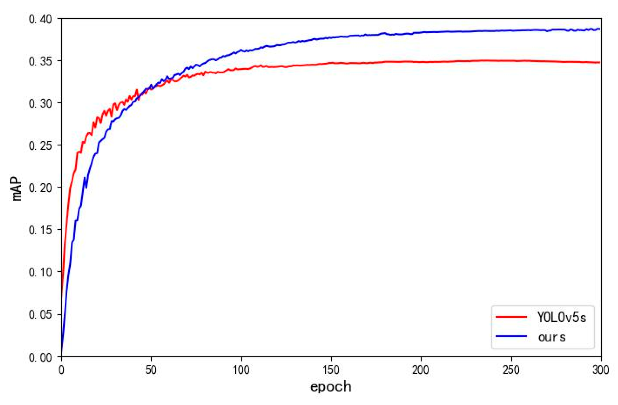
| Method | mAP | FLOPs | Parameters |
|---|---|---|---|
| YOLOv5s | 0.35 | 16.0G | 7.0M |
| Ours | 0.387 | 10.6G | 1.3M |
| Improve | +3.7% | -5.4G | -81.4% |
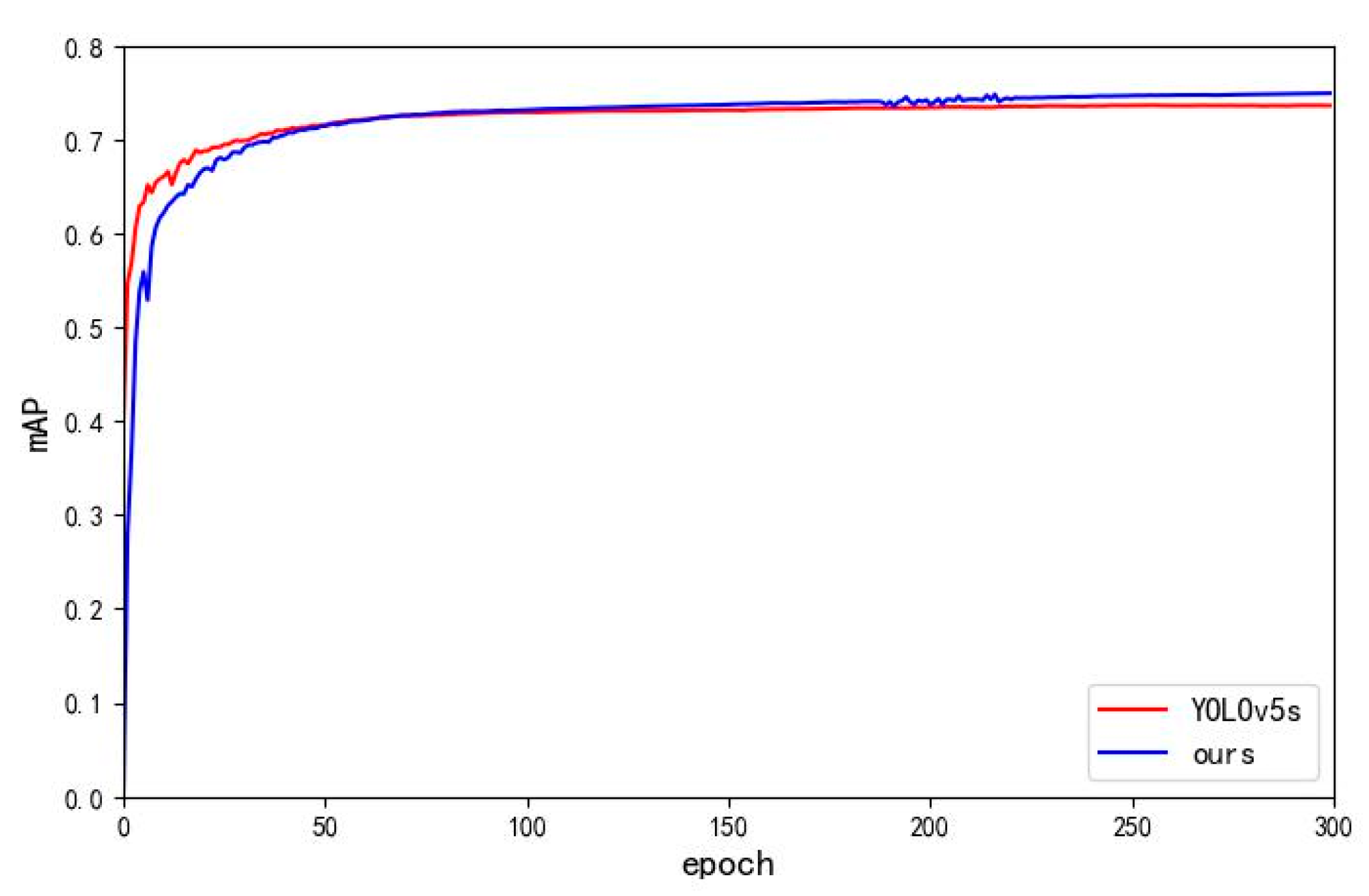
| Method | mAP | FLOPs | Parameters |
|---|---|---|---|
| YOLOv5s | 0.736 | 16.0G | 7.0M |
| Ours | 0.75 | 10.6G | 1.3M |
| Improve | +1.4% | -5.4G | -81.4% |
Disclaimer/Publisher’s Note: The statements, opinions and data contained in all publications are solely those of the individual author(s) and contributor(s) and not of MDPI and/or the editor(s). MDPI and/or the editor(s) disclaim responsibility for any injury to people or property resulting from any ideas, methods, instructions or products referred to in the content. |
© 2024 by the authors. Licensee MDPI, Basel, Switzerland. This article is an open access article distributed under the terms and conditions of the Creative Commons Attribution (CC BY) license (http://creativecommons.org/licenses/by/4.0/).


