1. Introduction
Over the past seven decades, substantial efforts have been made to develop optical computers for real-time data processing owing to their potential advantages in terms of speed and parallelism over electronic computers [
1,
2,
3]. Notwithstanding these efforts, optical computing has failed to outpace digital computing, which has advanced more rapidly and offers greater power, ease of use, and flexibility [
4]. Optical computing remains predominantly analog, while electronic computing is digital. This fundamental difference has posed challenges, as digital optics lack the necessary components to compete directly with electronics. By contrast, free-space optics [
3] and smart pixels [
5,
6] represent promising solutions for overcoming the limitations of electronic processors, particularly in artificial neural networks [
7]. Purely electrical neural networks face a complex topology of connections as the number of input and output nodes increases, which can cause significant electromagnetic crosstalk or noise, specifically at high clock rates [
3,
4]. However, light paths in free-space optics can cross without electromagnetic crosstalk, simplifying interconnections and reducing fabrication costs. This feature is particularly advantageous in neural networks, which are inherently analog and tolerant to some input errors [
7]. Consequently, researchers have proposed a hybrid approach, combining optics and electronics, leveraging optics for tasks where it excels [
1].
Extensive research has been conducted on optical neural networks (ONNs); however, their complexity and bulkiness have hampered their commercial success compared to digital electronics [
1,
2,
8,
9,
10,
11,
12,
13,
14]. To simplify the system and reduce optical crosstalk while maintaining immense optical parallelism from free-space optics, ONNs based on Köhler illumination using lens arrays and a spatial light modulator have been suggested, and their performances have been analyzed [
15,
16,
17]. In these types of systems, optics have been used for linear calculations, while smart pixels or electronics have been employed for nonlinear calculations. Furthermore, this architecture has evolved into a bidirectional ONN (BONN) to handle backward data flow, such as the backpropagation algorithm [
17]. The capability of sending data in the backward direction also enables a two-mirror-like BONN (TMLBONN), which emulates multilayer calculations, saving considerable hardware space. However, for the successful implementation of the backpropagation algorithm in a BONN, it is essential to develop a fast spatial light modulator (SLM) capable of handling frequent changes in data flow. The change in data flow demands the updating of weights in each layer at a fast rate, exceeding several hundred megahertz. Nevertheless, most currently available SLMs are slow and only serially addressable, resulting in considerable latency [
18,
19]. Despite recent advancements in microelectromechanical systems (MEMS) technology, most SLMs still operate in the range of tens of kilohertz, which is significantly slower than electronic switches. Therefore, the slow speed of currently available SLMs causes considerable latency within the BONN architecture. To address these issues, we propose an ONN based on free-space optics that uses lens arrays and a smart pixel light modulator (SPLM). The ONNs proposed herein are a variation of the ONNs previously reported, known as a linear combination optical engine (LCOE) [
15] and BONN [
17]. We replace the SLM in the previous systems with the SPLM to achieve higher modulation speeds, resulting in a higher refresh rate of weights in the ONN. Furthermore, we investigate the performance of the SPLM-based ONN (SPONN) and examine the effect of memory usage in the SPLM on the scaling of the ONN, without relying on the clustering techniques used in previous systems to increase the number of input and output nodes.
2. Materials and Methods
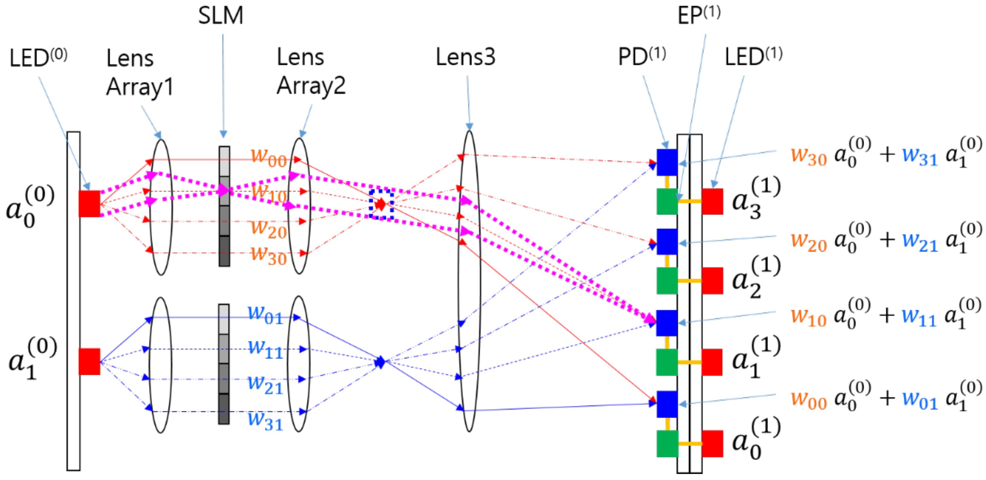
In an ONN based on free-space optics [
15], an SLM is used to represent the weights of the neural network, as shown in
Figure 1. Lens1 distributes the input light into the pixels of the SLM, and Lens2 focuses the rays from the pixels, making the ray slopes different according to the relative position of the pixel from the optical axis of Lens1 and Lens2. Lens3 forms the images of the pixels on the detector plane, collecting rays of equal inclination into the same spot. This Köhler illumination scheme realizes the neural network connection with minimal optical crosstalk between the channels.
Rays from the input nodes pass through Lens1, the SLM, Lens2, and Lens3 until they reach the photodiode (PD). This optical process performs the linear calculations of the neural network in a single step, increasing throughput considerably. If the numbers of input and output nodes constitute two-dimensional N × N and M × M arrays, respectively, then the total number of interconnections is N² × M². The rest of the neural network involves the application of a nonlinear function and sending the result to the next stage, which can be efficiently handled by an electronic processor (EP) as in smart pixels. Because the smart pixels on the detector plane are connected only locally with neighboring pixels, the parallelism of the system is not compromised.
This LCOE architecture shows immense optical parallelism with fixed weights in the neural network, which can be very useful, particularly in inference applications. Although the SLMs are reconfigurable and programmable, the switching speed of currently available SLMs remains at a few kilohertz, which delays calculations and significantly reduces throughput if the weights need to be changed during calculations.
There are two potential solutions for improving the refresh rate of the SLM. The first is to develop a fast SLM array, such as absorption modulators. However, this approach involves significant time, effort, and cost. The second solution is to utilize existing technologies, such as smart pixels, which can integrate the detector, light source, and EP into a chip form. Recently, optoelectronic packaging technologies have advanced significantly, making the hybridization of these devices into an array feasible [
6]. Additionally, the EP can perform various functions with memory, making the ONN more programmable and intelligent compared to using SLMs alone.
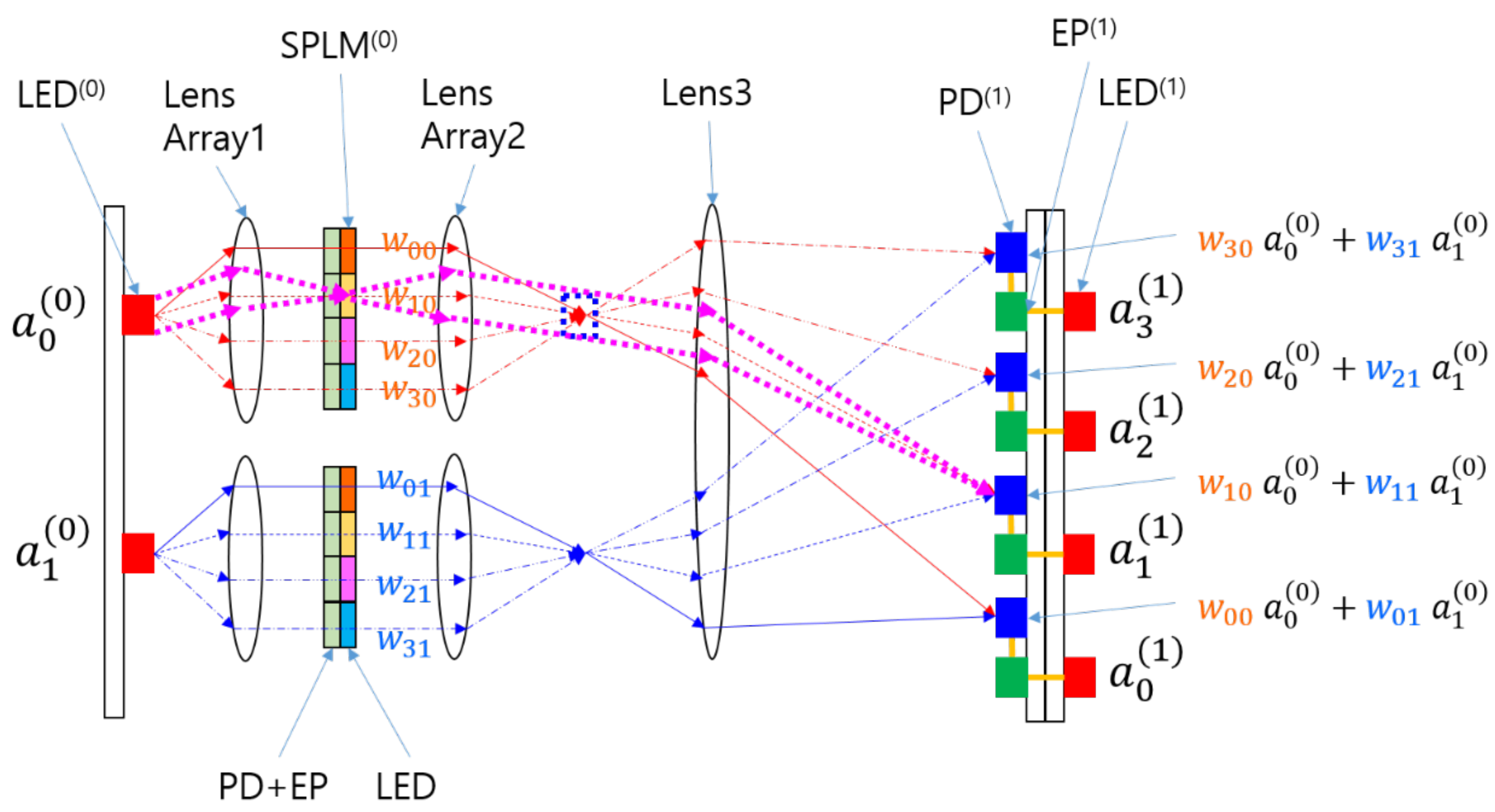
A simple form of the ONN using SPLM is shown in
Figure 2. The SPLM replaces the SLM in the previous LCOE system, while the other parts remain unchanged. The SPLM comprises a PD, an EP, and a light-emitting diode (LED) [
6]. The PD receives the incoming light, converts it into an electrical signal, and sends it to the EP inside the SPLM. The EP amplifies the electrical signal as per the weight value stored in its inherent memory. The output from the EP is sent to the LED, which emits light proportional to the input and weight. The PD, EP, and LED form a pixel, and such pixels are only locally connected except when the program is being downloaded. Once the program is loaded, the array of pixels operates independently, maintaining the parallelism of the system. Each pixel essentially functions as a small repeater.
Because the components are electronic, the modulation speed exceeds several hundred megahertz, which is much higher than that of typical SLMs such as liquid crystal displays (LCDs) and MEMS [
18,
19]. Although the use of SPLM introduces two additional steps of conversion between optical and electronic signals, the delay from this process is less than a few nanoseconds [
6]. However, the gain from the high modulation speed of the SPLM is much greater in many applications, as mentioned in the introduction.
Another difference between the SPONN and the SLM-based ONN is that the LED output of the SPLM changes the divergence of the rays, whereas the SLM maintains collimated light. This issue can be mitigated by using a small lens after the LED. However, this diverging beam does not affect the performance of the ONN because the SLM or SPLM plane is conjugate to the detector plane of the ONN through Lens2 and Lens3. This means the image of the LED in the SPLM forms at the detector plane regardless of the divergence angle of the LED.
The SPONN can be further simplified by replacing LED
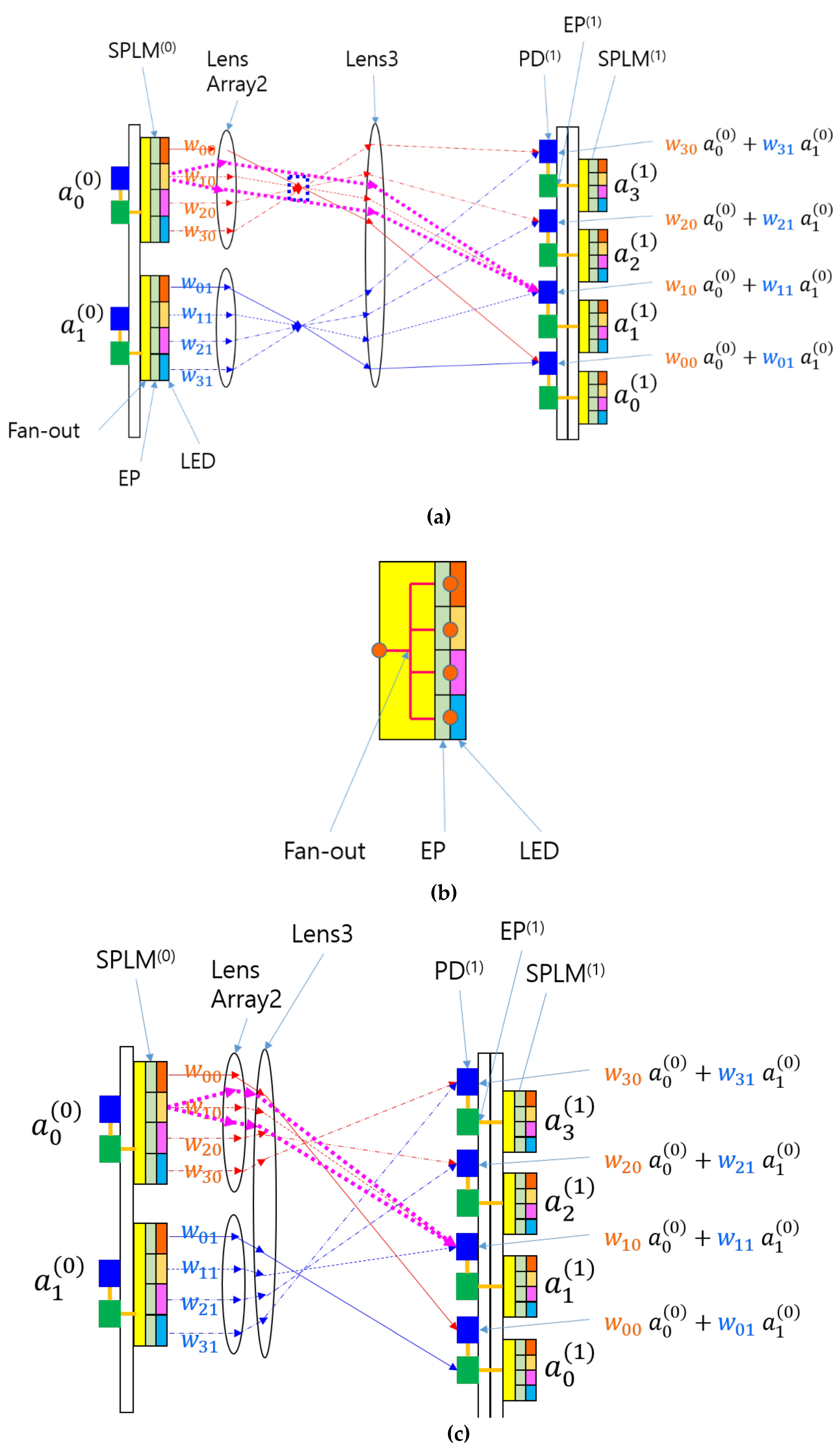
(0) and Lens1 with an electrical fan-out, as shown in
Figure 3(a). The electrical fan-out is illustrated in detail in
Figure 3(b). The light input and Lens1 function as an optical distributor of the input signal, while the electrical fan-out in
Figure 3(a) and 3(b) serves as an electrical distributor. This electrical distributor has a simple wiring topology that connects the output of the preceding layer to the inputs of the pixels in the following SPLM. This simple topology reduces wiring complexity and electromagnetic noise. By using an electrical fan-out, the number of components and the burden of optical alignment can be reduced, thereby simplifying the system.
The removal of LED
(0) and Lens1 simplifies the optics and eliminates the need for Köhler illumination, in which Lens1 and Lens2 form a condenser system and Lens2 and Lens3 form a projection system. With only the projection system remaining, further simplification is possible, as shown in
Figure 3(c). In this configuration, the distance between Lens2 and Lens3 can be shortened, or they can be combined into a single lens using cementing or a diffractive optical element. Combining them into one element saves space and reduces the burden of optical alignment, leading to cost reduction. Each layer of the system comprises an input smart-pixel array, a lens array, and an output detector array with a smart-pixel array.
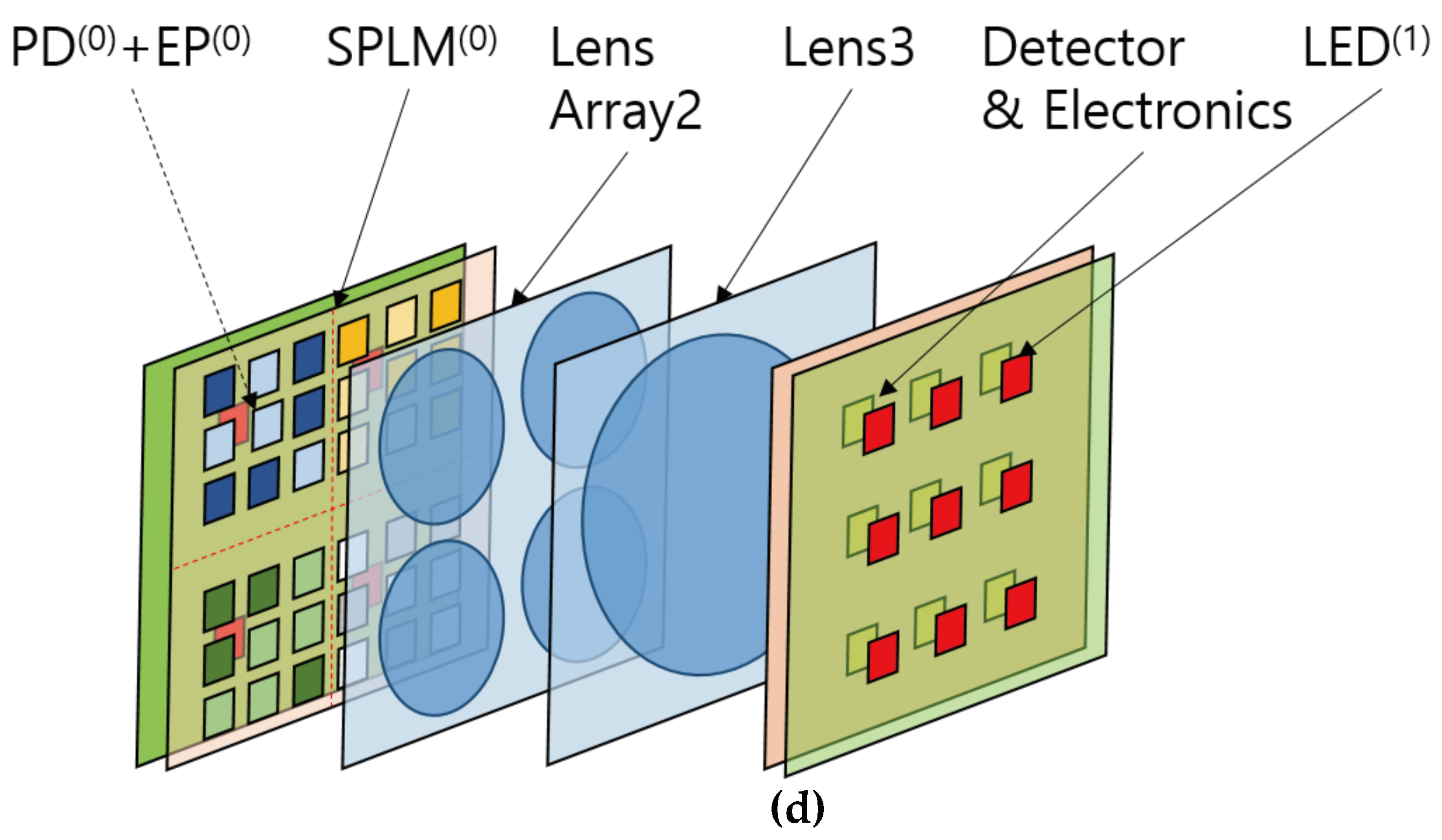
Overall, the replacement of SLM by SPLM greatly simplifies the system and may reduce fabrication difficulty and cost in the future. A three-dimensional view of the SPONN is shown in
Figure 3(d). This architecture is cascadable and accommodates multilayer ONNs like the LCOE.
3. Results
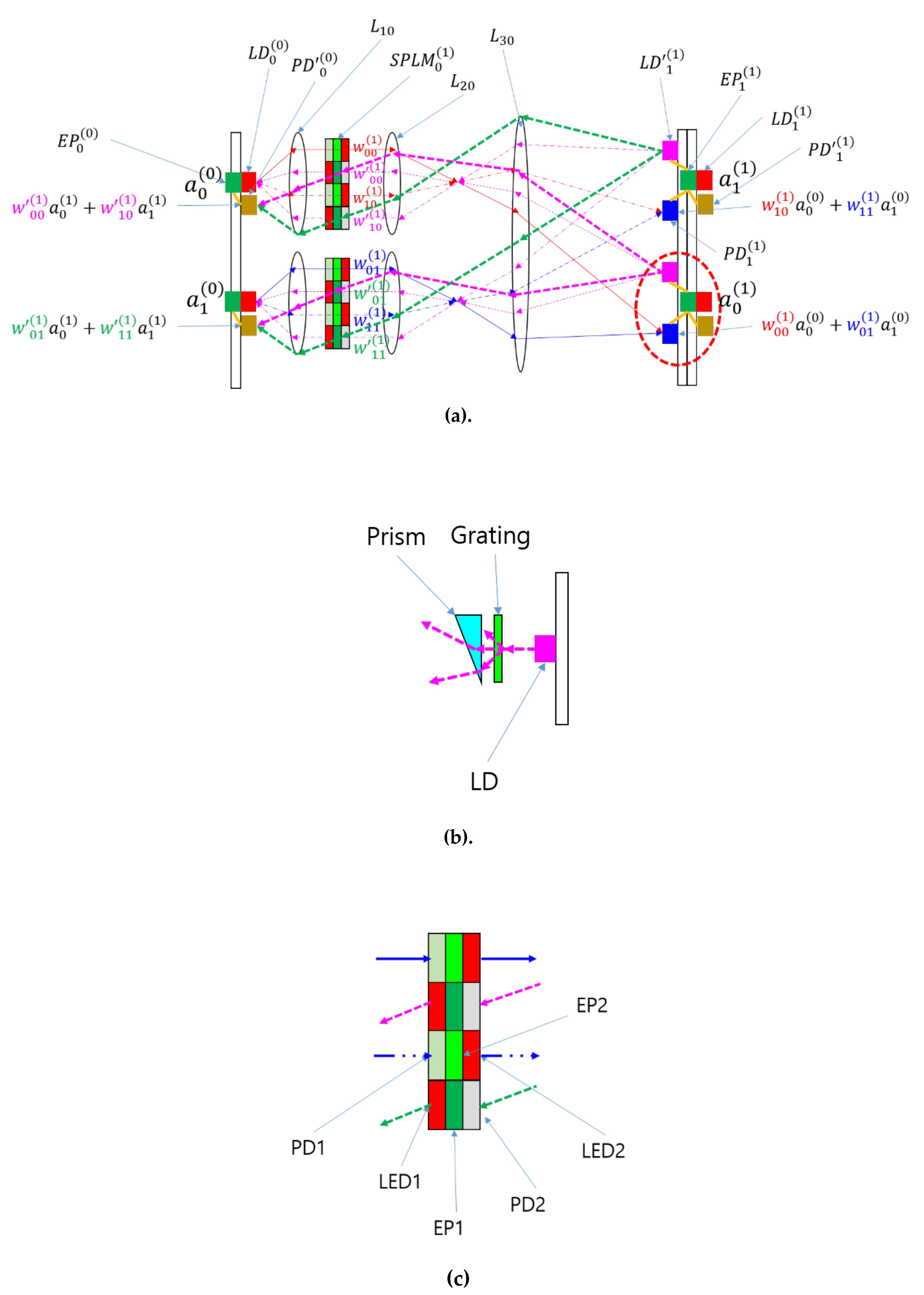
The application of SPLM in an ONN can also be extended to BONN, as illustrated in
Figure 4(a). In the SPLM-based BONN (SPBONN) architecture, the SPLM replaces the SLM, which was previously responsible for modulating light propagating in both forward and backward directions according to the weight values of the neural network [
17]. The images of the SPLM pixels are formed on the detectors in the second substrate or the detector plane using Lens2 (
L20) and Lens3 (
L30). The second substrate also includes light sources (
) for backward propagation, as shown in
Figure 4(b). The light source for the backward direction can include a laser diode, grating, and prism to control the properties of the output beams, which pass through the SPLM and focus on the PDs (
) on the first substrate for the backward direction. This entire BONN scheme is preserved even after replacing the SLM with SPLM, with the key improvement being a dramatic increase in modulation speed.
Because the SPLM can modulate light at several hundred megahertz, the refresh rate of the weights of the neural network can also reach a few hundred megahertz, as the next weight stored in the EP memory is sent to the amplifier within a few nanoseconds. This high refresh rate eliminates most of the concerns associated with the slow modulation of SLM in the previous BONN architecture. Replacing the SLM with SPLM enables the practical implementation of the backpropagation algorithm and the TMLBONN structure without the need for developing new types of fast SLM array devices.
The SPLM used in this BONN differs from those in
Figure 2 and
Figure 3; the details are shown in
Figure 4(c). To enable bidirectional modulation, the pixels are divided into two groups. One group is dedicated to the forward direction, featuring PD1 on the left side and LED2 on the right side of the same pixel, connected via EP2. The other group is designed for the backward direction, with PD2, EP1, and LED1 within a pixel to modulate light in reverse. LED1 may include a microprism or lens to control emission and divergence angles.
As with the simplification from
Figure 2 to
Figure 3, a similar approach can be applied to transform the SPONN in
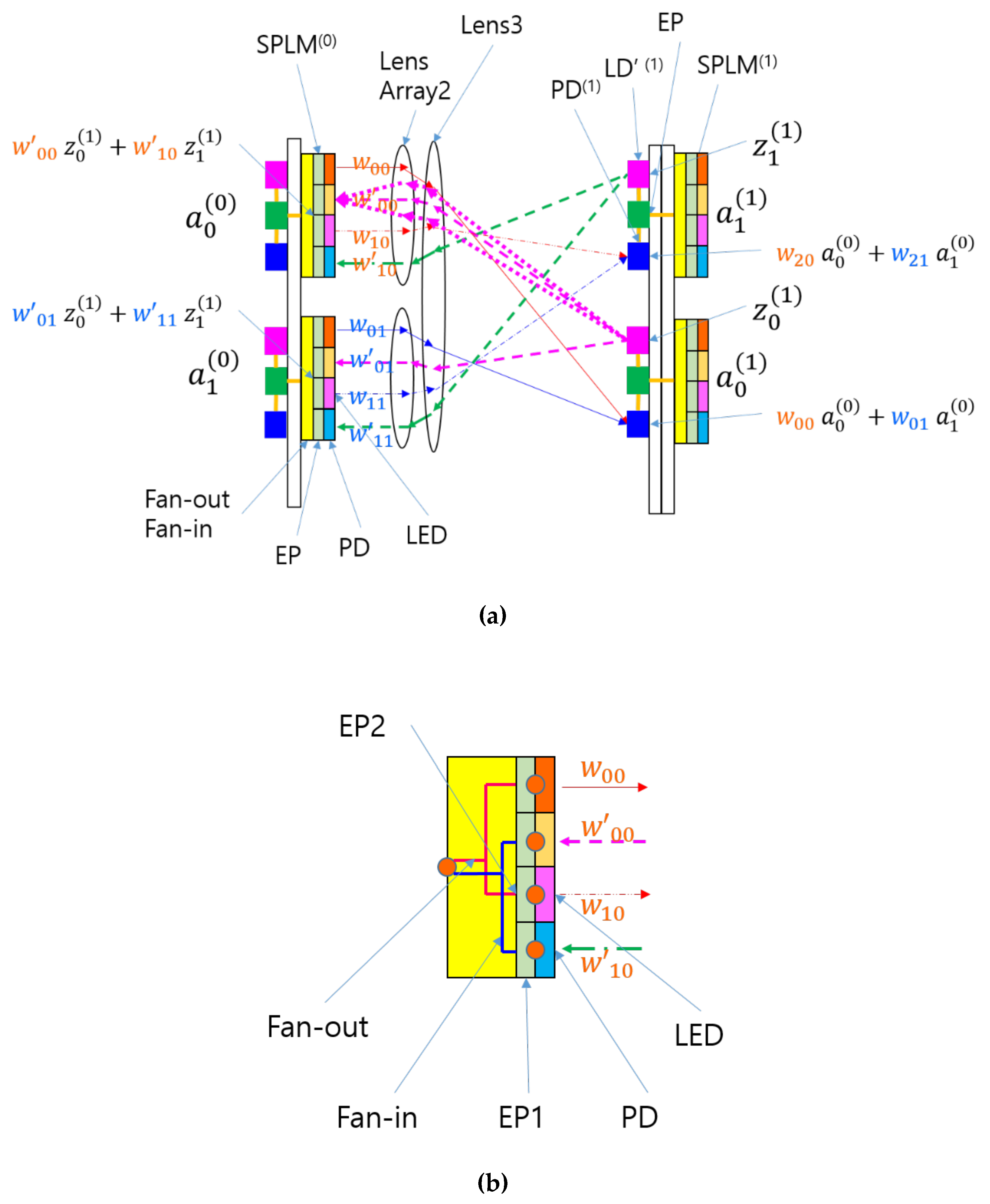
Figure 4 into that in
Figure 5 by using electrical fan-in and electrical fan-out to replace the optical input distribution previously achieved with Lens1. The final SPBONN design comprises SPLM, lenses, and smart pixels on the second substrate, maintaining the same bidirectional data flow while significantly simplifying the hardware structure. The electrical fan-in is introduced to perform the analog summing of optical signals for the backward direction, as in the previous version of the BONN. The EPs within the SPLM convert the output into current, and the electrical fan-in aggregates this current into the electrical input/output node of the EPs in the preceding layer.
To assess the SPBONN, it is important to understand the scalability of the BONN system, which is inherited from the LCOE [
15,
17]. The core of the SPBONN lies in its projection system, comprising Lens2 and Lens3 as shown in
Figure 5. This system faces scalability limitations if clustering techniques are not employed [
15,
17]. Geometrical aberrations and image magnification restrict the size of the input and output arrays to less than 192 × 192 if the worst-case angular aberration is 1 mrad and the f-number (f/#) of Lens2 is 2, respectively. Each bidirectional channel requires four subchannels to manage forward and backward data flow in the difference mode. Consequently, the maximum input or output array size is limited to 96 × 96 under the optical constraints outlined in reference [
14]. This array size enables approximately (96 × 96)², or 8.5 × 10⁷, parallel multiply-and-accumulate (MAC) operations per instruction cycle. Assuming a delay of approximately 10 ns in the SPLM and an additional 10-ns delay in the detector plane of the second substrate, the parallel throughput of a single layer is estimated to be 4.3 × 10¹⁵ MAC/s. This throughput can be further increased as the number of layers increases, provided the data flow remains continuous, as in inference applications, similar to pipelining in a digital computer, with multiple layers operating simultaneously. For example, if there are 100 layers, the throughput could reach 4.3 × 10¹⁷ MAC/s, surpassing the throughput of a tensor processing unit by nearly 1000 times [
20].
The above estimation does not apply to the backpropagation algorithm, as the data flow during backpropagation occurs in a single pass after the forward calculation. In this scenario, calculations are performed one layer at a time, which means that multiple layers are not activated simultaneously, thereby offering no gain from using multiple layers. In the LCOE architecture, multiple layers are necessary for maintaining high optical parallelism because the refresh rate of weights or the SLM is only a few kilohertz. However, SPBONN does not require multiple layers, which would not only demand significant hardware space but also involve substantial fabrication and assembly efforts, leading to high costs. The SPLM-based TMLBONN architecture addresses this issue by effectively handling the multilayer sequential algorithm, thereby conserving hardware resources. The data flow bouncing between two layers can emulate a multilayer ONN because the weight refresh takes only 10 ns, which can occur during the calculation on the detector plane in the preceding layer. Consequently, there is no additional delay due to weight updates for the next layer.
4. Discussions
The energy consumption of SPBONN needs to be evaluated, as SPLMs may consume more power than SLMs. SLMs, such as LCDs, are highly energy-efficient devices that only rotate liquid crystals using an electric field without generating significant heat. However, SPLMs contain light sources such as LEDs or LDs, which emit light and can generate heat, particularly in large arrays. For example, if each SPLM output pixel in
Figure 5(b) uses a micro-LED measuring 5 × 5 µm² and consuming approximately 1 µW—with a typical current density of 1 A/cm² [
21] and an optical output power of around 0.25 µW—a 96 × 96 input and output array would require 2 × (96 × 96)² LEDs in the SPLM array. The total electrical power consumption would be approximately 170 W. This amount of heat could be dissipated via natural or forced convection without significantly increasing the device temperature, provided the board or substrate, including the light sources, is not excessively small. If the SPLM pixels are spaced 20-μm apart, the total size of the SPLM array would be 370 × 370 mm², which may be large enough for effective heat dissipation using convection alone.
Replacing the SLM with the SPLM enhances the functionality of the ONN, as each smart pixel contains an EP that is programmable and has memory for storing weight data. This memory can be used to scale the number of input and output nodes with some time delay. Previously, the scaling limits of ONNs were overcome by using clustering techniques in hardware, where multiple ONN modules were stacked in layers to redistribute extended input data and make full connections between the doubled input and output nodes [
15]. However, SPONN eliminates the need for hardware scaling by using memory to increase the number of input and output nodes.
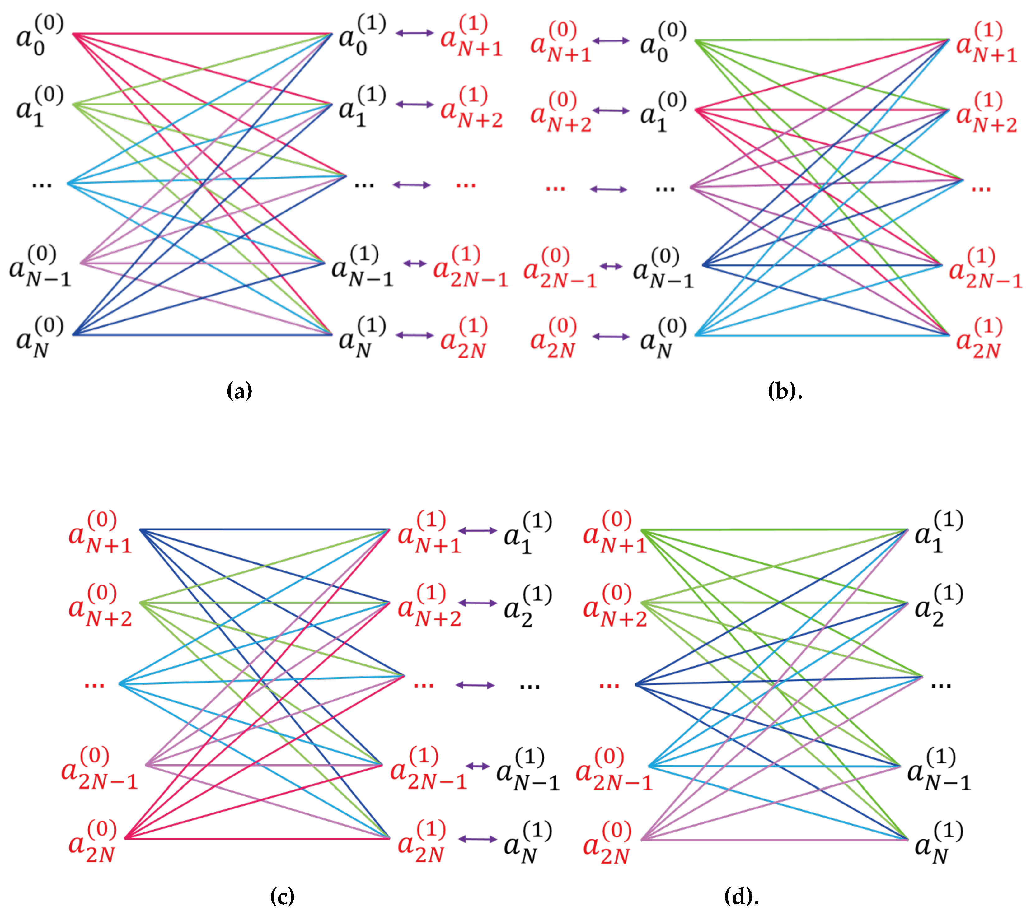
The process of doubling the input and output nodes is illustrated in
Figure 6. First, the full connection between the first batch of N input nodes and the first batch of N output nodes is made, with the output nodes storing the first output batch in memory, as shown in
Figure 6(a). Next, the first input batch is connected to the second batch of N output nodes, and the first input batch is swapped with the second input batch using the memory of the input smart pixels, as shown in
Figure 6(b). Then, the second input batch is fully connected with the second output batch, as depicted in
Figure 6(c). Because the second output batch accumulates all the weighted outputs from both first and second input batches, it is stored in memory and swapped with the first output batch, as shown in
Figure 6(c). Finally, the second input batch is fully connected to the first output batch to complete the first output batch, as shown in
Figure 6(d), which now contains the weighted outputs from both first and second input batches.
This method of doubling input and output nodes can be repeated to further increase the number of nodes. The entire doubling process requires nine steps, which introduces some calculation delays and reduces throughput; however, it provides a way to expand the number of input and output nodes without additional hardware scaling. This approach saves on cost and space, offering flexibility for ONNs to accommodate various input and output sizes.
Smart pixel memory in SPONN can also be used to perform ONN operations in difference mode. In the LCOE configuration, handling negative weights requires an additional optical channel to obtain the weighted outputs and subtract them from the outputs of positive weights. However, in SPONN, inputs are first connected to the positive weights, and the weighted outputs are stored in the smart pixel memory on the second substrate. The positive weights are then replaced with negative weights, and the outputs are recalculated. The negative weighted outputs are subtracted from the positive ones stored in memory. Although this process introduces a slight delay owing to the additional steps, it requires only half the input and output nodes compared to the traditional difference mode. Thus, SPONN can emulate the difference mode using smart pixel memory, with a minimal delay when sufficient input and output nodes are unavailable. This approach is practical because the fast weight-refresh rate of the SPLM significantly reduces the impact of the delay.
5. Conclusions
We investigate the integration of SPLMs into ONNs and BONNs and their advantages over traditional SLMs. SPLMs replace SLMs in these architectures, enabling faster modulation of light in both forward and backward directions. This significant improvement in the refresh rate of the neural network weights to several hundred megahertz is crucial for the practical implementation of the backpropagation algorithm and the TMLBONN structure, eliminating the need for new fast SLM array devices.
The SPLM used in BONN differs from those in SPONN by enabling bidirectional modulation, where pixels are divided into two groups dedicated to forward and backward light propagation. This division allows for effective modulation in both directions, contributing to the overall efficiency and performance of the BONN system. The introduction of electrical fan-in and fan-out in the SPBONN designs further simplifies the hardware structure while maintaining bidirectional data flow.
Scalability is a critical aspect of the SPBONN architecture. The core of SPBONN lies in its projection system, which faces scalability limitations due to geometrical aberrations and image magnification. These constraints limit the input and output array size to 96 × 96, enabling approximately 8.5 × 10⁷ parallel MAC operations per instruction cycle. Despite these limitations, the parallel throughput of a single layer can reach 4.3 × 10¹⁵ MAC/s, which can be further increased with additional layers, similar to pipelining in digital computers. For instance, with 100 layers, the throughput could reach 4.3 × 10¹⁷ MAC/s. The increase in throughput by using multiple layers does not apply to the backpropagation algorithm, where calculations are performed one layer at a time. Because multiple layers are not activated simultaneously, the need for high optical parallelism across multiple layers is reduced, along with the hardware space requirements. The SPLM-based TMLBONN architecture addresses these challenges by effectively managing multilayer sequential algorithms with high weight-refresh rates, conserving hardware resources, and ensuring efficient data flow between layers.
An assessment of the energy consumption of SPBONN was conducted, given that SPLMs may consume more power than SLMs. Unlike SLMs, such as LCDs, which are energy efficient and produce minimal heat, SPLMs use LEDs or LDs that emit both light and heat, particularly in large arrays. For instance, a 96 × 96 SPLM array could consume approximately 170 W. However, effective heat dissipation via convection is feasible if the SPLM array is sufficiently large.
Replacing SLMs with smart pixels in the ONN enhances its functionality, as each smart pixel contains an EP with programmable memory to store weight data. This memory facilitates the scaling of the number of input and output nodes without additional hardware, overcoming previous scaling limitations that required clustering techniques and hardware stacking. The method of doubling input and output nodes using smart pixel memory offers a flexible and cost-effective way to expand the neural network without hardware scaling, although it introduces some calculation delays and reduces throughput.
In summary, replacing SLM with SPLM in ONN significantly boosts the weight refresh rate, making BONN and TMLBONN highly practical for achieving massive parallelism and rapid reconfigurability with current smart-pixel technologies. Additionally, incorporating memory within smart pixels overcomes scaling limitations, providing flexibility to accommodate various input and output node sizes. These advancements suggest that the newly proposed architectures could pave the way for more general-purpose optical computing in the future.
Funding
This research received no external funding.
Data Availability Statement
The datasets generated during and/or analyzed during the current study are available from the corresponding author on reasonable request.
Conflicts of Interest
The authors declare no conflict of interest.
References
- Ambs P.: Optical Computing: A 60-Year Adventure Advances in Optical Technologies 2010 1-15 (2010). (DOI:10.1155/2010/372652, hal-00828108).
- McAulay, A.D.: Optical Computer Architectures (Wiley-Interscience, USA) (1991).
- Jahns, J., Free-Space Optical Digital Computing and Interconnection, in: Progress in Optics, E. Wolf (ed.), Elsevier, vol. 38, pp. 419-513 (1998).
- Streibl N., Brenner K.H., Huang A., Jahns, J., Jewell, J., Lohmann, A. W., Prise, M. E., and Sizer, T., Miller, D.A.B. and Murdocca, M.: Digital Opitcs, 1989 Proceedings of the IEEE 77 1954-1969 (1989).
- Seitz, P. Smart Pixels, PROCEEDINGS EDMO 2001 / VIENNA, 229-234 (2001).
- Hinton, H.S., 1996. Progress in the smart pixel technologies. IEEE journal of selected topics in quantum electronics, 2(1), pp.14-23.
- Rosenblatt, F. The Perceptron: A Probalistic Model For Information Storage And Organization In The Brain Psychological Review 65 386–408. CiteSeerX 10.1.1.588.3775. PMID 13602029 (1958). [CrossRef]
- Khonina, S.N.; Kazanskiy, N.L.; Skidanov, R.V.; Butt, M.A. Exploring Types of Photonic Neural Networks for Imaging and Computing—A Review Nanomaterials, 2024, 14, 697. [CrossRef]
- Liao, K.; Dai, T.; Yan, Q.; Hu, X.; Gong, Q. Integrated Photonic Neural Networks: Opportunities and Challenges. ACS Pho-tonics 2023 10 (7), 2001-2010. [CrossRef]
- Caulfield, H.J.; Kinser, J.; Rogers, S.K. Optical neural networks, Proceedings of the IEEE, vol. 77, no. 10, pp. 1573-1583 (1989).
- Jang, J.S.; Jung, S.W.; Lee, S.Y.; Shin, S.Y. Optical implementation of the Hopfield model for two-dimensional associative memory, Optical Letters, 1988, 13, 248-250. [CrossRef]
- Zhou, T.; Lin, X.; Wu, J.; Chen, Y.; Xie, H.; Li, Y.; Fan, J.; Wu, H.; Fang, L.; Dai, D. Large-scale neuromorphic optoelectronic computing with a reconfigurable diffractive processing unit, Nature Photonics, 2021, 15, 367–373. [CrossRef]
- Liu, J.; Wu, Q.; Sui, X.; Chen, Q.; Gu, G.; Wang, L.; Li, S. Research progress in optical neural networks: theory, applications and developments, PhotoniX, 2021, 2:5. [CrossRef]
- Lin, X.; Rivenson, Y.; Yardimci, N. T.; Veli, M.; Luo, Y.; Jarrahi, M.; Ozcan, A. All-optical machine learning using diffractive deep neural networks. Science, 2018, 361(6406), 1004-1008. [CrossRef]
- Ju, Y.G. A scalable optical computer based on free-space optics using lens arrays and a spatial light modulator. Optical and Quantum Electronics, 2023, 55(3), p.220. [CrossRef]
- Ju, Y.G. Scalable Optical Convolutional Neural Networks Based on Free-Space Optics Using Lens Arrays and a Spatial Light Modulator. Journal of Imaging, 2023, 9(11), p.241. [CrossRef]
- Ju, Y.-G. Bidirectional Optical Neural Networks Based on Free-Space Optics Using Lens Arrays and Spatial Light Modulator. Micromachines 2024, 15, 701. [CrossRef]
- Cox, M.A.; Cheng, L.; Forbes, A. Digital micro-mirror devices for laser beam shaping, Proc. SPIE 11043, Fifth Conference on Sensors, MEMS, and Electro-Optic Systems, 110430Y (2019).
- Mihara, K.; Hanatani, K.; Ishida, T.; Komaki, K.; Takayama, R. High Driving Frequency (> 54 kHz) and Wide Scanning An-gle (> 100 Degrees) MEMS Mirror Applying Secondary Resonance For 2K Resolution AR/MR Glasses. 2022 IEEE 35th Inter-national Conference on Micro Electro Mechanical Systems Conference (MEMS), 477-482 (2022).
- Tensor Processing Unit. Available online: https://en.wikipedia.org/wiki/Tensor_Processing_Unit (accessed on 13 August 2024).
- Singh, C.P. and Ghosh, K. Lower current density driven InGaN/GaN micro-LED with improved quantum efficiency. Optik 2024, 300, p.171664. [CrossRef]
Figure 1.
An example of an ONN based on free-space optics using lens arrays and an SLM. LED, SLM, PD, and EP denote light-emitting diode, spatial light modulator, photodiode, and electronic processor, respectively. indicates the i-th input or output node in the l-th layer. represents the weight connecting the i-th input and the j-th output.
Figure 2.
An example of an ONN based on free-space optics using lens arrays and an SPLM. SPLM(l) represents an SPLM in the l-th layer. Each smart pixel in the SMPL contains a PD, an EP, and an LED to modulate the input light with the weight stored in the memory of the EP.
Figure 2.
An example of an ONN based on free-space optics using lens arrays and an SPLM. SPLM(l) represents an SPLM in the l-th layer. Each smart pixel in the SMPL contains a PD, an EP, and an LED to modulate the input light with the weight stored in the memory of the EP.
Figure 3.
Scalable ONN based on free-space optics using lens arrays and an SPLM with electrical fan-out: (a) Schematic of the ONN; (b) schematic of the electrical fan-out used for the input of the SPLM; (c) combining Lens Array2 and Lens Array3; (d) three-dimensional view of a system with a 2 × 2 input and a 3 × 3 output.
Figure 4.
BONN using lens arrays and an SPLM: (a) A schematic of the SPBONN and the associated mathematical formulas. , and denote the i-th laser diode and photodiode in the l-th layer for the forward direction, respectively, while and represent the i-th laser diode and photodiode in the l-th layer for the backward direction, respectively., , and represent Lens Array1, Lens Array2, and Lens3, respectively. and denote the i-th electronic processor and the SPLM in the l-th layer, respectively; (b) light source for the backward direction; (c) schematic of the smart pixel light modulator used for the BONN.
Figure 5.
BONN based on free-space optics using lens arrays and an SPLM with electrical fan-out and fan-in: (a) Schematic of the SPBONN with electrical fan-out and fan-in; (b) schematic of the electrical fan-out and fan-in used for the input and output of the smart pixel.
Figure 5.
BONN based on free-space optics using lens arrays and an SPLM with electrical fan-out and fan-in: (a) Schematic of the SPBONN with electrical fan-out and fan-in; (b) schematic of the electrical fan-out and fan-in used for the input and output of the smart pixel.
Figure 6.
Scaling the connection between input and output nodes using the memory of the smart pixel in the SPONN: (a) Full connection between the first input batch and first output batch, with a swap between the first and second output batches; (b) full connection between the first input batch and second output batch, with a swap between the first and second input batches; (c) full connection between the second input batch and second output batch, with a swap between the first and second output batches; (d) full connection between the second input batch and the first output batch.
|
Disclaimer/Publisher’s Note: The statements, opinions and data contained in all publications are solely those of the individual author(s) and contributor(s) and not of MDPI and/or the editor(s). MDPI and/or the editor(s) disclaim responsibility for any injury to people or property resulting from any ideas, methods, instructions or products referred to in the content. |
© 2024 by the authors. Licensee MDPI, Basel, Switzerland. This article is an open access article distributed under the terms and conditions of the Creative Commons Attribution (CC BY) license (http://creativecommons.org/licenses/by/4.0/).
