1. Introduction
The modern multiple-gate (MG) MOSFET is superior to planar MOSFET in suppressing the short-channel effects (SCEs) and supporting a higher driving current and packing density. Among the MG transistors, the proposed triple-gate (TG) MOSFET (i.e., FinFET)[
1,
2,
3] with the ultra-thin silicon body and 3D gate oxide coverage can enhance the switching speed and decrease more electrostatic power consumption than the double-gate (DG) MOSFET proposed as the first non-planar MOSFET with the unique volume conduction [
4,
5]. Meanwhile, to further increase the IC packing density to accommodate the future GPU for trillion transistor counts, the 3D IC has converted the conventional lateral CMOS layout into the vertical gate-stacked CFET [
6,
7,
8]. The nanosheet MOSFET [
9,
10,
11] comprising CFET has been recognized as an alternative to FinFET and served as the basic building block for the implementation of the next-generation 3D ULSI. As the device feature size is further reduced toward 3nm/2nm, semiconductor node, the free carriers can directly arrive in the drain side without backscattering due to the feature size being smaller than the mean free path. This implies that the traditional drift-diffusion model (DDM), based on the thermal equilibrium between the free carriers and the lattice, is no longer accurate for developing the model of device behavior. Instead of DDM, the ballistic transport model (BTM) should be applied to model the device. The threshold voltage is one of the essential semiconductor device parameters that must be carefully monitored when the 3D ULSI is evaluated for its electrostatic power consumption to achieve power saving. In this work, a unified threshold voltage model for the ballistic FinFET, Ω-gate MOSFET, and nanosheet transistor is achieved based on the quasi-3D scaling theory, the density of state (DOS), and the Fermia-Dirac distribution function. It is shown that the thin silicon, thin gate oxide, and high work function will alleviate the ballistic effects and resist the threshold voltage degradation. Besides, the nanosheet MOSFET exhibits the largest threshold voltage among the three transistors due to the smallest minimum conduction band edge. As the device height/width is further reduced to bring about 2D/1D DOS for the MG MOSFETs, the threshold voltage will be increased to some extent because the 2D/1D DOS can induce a smaller carrier concentration than the 3D DOS for the transistors.
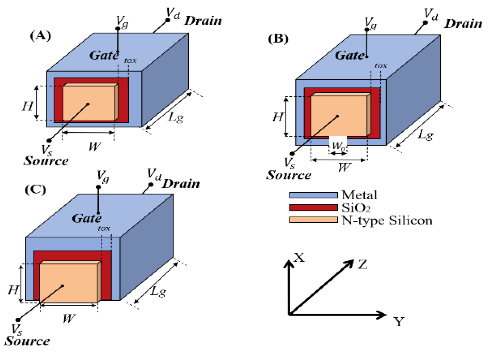
Figure 1.
Typical schematic of the 3D modern multiple-gate MOSFETs composed of (A) nanosheet (NS) MOSFET, (B) W-gate MOSFET, and (C) FinFET. The channel direction is along with the z-axis. The channel length, height, and width are denoted by Lg, H, and W, respectively. The gate oxide thickness is denoted by tox.
2. Model Description
- (A)
Quasi-3D scaling theory for the ballistic MG MOSFETs:
As the device is further scaled down to work in the subthreshold regime, where the electrical field parallel to the channel direction strongly affects the device’s behavior, the channel potential of F
MC can be governed by the quasi-3D scaling theory by accounting for the short-channel effects [
12]:
with
where
fMCL is the long-channel bulk potential. The 3D scaling length l
MG in (1) can be expressed in (2), where l
SG-x—z, l
DG-x-z, and l
DG-y-z are the 2D scaling lengths for the single-gate and double-gate MOSFETs residing in the x-z and y-z cut-plane, respectively.
(
) considers the coupling effects between the x-z and y-z planes and a is the ratio of single-gate oxide to the entire gate oxide in the y-z cut plane. For nanosheet MOSFET, one obtains
=0; for FinFET MOSFET, we have
=1. However, 0<
<1 should be used to develop the 3D scaling length for W-gate MOSFET, W
o is the opening at the bottom gate oxide of W-gate FET. The channel width, height, and gate oxide thickness in (3) are denoted by W, H, and t
ox. The difference in work function between the gate material and silicon body causes the flat-band voltage of V
fb in (4). The solution of (1) can be obtained as
With the boundary conditions of F
MC(z=0)=V
bi, F
MC(Z=L
g)=V
bi+V
ds, the coefficients for T and U in (5) can be obtained as
where V
ds and V
bi are the drain voltage and built-in potential at the junction between the source/drain and channel. With (6) and (7), the minimum channel potential for the ballistic MG MOSFETs can be expressed as
Both T and U in (8) can be linearized for V
gs, which leads to
with
- (B)
Free electron concentration for the ballistic MG MOSFETs:
The free electron concentration for the MG MOSFETs by considering the ballistic transport mode (BTM) can be expressed as:
where g
v is the silicon degeneracy, D(E) is the density of state (DOS), which has been divided by 2 by considering the electron per spin in calculating free electron concentration, f
s(E) and f
d(E) are the Fermin-Dirac distribution function on the source/drain sides, respectively. The 3D DOS in (12), by considering the 3D wave equation, can be obtained as
with
where m
* is the effective mass of the electron and E
C,min is the minimum conduction edge caused by the minimum channel potential of F
min shown in (8). The Fermi-Dirac distribution function on the source/drain sides can be expressed as
with
where E
Fd and E
Fs are the quasi-Fermi levels on the drain/source sides, respectively. By substituting (13), (14), (15), and (16) into (12), the free electron concentration for the ballistic MG MOSFETs can be obtained as
with
and
where
and
are the fermi-Dirac integral of order 1/2. For the non-degenerate carrier statistics (i.e., Maxwell Boltzmann statistics), (17) can be further reduced as
because the Fermi-Dirac integral of any order can be reduced as exponential terms (i.e., F
i(h)=e
h), which is shown as follows:
- (C)
Criterion of threshold voltage for the ballistic MG MOSFETs:
To attain the threshold condition, the minority carrier concentration of n-FET should be equal to the majority carrier concentration of p-FET. This implies that the electron concentration of n in N-FET should be equal to N
a of P-substrate by assuming the complete impurity ionization (i.e., p
N
a) in P-FET. According to the criterion of threshold condition, the threshold voltage of gate bias should satisfy the following criterion:
where V
th is the threshold voltage. By substituting (22) into (20), the minimum channel potential corresponding to the threshold criterion can be obtained as
From (8), (9), (10), (11), and (23), the threshold voltage can be achieved by solving for the quadratic equation of V
gs. This leads to
with
It should be noted that the BTM brings about the new minimum channel potential shown in (23), which can uniquely determine the threshold voltage for the ballistic MG MOSFETs.
- (D)
Free electron concentration for the low-dimensional ballistic MG MOSFETs:
As the device height/weight is shrunk and compatible/smaller than the electron wavelength (~2nm), the 2D/1D DOS should be applied to derive the free electron concentration for the device. The 2D/1D DOS for the MG transistors can be obtained by solving the 2D/1D wave equation. This leads to
D
2D(E) and D
1D(E) have considered the spin per electron. According to the similar developing procedure as shown in (12), the 2D/1D free electron concentration can be expressed as
where F
0(h
F) and F
-1//2(h
F) are the Fermi-Dirac integral of order 0 and -1/2, respectively. They can be expressed as
Similarly, in terms of non-degenerate carrier statistics, (27) and (28) can be further reduced as
Criterion of threshold voltage for the low-dimensional ballistic MG MOSFETs:
By setting free electron density equal to the substrate doping concentration, as shown in (22), the criterion of threshold voltage for 2D and 1D MG devices can be shown as
By replacing Fmin,3D with Fmin,2D, and Fmin,1D, the threshold voltage for 2D and 1D MG MOSFETs can be obtained.
3. Results and Discussion
The 3D device simulator “SDEVICE” is employed to validate the proposed model [
14]. Unless otherwise stated, the following device parameters are used to simulate the MG MOSFETs: the device structure’s square shape, the effective electron mass =1.08m
0, and the valley degeneracy of the silicon g
v=6. The graded density model is included to simulate the carrier density. Also, the quantum-potential model simulates the electrostatic potential, ensuring that the Poisson equation is self-consistent with the wave equation.
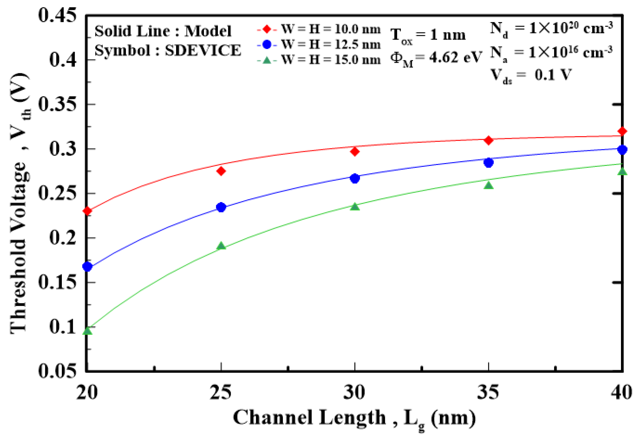
Figure 2 plots the threshold voltage versus the channel length of FinFET for different silicon thicknesses. As the channel length decreases, the thin silicon can produce a larger threshold voltage than the thick silicon due to the alleviated ballistic effects that result in threshold voltage degradation.
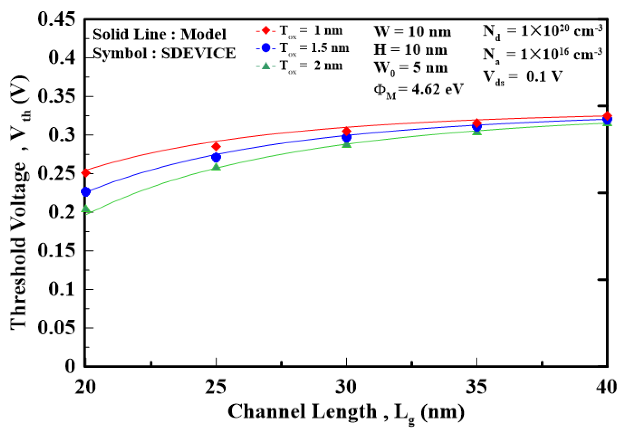
Figure 3 plots the threshold voltage versus the channel length of W-gate MOSFET for different oxide thicknesses. The thin gate oxide that effectively resists the ballistic effects can induce a smaller threshold voltage degradation than the thick gate oxide.
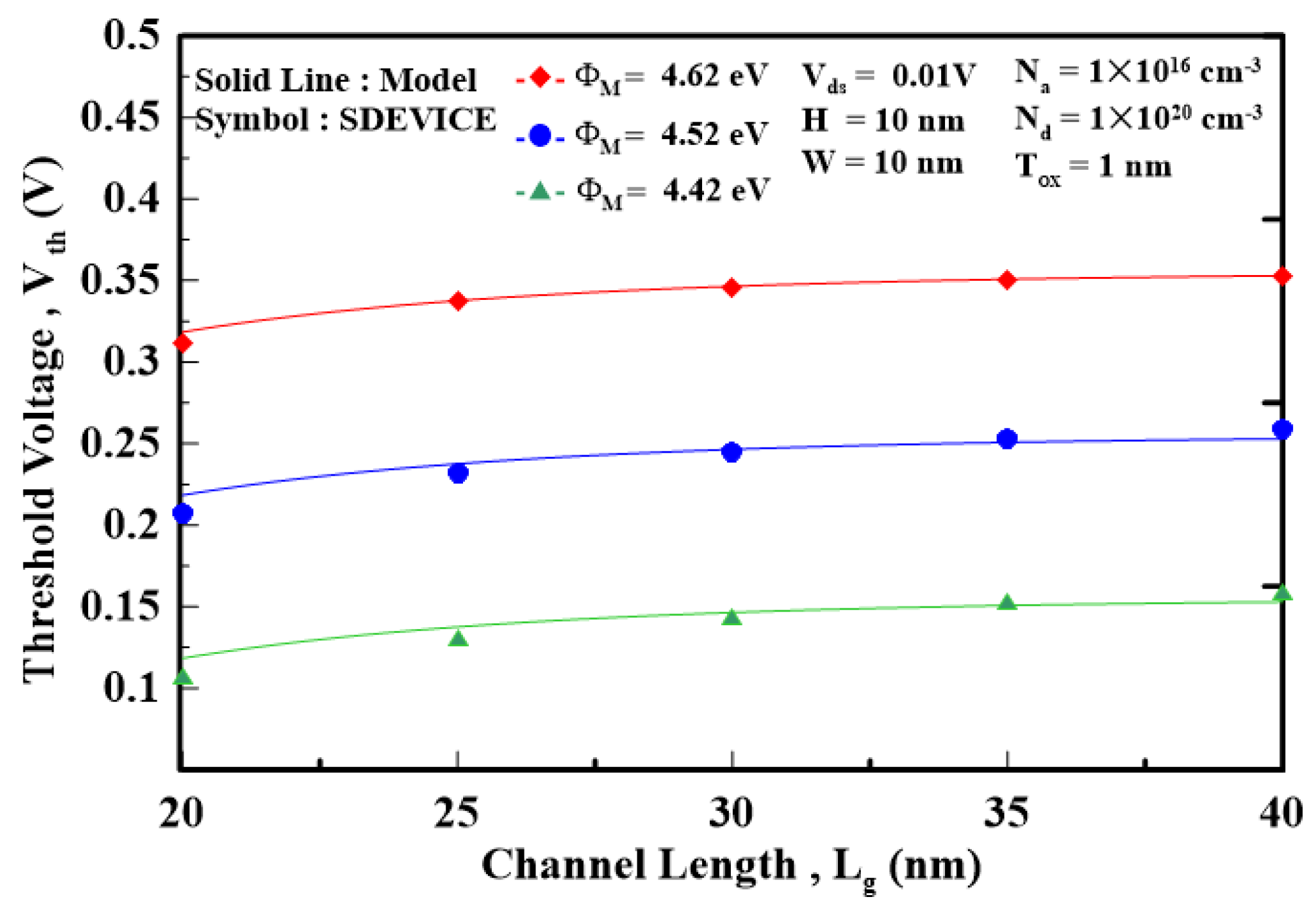
Figure 4 shows how the work function affects the threshold voltage as the channel length is decreased for nanosheet MOSFET. The high work function can bring about a high threshold voltage as the channel length decreases, as opposed to the low work function, which reduces the threshold voltage due to the strong ballistic effects. To show how the different dimensionalities of the devices affect the threshold voltage.
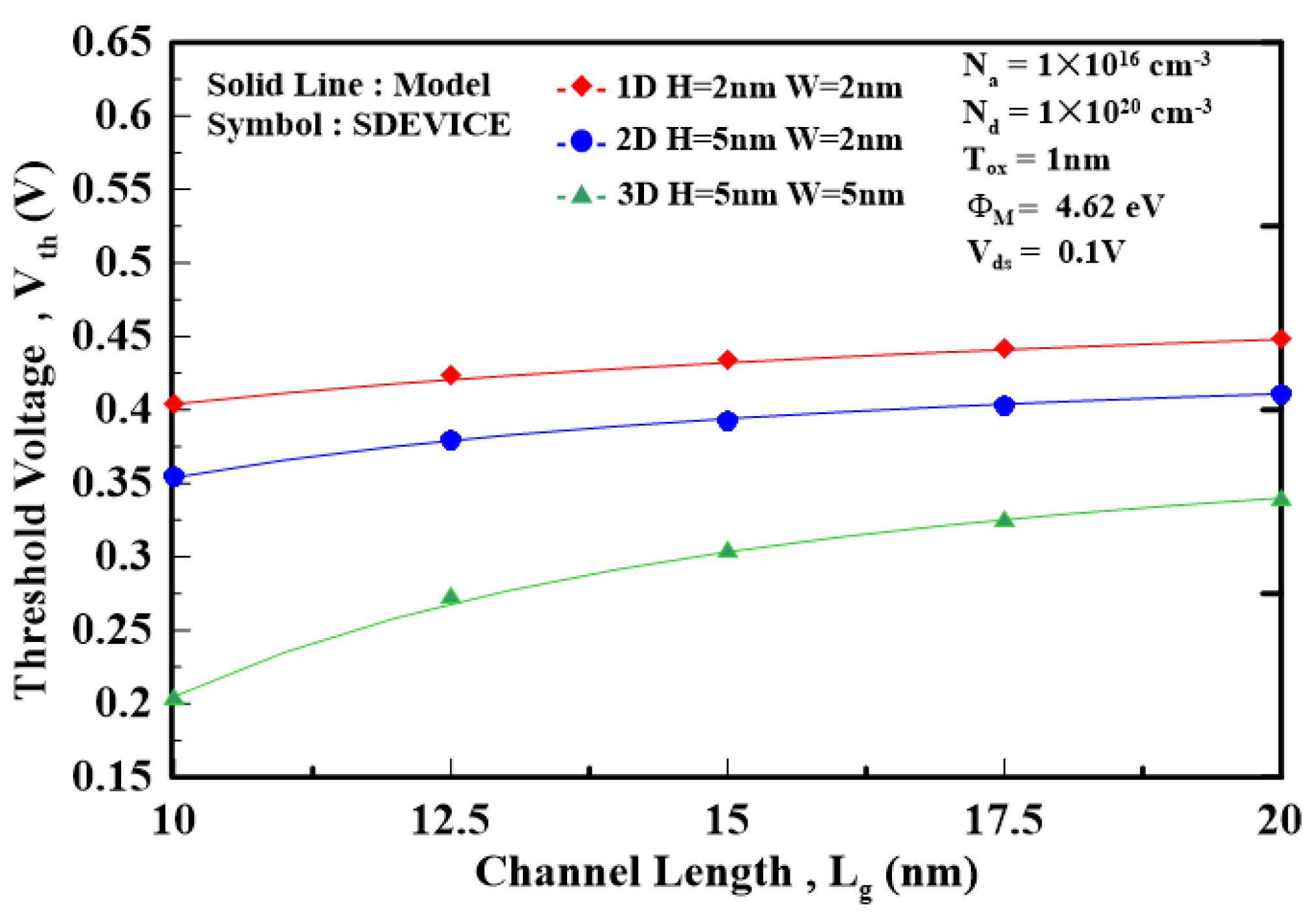
Figure 5 uses the different ratio of device width to device height (i.e., W
H) by considering (2nm
2nm), (2nm
5nm), and (5nm
5nm) cross-section area of FinFET with the channel length decreased from 20nm to 10nm. Note that as the device dimension is approaching the electron wavelength (~2nm), the 2D/1D density of state should be accounted for in calculating the electron concentration, as shown in
Figure 5. It is shown that the 1D device with the cross-section area of 2nm
2nm can induce the largest threshold voltage as opposed to the 3D device with the cross-section area of 5nm
5nm, which results in the smallest threshold voltage because the high-dimensional device cannot effectively alleviate the ballistic effects that degrade the threshold voltage.
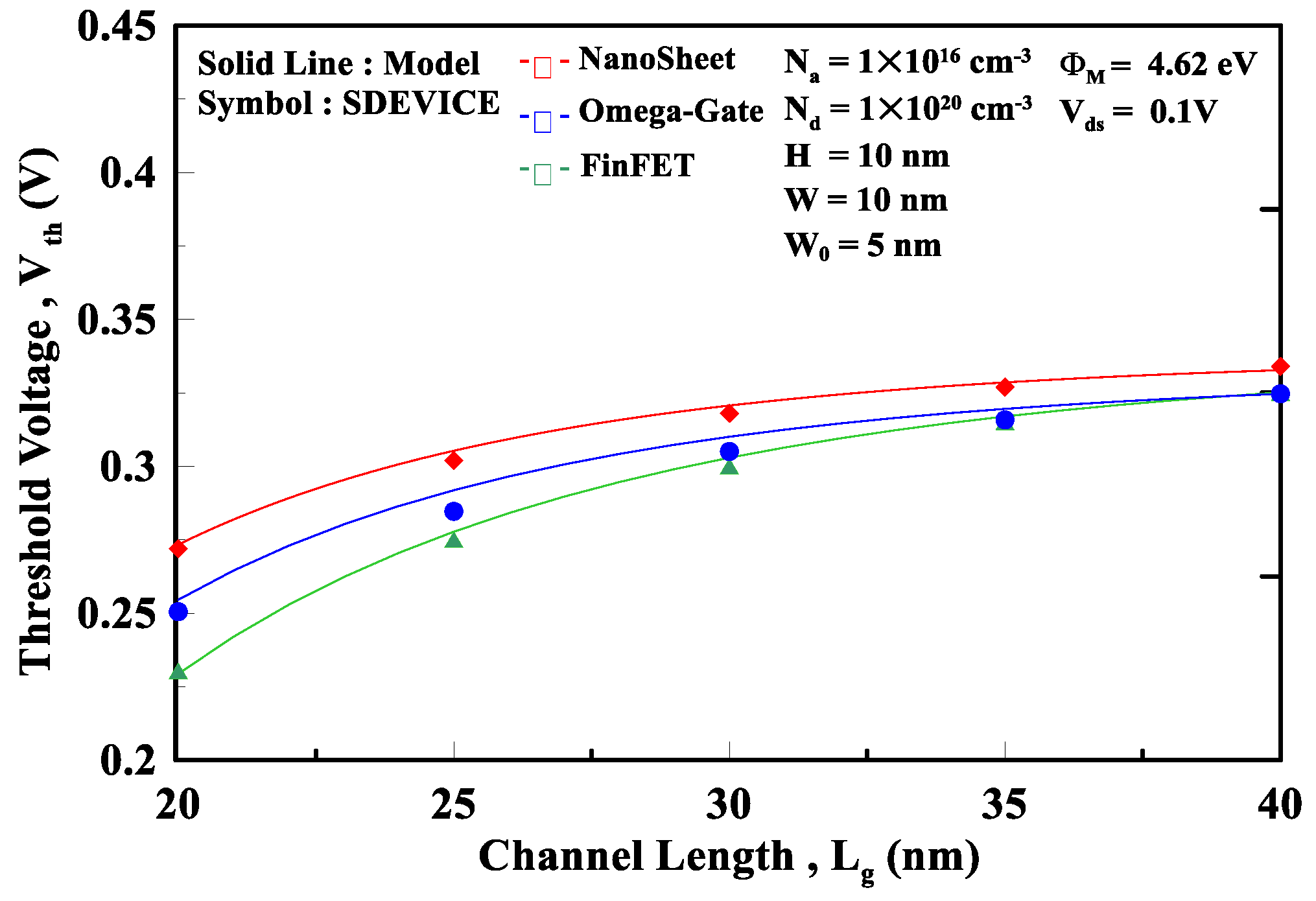
Figure 6 shows the threshold voltage versus the channel length for different devices’ structures, including nanosheet MOSFET. W-gate MOSFET, and FinFET. The nanosheet MOSFET exhibits the largest threshold voltage and smallest threshold voltage degradation with the gate surrounding the channel regime. However, FinFET, with the smallest gate coverage, will show the smallest threshold voltage and largest threshold voltage degradation among the three devices. It is known that the scaling factor can provide the designing guidance for the threshold voltage of the MG devices.
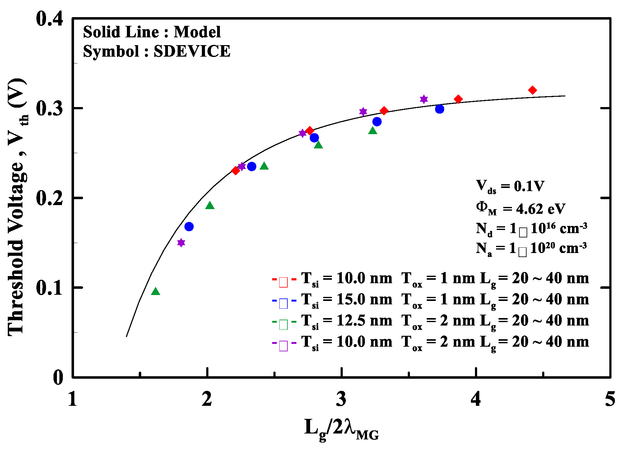
Figure 7 plots the threshold voltage versus the scaling factor for different silicon and oxide combinations of the FinFET. It can be seen that as the scaling factor is reduced below 3, the threshold voltage will be significantly degraded. Therefore, when designing the MG MOSFETs, the allowable silicon/oxide thickness combinations corresponding to the appropriate scaling factor should be carefully accounted for.
