Preprint
Article

3D Light-Direction Sensor Based on Segmented Concentric Nanorings Combined with Deep Learning

Altmetrics

Downloads

60

Views

28

Comments

0

A peer-reviewed article of this preprint also exists.

Submitted:

02 September 2024

Posted:

02 September 2024

You are already at the latest version

Alerts
Abstract
High-precision, ultra-thin angular detectable imaging upon a single pixel holds significant promise for light field detection and reconstruction, thereby catalyzing advancements in machine vision and interaction technology. Traditional light-direction angle sensors relying on optical components like gratings and lenses face inherent constraints from diffraction limits in achieving device miniaturization. Recently, angle sensors via coupled double nanowires have demonstrated prowess in attaining high-precision angle perception of incident light at sub-wavelength device scales, which may herald a novel design paradigm for ultra-compact angle sensors. However, the current approach to measure the three-dimensional (3D) incident light direction is unstable. In this paper, we propose a flexible segmented concentric nanorings structure capable of discerning the 3D light-direction based on its sensitivity character to both elevation (θ) and azimuth (ϕ) angles at a micrometer device scale. Through deep learning (DL) analysis and prediction, our simulations reveal that for angle scanning with a step size of 1o, the device can still achieve a detection range of 0∼360o for azimuth and 45o∼90o for elevation, with an average accuracy of 0.19o, and DL can further solve some data aliasing problems to expand the sensing range. Our design broadens the angle sensing dimension based on mutual resonance coupling among nanorings segments, and through waveguide implementation or sensor array arrangements, the detection range can be flexibly adjusted to accommodate diverse application scenarios.
Keywords: 
Subject: Physical Sciences  -   Optics and Photonics

1. Introduction

The information of the incident angle is crucial for light field detection and reconstruction [1]. Relying on the angle information, wavefront detection, dynamic ranging, and image refocusing can thus be implemented [2,3,4], and these capabilities have significant implications in machine vision, virtual reality (VR), and augmented reality (AR) [5]. The key to design angle sensors lies in converting the incident angle information into other corresponding measurable physical quantities with high angular sensibility. Generally, physical effects with angular sensitivity include light projection and masking, the Talbot effect, and the resonance coupling mechanism [6].
Specifically, light projection and masking refer to the angle detection based on the dependence of projection area on the incident angle of light rays [7,8]. A typical example is the four-quadrant detector (4-QD) [9], which determines the angle of incident light by calculating the proportion of light currents among the four different quadrants. The Talbot effect describes the self-imaging property of periodic objects such as diffraction gratings, and the shifts or the depth of self-images are sensitively changeable by the variation of the angle for incident light. Via this effect, the incident angles can be obtained according to changing rules of the self-images [10]. The perovskite nanocrystals have excellent optoelectronic properties and can produce adjustable emissions with high color saturation under specific spectra, which can convert the light field information into color output. Through arranging the multicolor-emitting perovskite nanocrystals geometrically, the incident light angles can be calculated by decoding the color output, which utilizes the mutual occlusion between the nanocrystals under angular irradiation [11]. As for the resonance coupling, it typically occurs in subwavelength structures or devices such as nanowires and surface plasmon, which describes the interaction of structures under excitation and its characteristics are tightly related to the incentives. Through elaborate design and testing, the resonance can be used for angle detection, which can be deduced by measurable physical quantities, e.g. photocurrents [12,13,14].
However, the above-mentioned incident light angle measurement methods are limited to planar angle measurement and belong to the two-dimensional (2D) level. Comprehensive detection of three-dimensional (3D) light-direction, including the elevation angle ( θ ) and azimuth angle ( ϕ ), typically relies on the combination of sensors, which often entails a compromise between the sensor’s detection ability and physical size. Although the perovskite-nanocrystals-based method is capable of sensing three-dimensional (3D) light-direction, its large-scale application is relatively costly and complex. While, with the design goals of ultra-small, high-precision, and wide-sensing-range, angle-sensors relying on lenses or gratings suffer a sharp decrease in accuracy when their scales approach or are smaller than the wavelength due to the diffraction limitation [15].
To address the challenge of miniaturization on light-direction sensors, inspired by the directional sensing ability of small animals to sound and light waves, angle-sensors based on coupled nanowires have demonstrated high-precision angle perception of incident light at sub-wavelength scales and can be manufactured with existing mature nanofabrication processes [16,17,18,19]. In this work, we propose a 3D light-direction sensor unit based on the angular dependency of the resonant energy distribution within segmented concentric nanorings, capable of detecting incident light-direction upon a single device. Even more, deep learning (DL) method is employed to fit and reason the calculation relationship between the angles and the proposed structural responses, thus the trained data-driven model can be used to obtain angles. Additionally, the fabrication and measurement feasibility of the proposed sensor are shown. In terms of application, the proposed detector can be integrated with devices such as lenses and waveguides to enhance application flexibility and improve detection performance.

2. Materials and Methods

2.1. Nanorings Resonance for Angle Sensing

Paired resonant nanowires with a high refractive index have been theoretically and experimentally demonstrated to exhibit strong angular sensitiveness of leaky-mode resonance, suitable for angle sensors. Similarly, as a commonly used coupled waveguide device, concentric nanorings can couple and resonate with 3D light-direction angular dependence under incident light irradiation [20]. For concentric silicon nanorings shown in Figure 1a, the nanorings with the same width ( w ) and height ( h ) are arranged concentrically with a spacing ( d ), and the radius of the inner nanoring is defined as r .
When space light is incident at elevation angle ( θ ) and azimuth angle ( ϕ ), optical Mie resonances will be supported within the inner and outer nanoring cross-sections a i ( α ) and a o ( α ) determined by the coordinate angle α in cylindrical coordinates ( ρ , α , z ) (Figure 1b), whose energy distribution can be modeled as [21,22,23,24,25,26]:
i d d t a i ( α ) a o ( α ) = H 0 ( θ , ϕ ) a i ( α ) a o ( α ) + H i ( θ , ϕ ) a i ( α ) a o ( α ) + i κ f ( α , θ , ϕ ) S ( f ( α , θ , ϕ ) ) e x p ( i π sin f ( α , θ , ϕ ) d / λ ) e x p ( i π sin f ( α , θ , ϕ ) d / λ )
where a i α 2 , a o α 2 represent the stored energy in the inner and outer nanoring cross-sections determined by α , and f α , θ , ϕ = θ cos ( α ϕ ) is the effective angle of incident light received by the cross-sections. H 0   and H i ( θ , ϕ ) are the usual Hamiltonian for a pair of resonators and the non-Hermitian Hamiltonian for treating the far-field couple in leakage channels respectively. The flux S ( f ( α , θ , ϕ ) ) , denoting the incident light energy pumped into the resonators, and the coupling rate   κ f α , θ , ϕ are the main contributors to the angular dependency. The two quantities are determined by the 3D light-direction angles ( θ , ϕ ), which control the phase i π c o s ( f ( α , θ , ϕ ) ) ) d λ of the excitation wave at each cross-section. Furthermore, the total energy stored in the segments of the inner and outer nanorings determined by range of α ( α 1 , α 2 ) can be calculated as:
e i = α 1 α 2 | a i ( α ) 2 d α ; e o = α 1 α 2 | a o ( α ) 2 d α
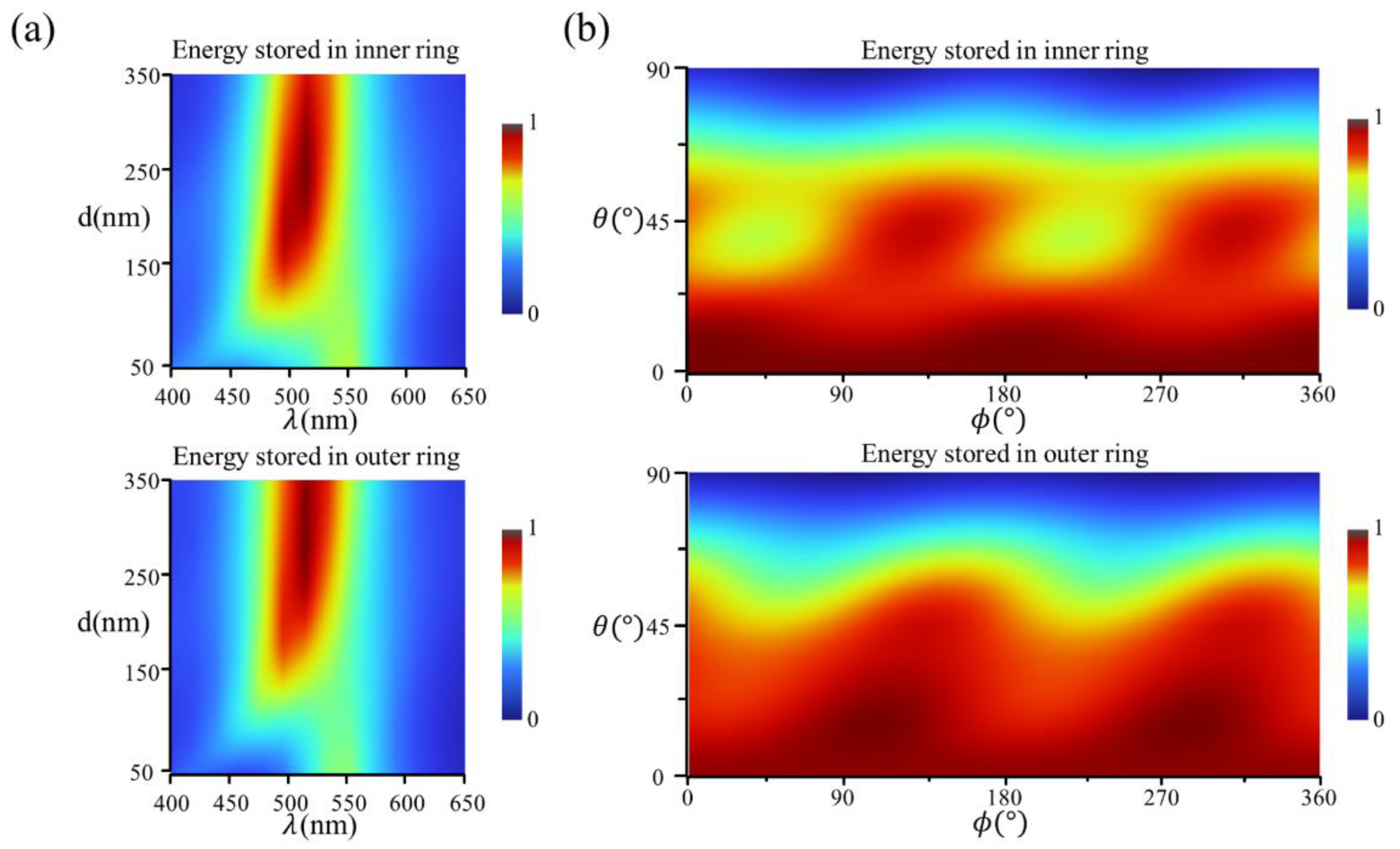
The ratio of the inner and outer energy r = e i / e o is a function of ( θ , ϕ ), from which the 3D light-direction angular sensitivity physical quantity is obtained. For complete concentric nanorings, the response characteristics are polarization-independent due to the strict pairwise nature of the structure, and the energy stored in the inner and outer ring differs from the spacing d and the wavelength of incident light λ , as shown in Figure 2a with the normal incident at s-polarization. In this paper, d is set as 100 nm and λ is set as 550 nm within the absorptive band of Si material to ensure moderate stored energies in both inner and outer rings for ratio comparison analysis and actual detection as shown in Figure 2a. Meanwhile, the ( θ , ϕ ) influences the resonances within the inner and outer nanorings further determine the energy stored as shown in the top and bottom of Figure 2b, respectively.
2.2. 3D Light-Direction Sensor
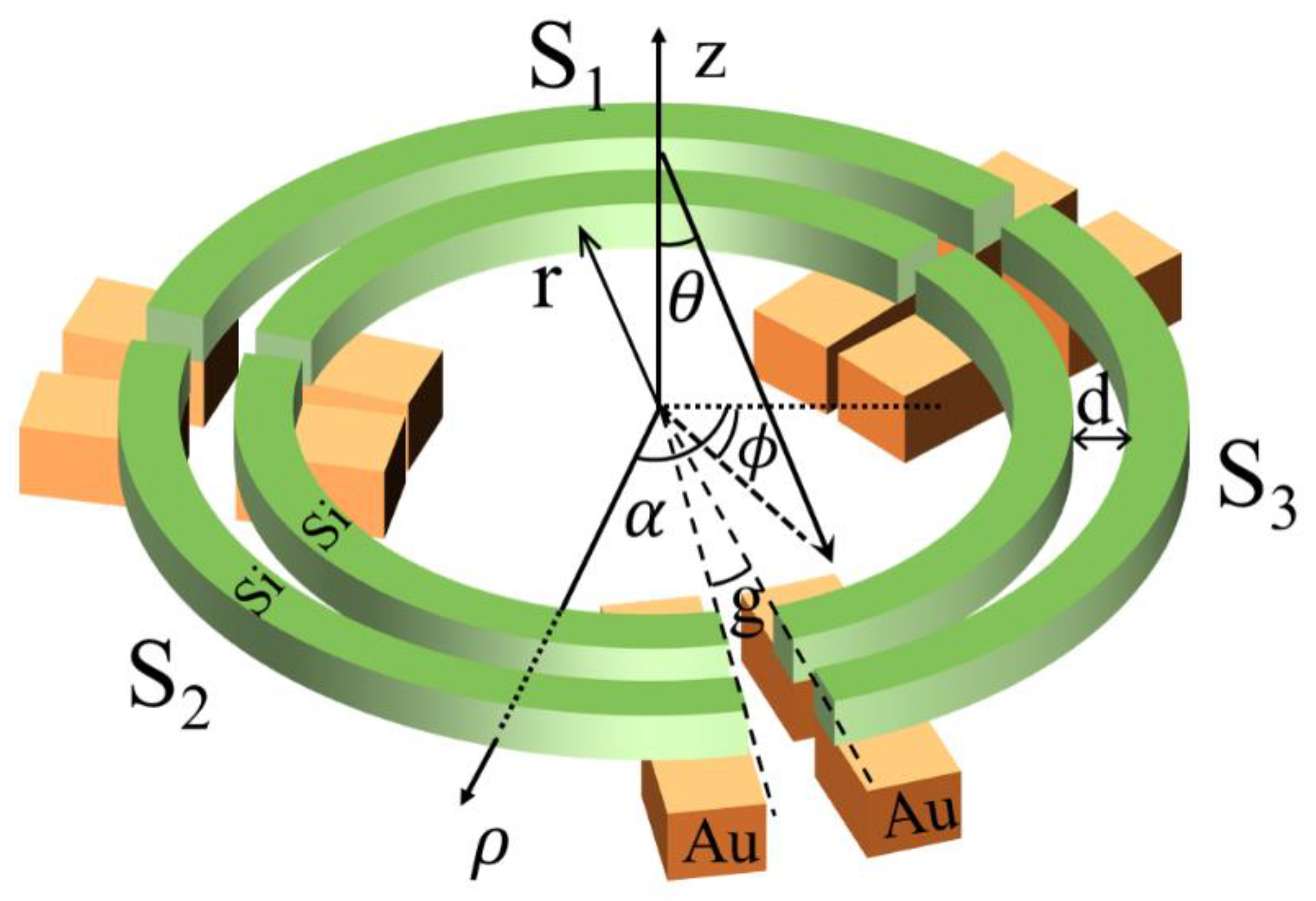
To achieve 3D light-direction sensing with a single pair, the response of its structure must exhibit continuous, sensitive, uniform, and monotonous dependence on both the elevation ( θ ) and the azimuth ( ϕ ) simultaneously within the detection range. Due to the circular symmetry, the energy stored in the complete nanoring is independent of ϕ . Thus, it is necessary to segment the nanorings to introduce azimuth angle sensitivity, and for full ϕ sensing, at least three segments are needed as proposed in Figure 3. Assuming that the nanorings are segmented into three pairs: S1  ( α ( 0,120 o ) ) , S2  ( α ( 120 o , 240 o ) ) , and S3  ( α ( 240 o , 360 o ) ) , the energy stored in the inner and outer segments within the same pair can be calculated as:
e i j / o j = S j | a i j / o j ( α ) 2 d α ,   j = 1 , 2 , 3
where the energy stored in pairs S1, S2, S3 is S j = e i j + e o j . According to the equations derived above, physical quantities on energy distribution exhibiting strong angles correlations can be induced, which including the ratio of energy between the inner and the outer segment within the same pair ( e i j / e o j ), and the ratio of energy stored by different pairs ( S j / S j + 1 m o d   3 ) . Both quantity-ratios demonstrate a strong functional dependence on the angles ( θ , ϕ ), enabling accurate 3D light-direction angles calculation, which will be elaborated in detail in the discussion section.
In working, the energy in the resonator’s segments can be further quantified as photocurrent responses. Thus, the incident angle can then be calculated by the photocurrents exported from metal (Au/Al) electrodes of the nanoring segments [27]. Additionally, considering the practical working condition and stability of devices, the structure is fabricated on a silicon dioxide (SiO2) substrate and most of the architecture, excluding the metal electrodes, is protected by SiO2 to afford resistance to temperature and humidity.
In summary, the principle of high sensitivity for the segmented concentric nanorings is similar to the angular dependence expounded in the parallel straight nanowires [13]. The non-Hermitian coupling between the inner and outer segments of the same nanoring-pair results in strong angular dependence on elevation. Therefore, θ can be calculated by the ratio of photocurrents between these two segments (RPS). While, the differences in responsivities among the nanoring-pairs enable azimuthal determination, as the resonance in each pair especially depends on the azimuth. Consequently, ϕ can be calculated by the ratio of total photocurrents between adjacent nanoring-pairs (RPP). Through reasonable adjustments, including the number of segments and structural parameters, higher precision of the 3D light-direction angles detection can be obtained. Moreover, the proposed structure behaves high symmetry to ensure translational responses to the polarization of the incident light, indicating computational universality.
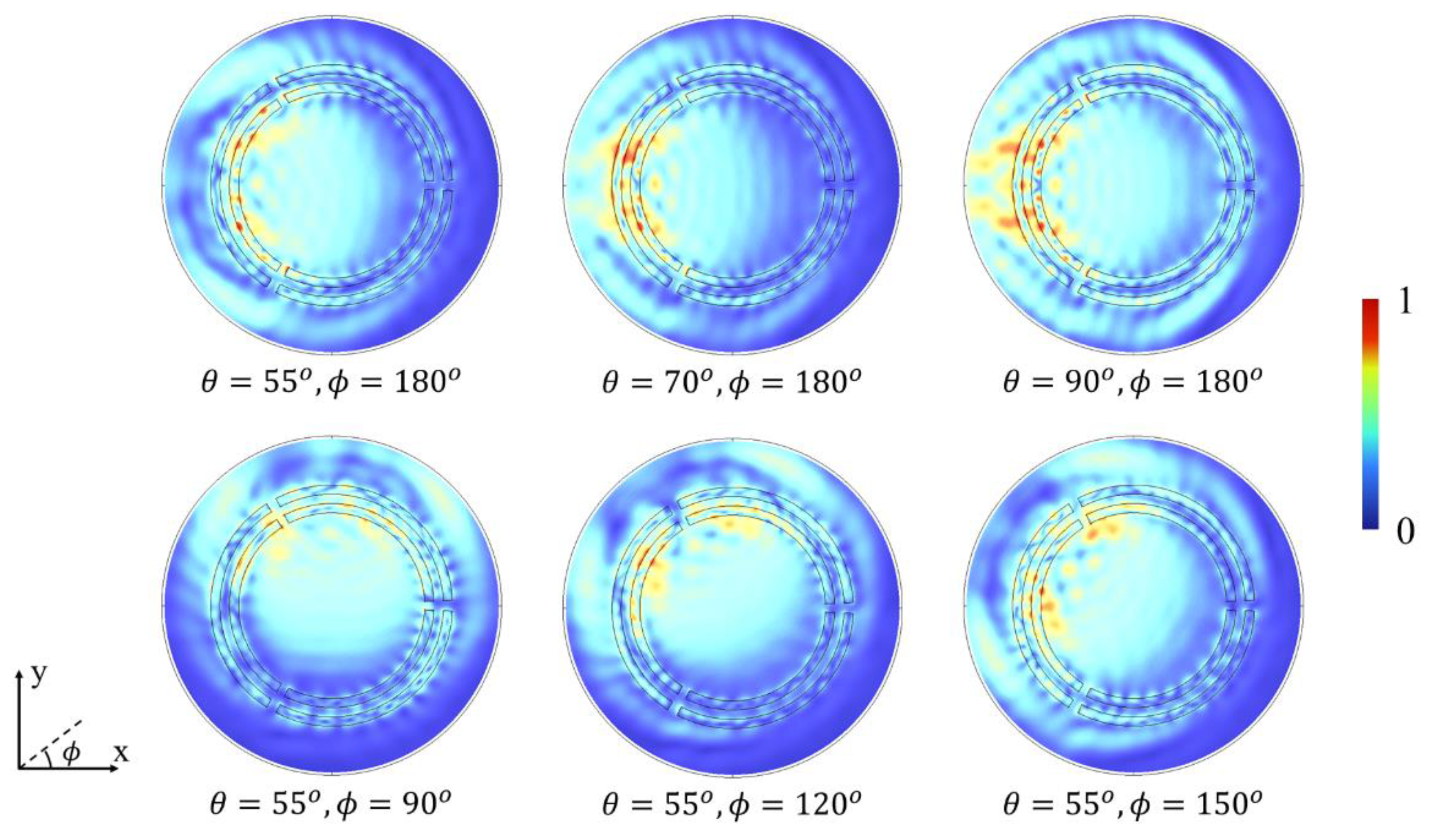
For the numerical simulations of light energy absorption of different ( θ , ϕ ) in the proposed segmented concentric nanorings, 3D finite element method (FEM) by commercial software COMSOL was employed in wavelength domain. As shown in Figure 4, the normalized electric field distribution varies with θ and ϕ , demonstrating obvious angular sensibility due to the resonance in the structure, confirming its functionality for 3D light-direction sensing.

2.3. Deep Learning for Data Fitting

Deep learning (DL) offers exceptional capabilities for multidimensional data fitting and inference. According to the universal approximation theorem [28,29,30,31], neural networks used for deep learning can approximate any function under certain conditions. For the proposed angle sensor, modeling the physical relationship between the ( θ , ϕ ) and several response variables to calculate the angles from these corresponding data is challenging using traditional methods. In detail, the interdependence between θ and ϕ will lead to an expansion of response data dimensions beyond the computing and fitting ability of traditional analysis methods. While, DL can address this challenge due to its ability to fit high-dimensional data, and even potentially can enhance both accuracy and detection range.
In this work, a fully connected neural network (FCNN) with three hidden-layers and a width of 512 neurons per layer is employed as shown in Figure 7, utilizing the rectified linear unit (ReLU) as the activation function. After sufficient training of 5000 epochs, the DL model can accurately fit and infer θ and ϕ from the response data generated by the sensor structure. The fitting accuracy during the training is measured by the mean squared error (MSE), while the model’s performance is quantified by the absolute error (ABS) between the calculated 3D light-direction angles and the targets using a pre-divided test dataset.

2.4. Fabrication Process

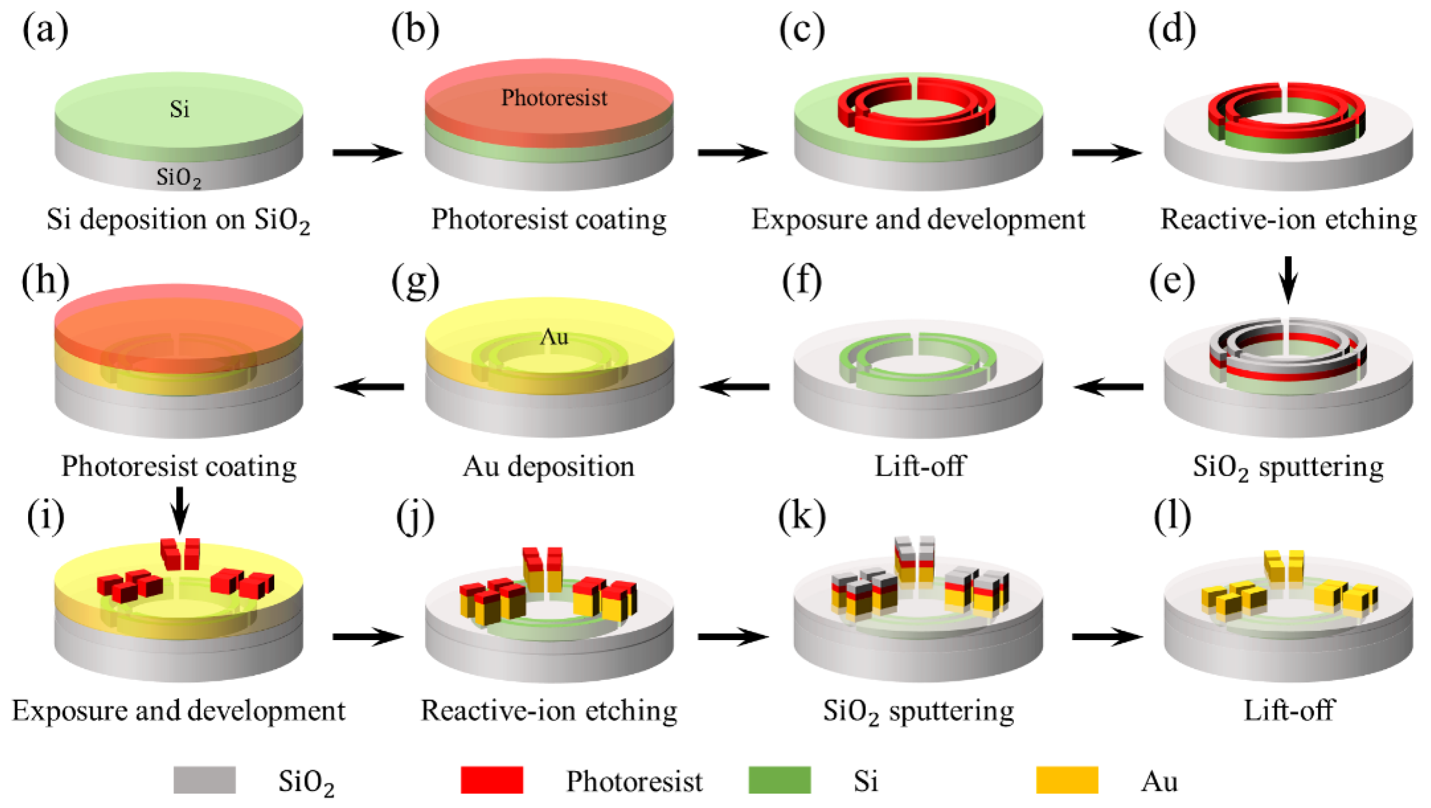
The fabrication of the segmented concentric nanorings include the electron-beam lithography (EBL), deposition, and lift-off, as shown in Figure 5. Specifically, firstly, a 100nm-thick lightly n-doped poly-Si layer is deposited on the SiO2 substrate using low-pressure chemical vapor deposition (LPCVD). Then, after the photoresist coating, EBL is employed to define the mask patterns followed by dry etching to create the segmented Si nanorings. Subsequently, a 100nm-thick SiO2 layer is deposited to cover the nanorings. After lifting off the photoresist, similar processing steps are used to fabricate Au contacts. EBL is used to define the contact patterns, followed by electron-beam physical vapor deposition of Au. The resulting electrodes extend beyond the sensor, facilitating circuit wiring and integration.

3. Results

In the simulation, the three-segment nanorings shown in Figure 3 represents the minimum segment configuration required to achieve full azimuthal detection. The width ( w ) and height ( h ) of the nanorings are both 100 nm, and the spacing ( d ) between the inner and outer nanorings within the same pair is 100 nm. The inner radius of the nanoring ( r ) is 1000 nm, and the central angle ( g ) corresponding to the gap between adjacent nanoring-pairs is 5 o .
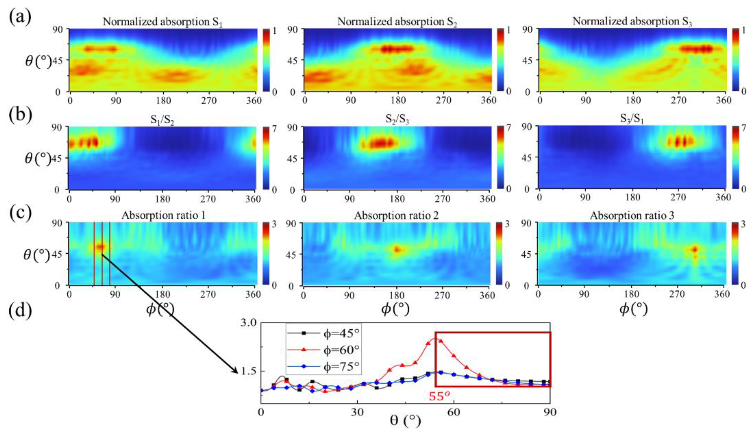
To elucidate the angular dependence of absorption, detailed absorption maps of the sensor under different incident elevations ( θ ) and azimuths ( ϕ ) at the wavelength ( λ ) of 550nm are presented in Figure 6. The results clearly show that the normalized total absorption of the inner and outer nanoring segments within the same pair (Figure 6a), the ratio of total absorption between adjacent nanoring-pairs (Figure 6b), and the ratio of absorption between the inner and outer nanoring-segments within each pair (Figure 6c) all exhibit clear sensitivity to both θ and ϕ within a specific range of θ (Figure 6d).
From Figure 6d, it can be observed that the detection range for θ , i.e., the monotonic range for specific ϕ that can be fitted by DL, is approximately 35 o ( 55 o 90 o ), which is the target range for subsequent calculation. The detection range for θ can be converted and adjusted through a waveguide, where the light in the waveguide obeys the total internal reflection larger than the critical angle. Additionally, due to the translational relationship of responsivities with respect to ϕ between different pairs, the detection range for ϕ is expected to be full of 360 o .
Meanwhile, due to the symmetry and translation properties of the proposed structure and its responses as shown, analyzing 1/3 of the sensor is sufficient to verify the overall functionality. Taking ϕ within ( 60 o , 180 o ) as an example, whose calculation method is the same as the other ranges, and θ within the computable range of ( 55 o , 90 o ) as illustrated earlier. The FCNN is employed to achieve DL, with the training data inputs consisting of S1/S2, S2/S3, S3/S1, ratio 1, ratio 2, ratio 3, and targets including θ and ϕ .
Based on the test results, the average ABS for θ is 0.372 o with a maximum of 2.077 o , and for ϕ , the average ABS is 0.35 o with a maximum of 2.55 o . The sensor demonstrates consistent detection capabilities for both θ and ϕ within its detection range, and its performance in ( θ , ϕ ) calculation is sufficient for most application scenarios.

4. Discussion

4.1. 3D Light-Direction Angles Calculation

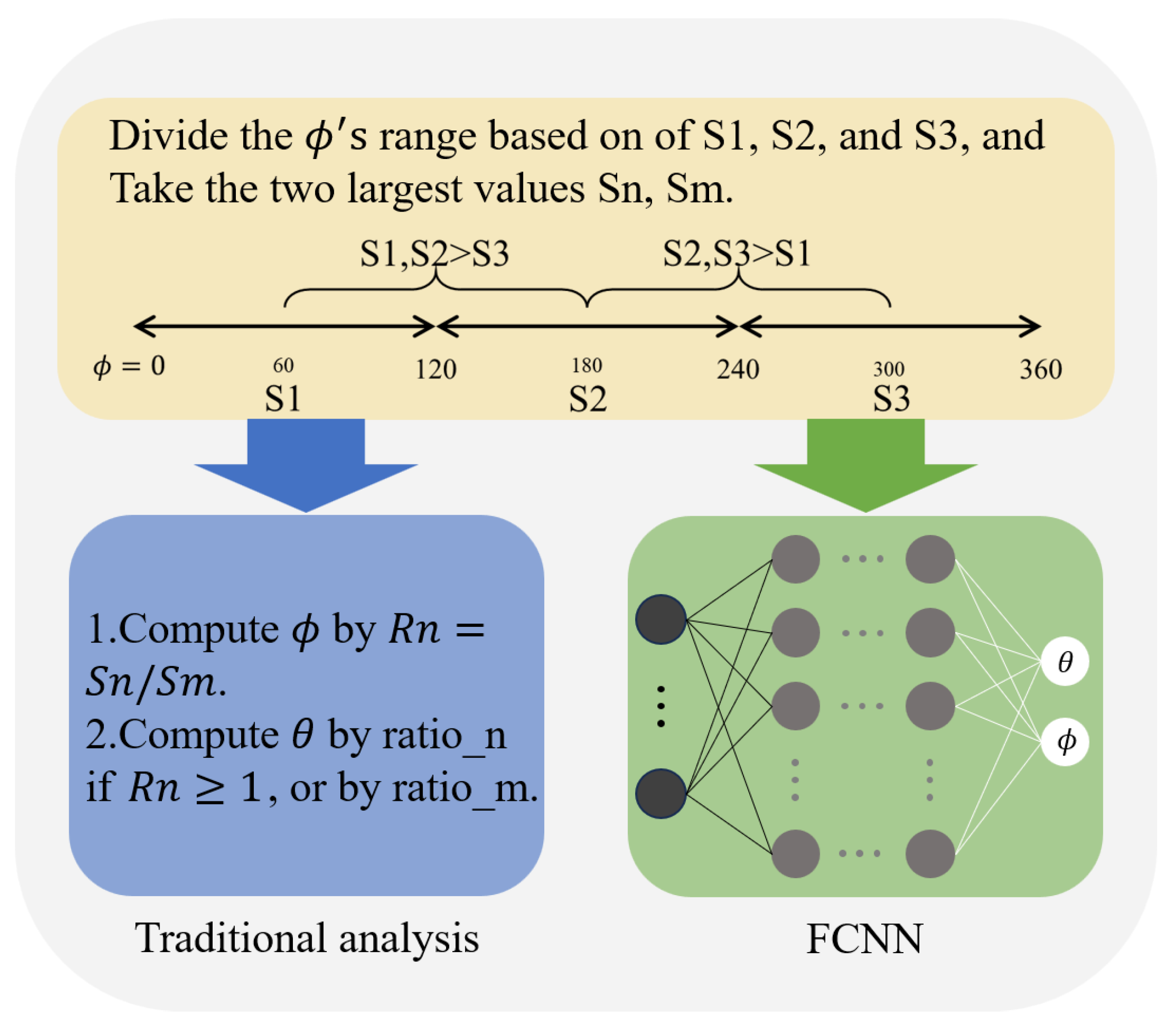
Based on the angles detection principle of the proposed segmented nanorings, θ can be calculated by the ratio of photocurrents between the two segments (RPS), and ϕ can be calculated by the ratio of total photocurrents between adjacent nanoring-pairs (RPP). As shown in Figure 7, the precise ( θ , ϕ ) can be determined based on the corresponding responses, which exhibit high sensitivities to θ and ϕ .
To compute the angles from the responses of the structure, we follow these two steps below: Firstly, preliminarily divide the range of incident azimuth ( ϕ ) into 120 o steps based on the response amplitudes of the segmented nanoring-pairs. This is because the coupling in the pair centered towards the incident light will be the strongest, as shown in Figure 6a. Traditionally, θ might be calculated by RPS and ϕ by RPP independently. However, due to the interdependence between θ and ϕ , this approach is not feasible. To address this issue, we use a fully connected neural network (FCNN) for deep learning (DL), which treats θ and ϕ as a combined problem, fitting and inferring them from all responses with high-precision and a wide-sensing-range. This method overcomes the limitations of traditional techniques and leverages the powerful data-fitting capabilities of DL to achieve accurate θ , ϕ measurements.

4.2. More Segments to Improve Detection

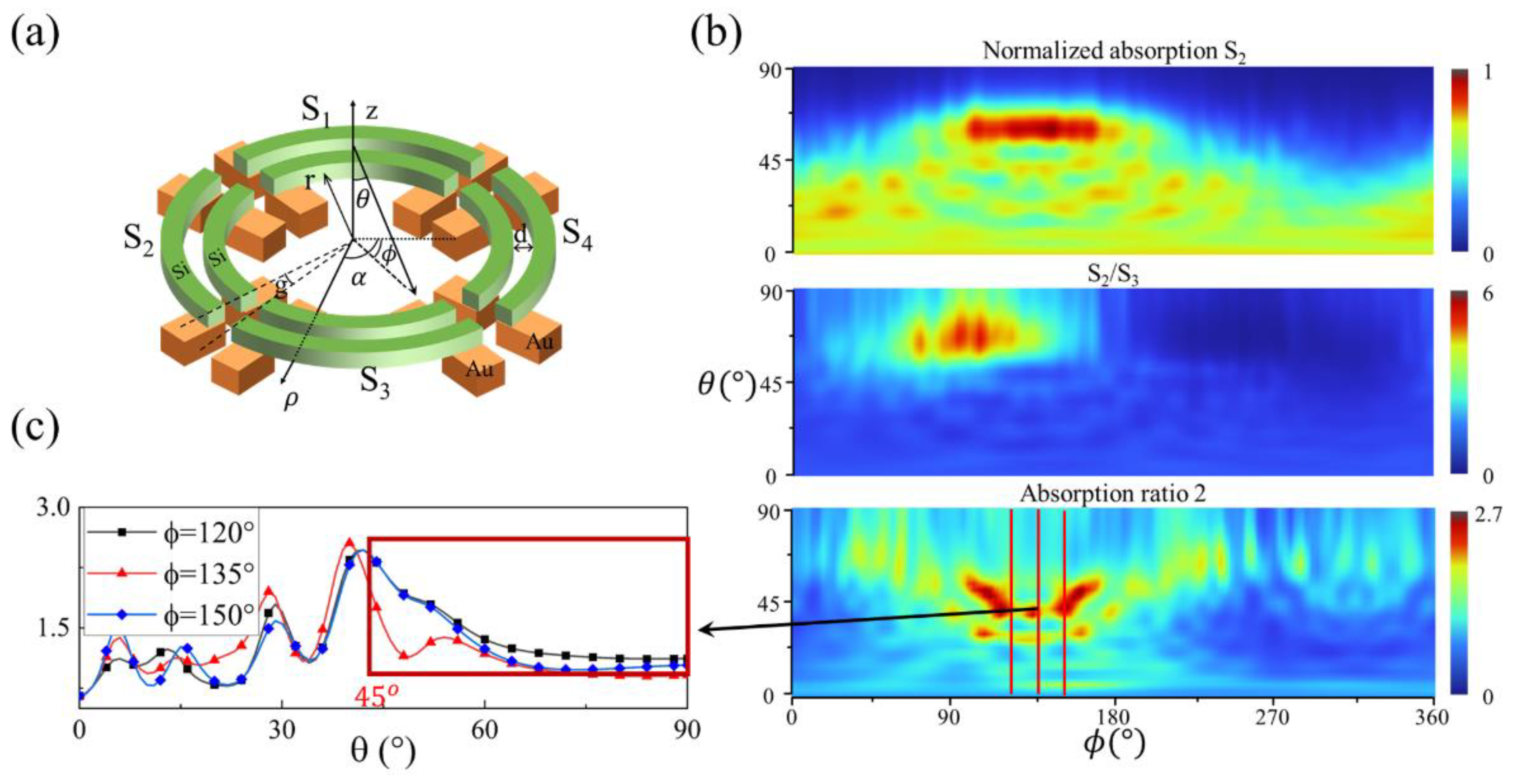
The number of segments in the proposed sensor significantly impacts the accuracy of the angles’ calculation due to its effect on coupling among the nanoring-segments. Increasing the number of segments may enhance both the range and accuracy of the ( θ , ϕ ) detection. Following the same method, the four-segment concentric nanorings with the same structural parameters as the 3-segment structure are simulated and tested (Figure 8a), with partial results presented in Figure 8b as examples. Shown as in Figure 8c, the absorption ratio result shows that the detection range for θ has been expanded to approximately 45 o ( 45 o 90 o ), where the absorption ratio descends monotonically with θ for specific ϕ values.
As with the 3-segment structure, a DL network is used to fit the response data and determine the 3D light-direction angles for the 4-segments configuration. As shown in the results, the average ABS for θ is 0.187 o with a maximum of 2.252 o , and for ϕ , the average ABS is 0.174 o with a maximum of 1.704 o , indicating that the angular detection capability has been further improved to be better than that of the 3-segments because of more segments. However, it is important to note that although increasing the number of segments may improve detection range and accuracy, it also raises manufacturing difficulty and costs, thus trade-off needs to be considered.

4.3. Cross-Arranged Nanowire-Pairs for 3D Light-Direction Sensing

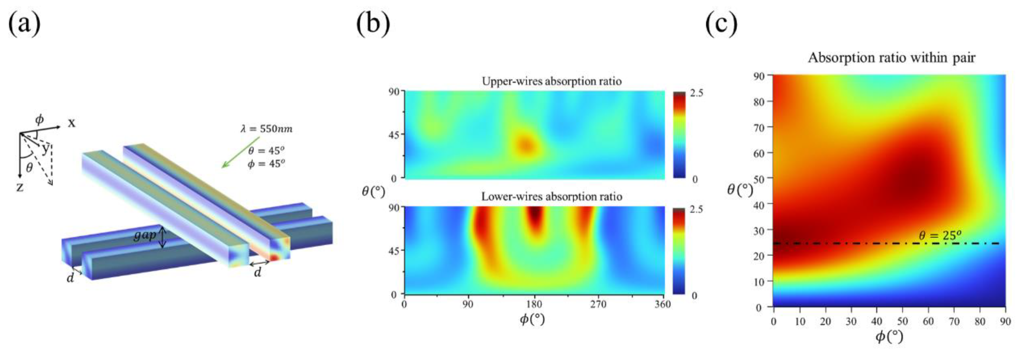
By the way, the combination of the resonant-nanowires can be intuitively expected to expand the detection dimension and function as a angle sensor (Figure 9a). In the simulation, nanowires with a width and height of 100 nm and a length of 500 nm, wrapped in SiO2, are divided into two pairs that are internally coupled and arranged in a vertical cross-configuration with a specified distance (gap) between them.
With the gap of 100 nm, shown in Figure 9b, the response of the composite structure for different θ and ϕ does not exhibit a consistent regularity over a wide range, making it impossible to accurately reconstruct large-range 3D light-direction angles. The response of the upper layer differs from that of the lower layer, which is likely due to the interference of the upper-layer nanowires on the incident light, causing the light received by the lower-layer nanowires to differ from the original incident light.
To eliminate the interference between the upper layer and the lower layer, when the gap is large enough ( g a p λ ), taking a gap of 1 μ m as an example, the response of the two pairs becomes symmetrical. The absorption ratio between the two nanowires within a pair is shown in Figure 9c, exhibiting regular characteristics within a certain range of θ ( 0,25 o ) . In this range, the RPN changes monotonically with respect to θ for a specific ϕ , enabling the calculation of the ( θ , ϕ ) via DL.
Using the same DL fitting method as before, for θ ( 0,25 o ) , and taking ϕ ( 0,45 o ) as an example, which represents the entire structure because of its symmetry, the average ABS for θ is 0.198 o with a maximum of 0.578 o and the one for ϕ is 0.948 o with a maximum of 16.387 o in the test. It is clear that although the cross-arranged nanowire-pairs can detect ( θ , ϕ ) when the distance between the upper layer and the lower layer is sufficiently large, but the calculation error for ϕ is significantly higher than for θ , which indicates that the sensitivity of the device response to these two angles is inconsistent, rendering it impractical for applications requiring uniform sensitivity.
By contrast, the proposed segmented nanorings, with their segmented and circular characteristics, can sense 3D light-direction angle with a smaller thickness, a wider detection range, and uniform angular sensitivity (Table 1), which demonstrates that the segmented nanorings structure offers better and more stable angle detection capabilities and a wider detection range than the cross-arranged nanowire-pairs. The configuration of segmented concentric nanorings ensures consistent detection capabilities for both θ and ϕ , making it more suitable for practical applications, and it can be inferred that more segments will lead to further improvement.
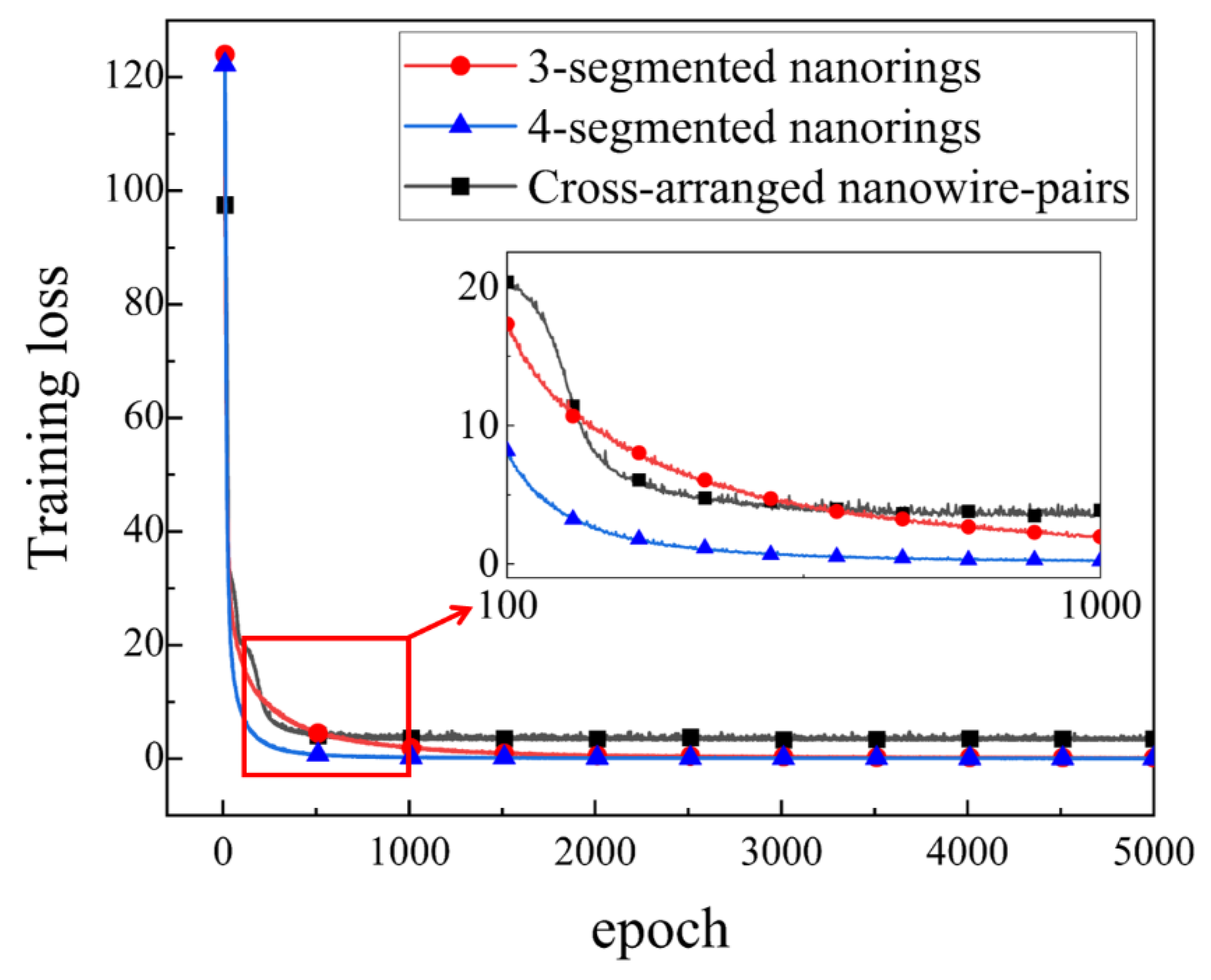
Additionally, during the DL training process, dividing more segments can result in faster convergence speeds and smaller losses (Figure 10). These improvements may stem from the expansion of response data dimensions brought about by additional segments and the stronger resonance caused by smaller nanoring-lengths, which provide computational benefits such as cross-validation between these data in the DL model.

5. Conclusion

To achieve precise 3D light-direction angle detection with a single sensing unit, we propose a structure of segmented concentric nanoring-pairs absorptive resonators. This structure exhibits strong and uniform angular sensitivity to both elevation and azimuth angles. By employing deep learning for data fitting, the sensor can achieve a detection range of 0 360 o for azimuth and 45 o 90 o for elevation with an average accuracy of 0.19 o in the ( θ , ϕ ) angle sensing, thereby meeting the requirements of most application scenarios. The accuracy and range of angles sensing can be improved with the increase of the number of segments. Finally, based on the structure of segmented concentric nanorings, by combining its resonance characters with deep learning, angle sensing precisely is enable, showing various promising applications such as optical field reconstruction, dynamic ranging, optical interaction, and even military reconnaissance and guidance can be achieved by their array integration.

Author Contributions

Conceptualization, P.H., P.W. and Z.G.; methodology, P.H., P.W. and Z.Y.; software, P.H. and P.W.; validation, P.H.; investigation, P.H.; data curation, P.H. and Z.G.; Funding acquisition, Z.Y.; writing—original draft preparation, P.H. and P.W.; writing—review and editing, P.H. and Z.Y. All authors have read and agreed to the published version of the manuscript.

Funding

This research was funded by the Natural Science Foundation of the Fujian Province, China, grant number 2023J01234.

Data Availability Statement

The raw data supporting the conclusions of this article will be made available by the authors on request.

Conflicts of Interest

The authors declare no conflicts of interest.

References

  1. Adelson, E.H.; Bergen, J.R. The plenoptic function and the elements of early vision; Vision and Modeling Group, Media Laboratory, Massachusetts Institute of …: 1991; Volume 2.
  2. Ng, R.; Levoy, M.; Brédif, M.; Duval, G.; Horowitz, M.; Hanrahan, P. Light field photography with a hand-held plenoptic camera. Stanford university, 2005.
  3. Wang, A.; Gill, P.; Molnar, A. Light field image sensors based on the Talbot effect. Applied optics 2009, 48, 5897–5905. [Google Scholar] [CrossRef]
  4. Wang, A.; Molnar, A. A light-field image sensor in 180 nm CMOS. IEEE Journal of Solid-State Circuits 2011, 47, 257–271. [Google Scholar] [CrossRef]
  5. Li, Q.; van de Groep, J.; Wang, Y.; Kik, P.G.; Brongersma, M.L. Transparent multispectral photodetectors mimicking the human visual system. Nature Communications 2019, 10, 4982. [Google Scholar] [CrossRef] [PubMed]
  6. Yu, L.; Feng, X.; Hu, P.; Lin, X.; Jing, T. Development of a 3-DOF Angle Sensor Based on a Single Laser Interference Probe. Micromachines 2023, 14, 2221. [Google Scholar] [CrossRef] [PubMed]
  7. Koch, C.; Oehm, J.; Emde, J.; Budde, W. Light source position measurement technique applicable in SOI technology. IEEE journal of solid-state circuits 2008, 43, 1588–1593. [Google Scholar] [CrossRef]
  8. Yi, S.; Xiang, J.; Zhou, M.; Wu, Z.; Yang, L.; Yu, Z. Angle-based wavefront sensing enabled by the near fields of flat optics. Nature communications 2021, 12, 6002. [Google Scholar] [CrossRef]
  9. Li, D.; Liu, S. Research on four-quadrant detector and its precise detection. Int. J. Digital Content Technol. Appl. 2011, 5, 138–143. [Google Scholar]
  10. Azaña, J.; Guillet de Chatellus, H. Angular talbot effect. Physical Review Letters 2014, 112, 213902. [Google Scholar] [CrossRef]
  11. Yi, L.; Hou, B.; Zhao, H.; Liu, X. X-ray-to-visible light-field detection through pixelated colour conversion. Nature 2023, 618, 281–286. [Google Scholar] [CrossRef]
  12. Nanophotonics, R.T. Resonant thermoelectric nanophotonics. 2017.
  13. Yi, S.; Zhou, M.; Yu, Z.; Fan, P.; Behdad, N.; Lin, D.; Wang, K.X.; Fan, S.; Brongersma, M. Subwavelength angle-sensing photodetectors inspired by directional hearing in small animals. Nature nanotechnology 2018, 13, 1143–1147. [Google Scholar] [CrossRef]
  14. Nagarajan, A.; Hara, S.; Satoh, H.; Panchanathan, A.P.; Inokawa, H. Angle-sensitive detector based on silicon-on-insulator photodiode stacked with surface plasmon antenna. Sensors 2020, 20, 5543. [Google Scholar] [CrossRef]
  15. Born, M. Principles of optics - electromagnetic theory of propagation, interference and diffraction of light (7. ed.); Principles of optics - electromagnetic theory of propagation, interference and diffraction of light (7. ed.): 1999.
  16. Barlow, H.B. The size of ommatidia in apposition eyes. Journal of experimental Biology 1952, 29, 667–674. [Google Scholar] [CrossRef]
  17. Zhu, X.; Liang, B.; Kan, W.; Peng, Y.; Cheng, J. Deep-subwavelength-scale directional sensing based on highly localized dipolar mie resonances. Physical Review Applied 2016, 5, 054015. [Google Scholar] [CrossRef]
  18. Lee, T.; Nomura, T.; Su, X.; Iizuka, H. Fano-Like Acoustic Resonance for Subwavelength Directional Sensing: 0–360 Degree Measurement. Advanced Science 2020, 7, 1903101. [Google Scholar] [CrossRef] [PubMed]
  19. Meng, Y.; Hu, X.; Yang, C.; Shen, X.; Cao, X.; Lin, L.; Yan, F.; Yue, T. Angle-sensitive Pixels Based on Subwavelength Compound Gratings. Current Optics and Photonics 2022, 6, 359–366. [Google Scholar]
  20. Bakirova, L.I.; Voronkov, G.S.; Lyubopytov, V.S.; Butt, M.A.; Khonina, S.N.; Stepanov, I.V.; Grakhova, E.P.; Kutluyarov, R.V. Micro-Ring Resonator-Based Tunable Vortex Beam Emitter. Micromachines 2023, 15, 34. [Google Scholar] [CrossRef]
  21. Suh, W.; Wang, Z.; Fan, S. Temporal coupled-mode theory and the presence of non-orthogonal modes in lossless multimode cavities. IEEE Journal of Quantum Electronics 2004, 40, 1511–1518. [Google Scholar]
  22. Torres, J.; Baptista, A.; Machado, V.M. Coupling analysis in concentric ring waveguides. Journal of lightwave technology 2013, 31, 2140–2145. [Google Scholar] [CrossRef]
  23. Verslegers, L.; Yu, Z.; Ruan, Z.; Catrysse, P.B.; Fan, S. From Electromagnetically Induced Transparency to Superscattering with a Single Structure: A Coupled-Mode Theory for Doubly Resonant Structures. Physical review letters 2012, 108, 083902. [Google Scholar] [CrossRef]
  24. Verslegers, L.; Yu, Z.; Catrysse, P.B.; Fan, S. Temporal coupled-mode theory for resonant apertures. JOSA B 2010, 27, 1947–1956. [Google Scholar] [CrossRef]
  25. Zhang, S.; Ye, Z.; Wang, Y.; Park, Y.; Bartal, G.; Mrejen, M.; Yin, X.; Zhang, X. Anti-Hermitian Plasmon Coupling of an Array of Gold Thin-Film Antennas for Controlling Light at the Nanoscale. Physical review letters 2012, 109, 193902. [Google Scholar] [CrossRef] [PubMed]
  26. Zhou, M.; Shi, L.; Zi, J.; Yu, Z. Extraordinarily large optical cross section for localized single nanoresonator. Physical review letters 2015, 115, 023903. [Google Scholar] [CrossRef] [PubMed]
  27. Cao, L.; White, J.S.; Park, J.-S.; Schuller, J.A.; Clemens, B.M.; Brongersma, M.L. Engineering light absorption in semiconductor nanowire devices. Nature materials 2009, 8, 643–647. [Google Scholar] [CrossRef] [PubMed]
  28. Cybenko, G. Approximation by superpositions of a sigmoidal function. Mathematics of control, signals and systems 1989, 2, 303–314. [Google Scholar] [CrossRef]
  29. Hornik, K.; Stinchcombe, M.; White, H. Multilayer feedforward networks are universal approximators. Neural networks 1989, 2, 359–366. [Google Scholar] [CrossRef]
  30. Leshno, M.; Lin, V.Y.; Pinkus, A.; Schocken, S. Multilayer feedforward networks with a nonpolynomial activation function can approximate any function. Neural networks 1993, 6, 861–867. [Google Scholar] [CrossRef]
  31. Chen, T.; Chen, H. Universal approximation to nonlinear operators by neural networks with arbitrary activation functions and its application to dynamical systems. IEEE transactions on neural networks 1995, 6, 911–917. [Google Scholar] [CrossRef]
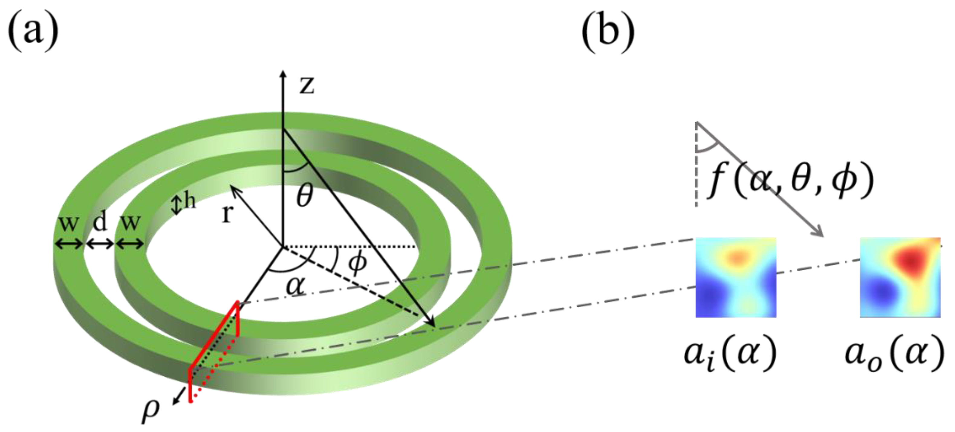
Figure 1. (a) Structural diagram of double concentric Si-nanorings resonators. (b) For the cross-sections determined by the coordinate angle α in cylindrical coordinates ( ρ , α , z ), the effective angle of incident light received is a function of ( θ , ϕ , α ).
Preprints 116963 g001
Figure 2. (a) The maps of normalized absorption intensity of the inner and the outer nanoring with spacing ( d ) and wavelength ( λ ) under normal incident light. (b) numerical maps of normalized absorption intensity of the inner and the outer nanoring for different ( θ , ϕ ) .
Preprints 116963 g002
Figure 3. The structural diagram of the 3-segment double concentric nanorings sensor. Two nanorings are divided into inner and outer rings and further segmented into three pairs: S1, S2, and S3. The inner radius of the nanoring ( r ) is 1000 nm, the width ( w ), height ( h ) of nanorings, and the spacing ( d ) are 100 nm, and the gap between adjacent nanoring-pairs corresponds to a central angle ( g ) is 5 o .
Preprints 116963 g003
Figure 4. The normalized electric field distribution map for different 3D light-direction angles.
Preprints 116963 g004
Figure 5. Schematic of the fabrication procedure for the segmented concentric nanorings. (a) 100 nm-thick Si on SiO2 substrate. (b) Photoresist coating. (c) Electron-beam exposure and development. (d) Reactive-ion etching. (e) SiO2 sputtering. (f) Lift-off. (g) Au deposition. (h) Photoresist coating. (i) Electron-beam exposure and development. (j) Reactive-ion etching. (k) SiO2 sputtering. (l) Lift-off.
Preprints 116963 g005
Figure 6. The response of the 3-segment concentric nanorings sensor to the incident light direction angles, θ and ϕ . (a) The normalized numerical maps of the total absorption of the S1, S2, and S3 nanoring-pairs, including both the inner and outer nanoring-segments within each pair. (b) The numerical maps of the ratio of the total absorption between adjacent nanoring-pairs, S1/S2, S2/S3, and S3/S1. (c) The numerical maps of the ratio of the absorption between the inner and outer nanoring segments within each pair, ratio 1, ratio 2, and ratio 3 (e.g., ratio 1 is for the S1 pair). (d) For specific ϕ , 45 o , 60 o and 75 o , the absorption ratio for each pair decreases monotonically concerning θ within the range of ( 55 o , 90 o ), which is the computable range for θ .
Preprints 116963 g006
Figure 7. The approach for 3D light-direction angles analysis and calculation. First, an initial division of the azimuth can be made according to the numerical values of the segmented nanorings responses, which helps to select the data sources for accurate ( θ , ϕ ) calculation. Then, traditional analysis methods or neural networks may be used to compute the elevation and azimuth accurately. The former is not feasible because traditional methods are unable to deal with multidimensional data, and we consider using the fully connected neural network (FCNN) to fit the relationship between the responses and the ( θ , ϕ ) , especially the interdependence between the elevation and azimuth.
Preprints 116963 g007
Figure 8. The structural diagram and response of the 4-segmented nanorings sensor. (a) The structure of the 4-segments. The nanorings are segmented into four pairs: S1, S2, S3, and S4 with the same structural parameters as the 3-segment structure. In detail, the inner radius of the nanoring (r) is 1000 nm, the width ( w ) and height ( h ) of nanorings and the spacing (d) are 100 nm, and the gap between adjacent nanoring-pairs corresponds to a central angle ( g ) is 5 o . (b) The response of the 4-segment structure. As the 3-segments, the responses of the 4-segment also appear translational symmetry. We present the normalized numerical map of the total absorption of the S2 pair, the numerical map of the ratio of S2 and S3, and the corresponding absorption ratio of inner and outer rings within S2 (ratio 2) as examples. (c) From the characteristics of ratio 2, it can be seen that the monotonical range of θ has expanded to approximately ( 45 o , 90 o ), which is the computable range for θ .
Preprints 116963 g008
Figure 9. The structure and response of the cross-arranged nanowires sensor to the ( θ , ϕ ) . (a) Two pairs of vertically cross-arranged coupled nanowires, with a vertical distance (gap) of 100 nm. The nanowires have a width and height of 100 nm, a length of 500 nm, and an internal spacing (d) of 100 nm within each nanowire pair. (b) The numerical maps of the absorption ratio within the upper and lower nanowire pairs with g a p of 100 nm concerning θ and ϕ . The response of the upper layer is different from that of the lower layer, and they don’t exhibit a consistent regularity over a wide range of angles to compute the angles. (c) The numerical map of the absorption ratio between the two nanowires within a pair when the gap is 1 μ m . When the gap is large enough ( g a p λ ), the two pairs can be analyzed separately, and their responses have angular symmetry. According to the map, the absorption ratio within pair is monotonically changing concerning θ for a specific ϕ when θ ( 0,25 o ) and this range is the detection range for θ .
Preprints 116963 g009
Figure 10. The loss descent curve during the training process of deep learning models corresponding to different structures. (To distinguish clearly, the first 10 epochs corresponding to the loss have been taken out.).
Preprints 116963 g010
Table 1. The absolute error of θ and ϕ for different angular detection structures, including the detection range for θ (the detection ranges for ϕ are all 360 o ), average absolute error, maximum absolute error, and the variance of it.
Structure Detection   range   for   θ   ( ° ) Absolute   error   of   θ   ( ° ) Absolute   error   of   ϕ   ( ° )
Average Maximum Variance Average Maximum Variance
3-segmented
nanorings
55-90 0.372 2.077 0.121 0.350 2.550 0.102
4-segmented
nanorings
45-90 0.187 2.252 0.041 0.174 1.704 0.030
Cross-arranged nanowire-pairs 0-25 0.198 0.578 0.009 0.948 16.387 7.291
Disclaimer/Publisher’s Note: The statements, opinions and data contained in all publications are solely those of the individual author(s) and contributor(s) and not of MDPI and/or the editor(s). MDPI and/or the editor(s) disclaim responsibility for any injury to people or property resulting from any ideas, methods, instructions or products referred to in the content.
Copyright: This open access article is published under a Creative Commons CC BY 4.0 license, which permit the free download, distribution, and reuse, provided that the author and preprint are cited in any reuse.
Prerpints.org logo

Preprints.org is a free preprint server supported by MDPI in Basel, Switzerland.

Subscribe

© 2024 MDPI (Basel, Switzerland) unless otherwise stated