Preprint
Article

A New Concept of Reconfigurable Antenna Structure Based on an Array of RF-MEMS Switches

Altmetrics

Downloads

94

Views

43

Comments

0

A peer-reviewed article of this preprint also exists.

Submitted:

02 September 2024

Posted:

03 September 2024

You are already at the latest version

Alerts
Abstract
A Geometrical re-configurable structure based on RF Micro-electro-mechanical switches (RF-MEMS) is proposed in this work. The structure is composed of an array of gold metallic patches interconnected together utilizing RF-MEMS switches in order to change its geometry and, consequently, the scattering parameters. In particular, the reconfigurability is achieved by activating multiple RF-MEMS switches, which enables the change of electrical length and, consequently, the resonance frequency of the structure. As a proof of concept, an experimental antenna prototype composed of an array of 7 × 7 elements interconnected by a set of RF-MEMS switches has been designed, fabricated numerically and experimentally assessed. The structure can be set as an antenna or other basic radio frequency components. The obtained experimental results are in good agreement with the simulations, with an error of less than 5% for the considered radiating structures. The quite promising results demonstrated the potentialities and flexibility of the proposed structure.
Keywords: 
Subject: Engineering  -   Telecommunications

1. Introduction

New generation of telecommunication systems, such as mobile smartphones, offers more than multimedia-based services that require high reconfigurability despite the limited dimensions of the devices. Overcrowding of the radio band has been a constant problem within the tumultuous revolution in wireless technology over the decades [1]. There has been growing interest in developing reconfigurable or smart antennas in recent years due to the increasing demand for flexible, multi-functional devices that can adapt to changing communication requirements and environments. These antennas can modify in real time their radiating characteristics [2,3,4], and they can play a key role in any communication system since can alter their physical or electrical properties in order to optimize their performance for a particular application or operating environment. The most diffused reconfigurable antennas are the fully adaptive arrays. They are radiating systems able to modify their radiating properties by continuously changing amplitudes and phases of the power supply of each array element. Different well-known analytical methodologies exist for the optimal synthesis of the array elements, as in [5,6]. Other methodologies make use of evolutionary algorithms, such as genetic algorithm (GA) [7,8,9] or particle swarm optimizer (PSO) [10,11,12], have been used effectively for control the radiating properties of linear or planar arrays. These techniques effectively simplify the hardware and, simultaneously, limit the costs, operating only on the phase of array elements [13,14]. To further simplify the hardware complexity [15] of adaptive antenna systems, some simplified radiating structures called parasitic antennas have been considered. Parasitic antennas consist of only a single active element (connected to the antenna port) and several parasitic structures surrounding the active element. The parasitic elements can be connected to different passive electronically controlled loads aimed at modifying the radiation properties of the active element [16,17]. Recently, this class of antennas has also been adopted in the framework of adaptive antenna systems [18]. Reconfigurable antennas can improve system performance by providing improved gain, bandwidth, efficiency, and reduced interference and power consumption [19], and they are particularly useful in situations where the operating environment is dynamic or uncertain. A variety of new technologies have been used to realize reconfigurable antennas, including liquid metal [20] electronic switches [21,22] such as pin diode [23], varactors, and mechanically reconfigurable elements [24,25]. One promising approach to reconfigurable antenna design is using Micro-Electro-Mechanical Systems (MEMS) technology [26]. MEMS technology offers a particularly promising approach for developing reconfigurable antennas due to its ability to create microscale electromechanical devices with high reliability and low cost [26]. MEMS devices can be fabricated using established microelectronic processes and can be integrated with other electronic components on a single substrate to create highly integrated and compact systems [27]. This makes MEMS technology particularly well-suited for realizing reconfigurable antennas for use in portable and mobile communication systems. Current results show that the MEMS antenna has a significantly wider tuning range than the fixed-tuned patch antenna, with a maximum gain improvement of over 3 dB in certain frequency bands. The MEMS antenna also exhibits lower sensitivity to changes in the operating environment, such as temperature and humidity, compared to the fixed-tuned patch antenna. These results demonstrate the potential of MEMS technology to enable highly adaptable and reliable communication systems for use in the X-band frequency range. RF-MEMS technology was initially developed to replace GaAs HEMT switches and p-i-n diodes for low-loss switching networks and X-band to mm-wave phase shifters. MEMS-based reconfigurable antennas are attractive due to their small size, low cost, very low loss properties (high device Q), its simple microwave circuit model, low power consumption, its high power (voltage/current) handling capabilities (such as the Menlomicro company devices) and ease of integration with other microelectronic components [26]. These characteristics make them suitable for various applications, including wireless communication [28], radar, and satellite systems [29]. In particular [30], X-band MEMS reconfigurable antennas have garnered significant attention due to their ability to operate in the X-band frequency range (8-12 GHz), which is commonly used for satellite [30] and radar applications [31]. Despite the potential benefits of X-band MEMS reconfigurable antennas, their practical implementation has been limited by several challenges. One of the main challenges is achieving a wide reconfiguration range while maintaining sufficient radiation efficiency and stability [32]. In addition, there are also challenges related to the design and fabrication of the MEMS switching elements [33]. To address these challenges, several recent research efforts have focused on developing novel X-band MEMS reconfigurable antenna designs and fabrication techniques [23]. Others many practical engineering applications make use of RF MEMS and obtained very good performances [35,36]. In [37,38,39] preliminary attempts to fabricate reconfigurable hairpin filters are reported, while in [40,41,42,43,44,45], different reconfigurable microwave devices are reported. MEMS are very useful for wireless sensors [46] and reconfigurable antennas [47]. RF- MEMS show very good performance in switching speed (reduced up to a few μ S ), scattering parameters and power consumption, and they demonstrated to work properly up to 100 GHz. This work presents a new kind of reconfigurable antenna based on MEMS switches. The proposed structure acts similarly to a field-programmable gate array (FPGA), a configurable integrated circuit. It consists of square gold blocks that can be connected together thanks to a set of electronic MEMS switches. By properly activating the MEMS switches, the gold blocks can be configured and interconnected together to obtain different geometrical structures able to implement frequency reconfigurable antennas, impedance transformers and other basic RF components. As a proof of concept, an experimental prototype consisting of 7 × 7 gold patches interconnected by means of a set of RF-MEMS switches is designed, fabricated, numerically and experimentally assessed. The proposed solution is monolithic, since all the structures are made in a single technology and a single chip, like MEMs switches, this is the main key of force which makes the proposed prototype compact, simple and with very low power consumption. The paper is structured as follows: section two details the reconfigurable matrix structure based on RF-MEMS. A detailed description of the development and fabrication of a prototype is reported in section three. Section four is devoted to the numerical and experimental assessment of a prototype. Finally, section five reports the conclusions and ideas for further work.

2. Reconfigurable Antenna Structure

In this section, the reconfigurable matrix structure is detailed. It consists of gold square patches sets that can be interconnected using radio frequency MEMs. Each gold patch has four and three MEMs switches for the central and boundary patches, respectively. The total length of the structure L is given by the following:
L = N p × D + N p 1 G
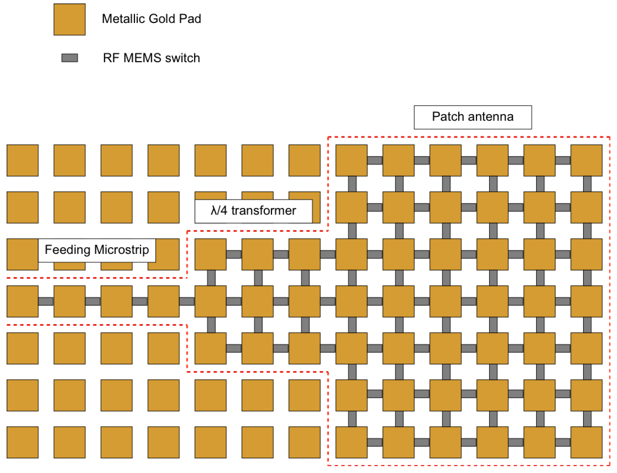
where N p and D are the number and size of gold square patches, respectively. G is the MEMs length. As it can be noticed from Figure 1 the structure is modular, different matrices can be combined together in order to create complex geometries. In particular, conductive traces can be obtained by properly activating the MEMs switches. Figure 2 reports an example of a patch antenna equipped with a quarter wavelength transformer and a feeding microstrip, as it can be noticed all the elements have been realized by properly activating the MEMs. This structure is very versatile, and it is possible to obtain different complex geometries with a suitable number of matrices.
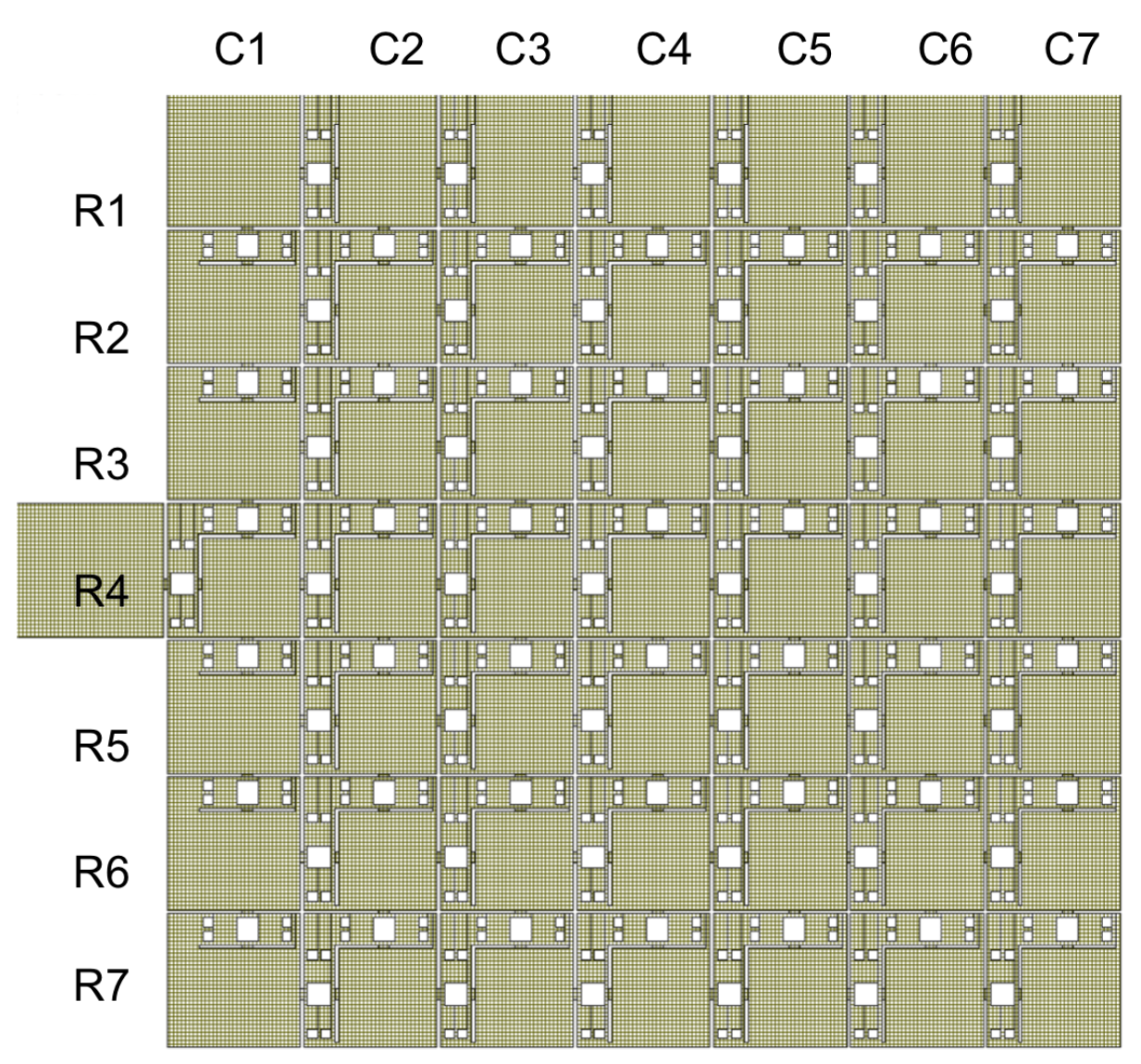
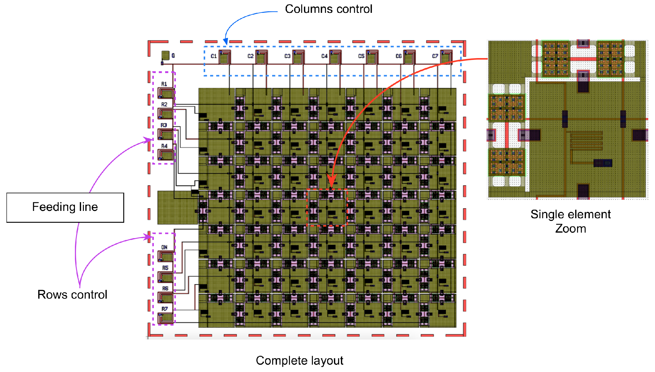
Another big advantage of this structure is that all the components can be fabricated directly on the substrate, power consumption is very low since MEMs are voltages driven, no current is required for their activation, and moreover, they can operate from low frequency up to 100 G H z . The main drawback of the reconfigurable structure is the complexity of the switch control network. The following Figure 3 shows the whole cad of a 7 × 7 matrix structure, with MEMs switches and control pins aimed at activate rows and columns of gold patches. The cad has been obtained with the professional software cadence. In the following, we’ll consider the 7 × 7 matrix as a basic structure since it can be combined with similar ones to obtain more complex geometries. The next section will detail a prototype fabrication of a reconfigurable matrix.

3. Development of a 7x7 Reconfigurable Matrix Structure Prototype

As a proof of concept in this section, a 7 × 7 reconfigurable matrix structure is described, designed, fabricated, numerically and experimentally assessed. As stated above one of the main prototype key of force is its monolithic structure, all the components are made with a single technology and in a single chip. This section is divided into two subsections: the first focuses on the MEMS switch, and the second on the whole matrix structure providing fabrication details.

3.1. MEMs Switches Design

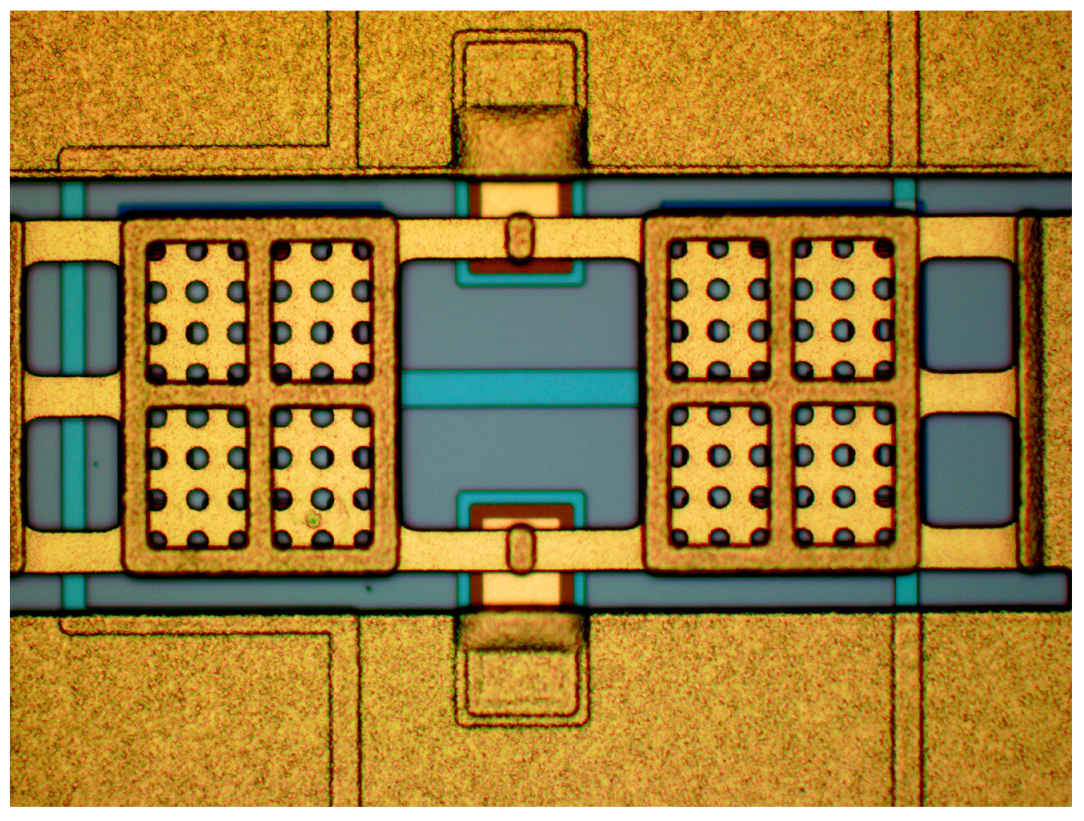
This subsection describes the RF-MEMS switches design and the key components to enable the reconfigurability of the proposed matrix reconfigurable structure. In particular, the following description is a summary for further additional and more detailed considerations about the MEMs design and characterization can be found in [44]. The considered switch device is a clamped-clamped structure of series ohmic type, driven by an electrostatic actuation mechanism. The series connection between the two interrupted sections of the main RF signal line is obtained utilizing an ohmic metal-to-metal contact between a movable membrane and the underlying contact pads. Figure 4 reports the MEMS switch fabricated prototype.
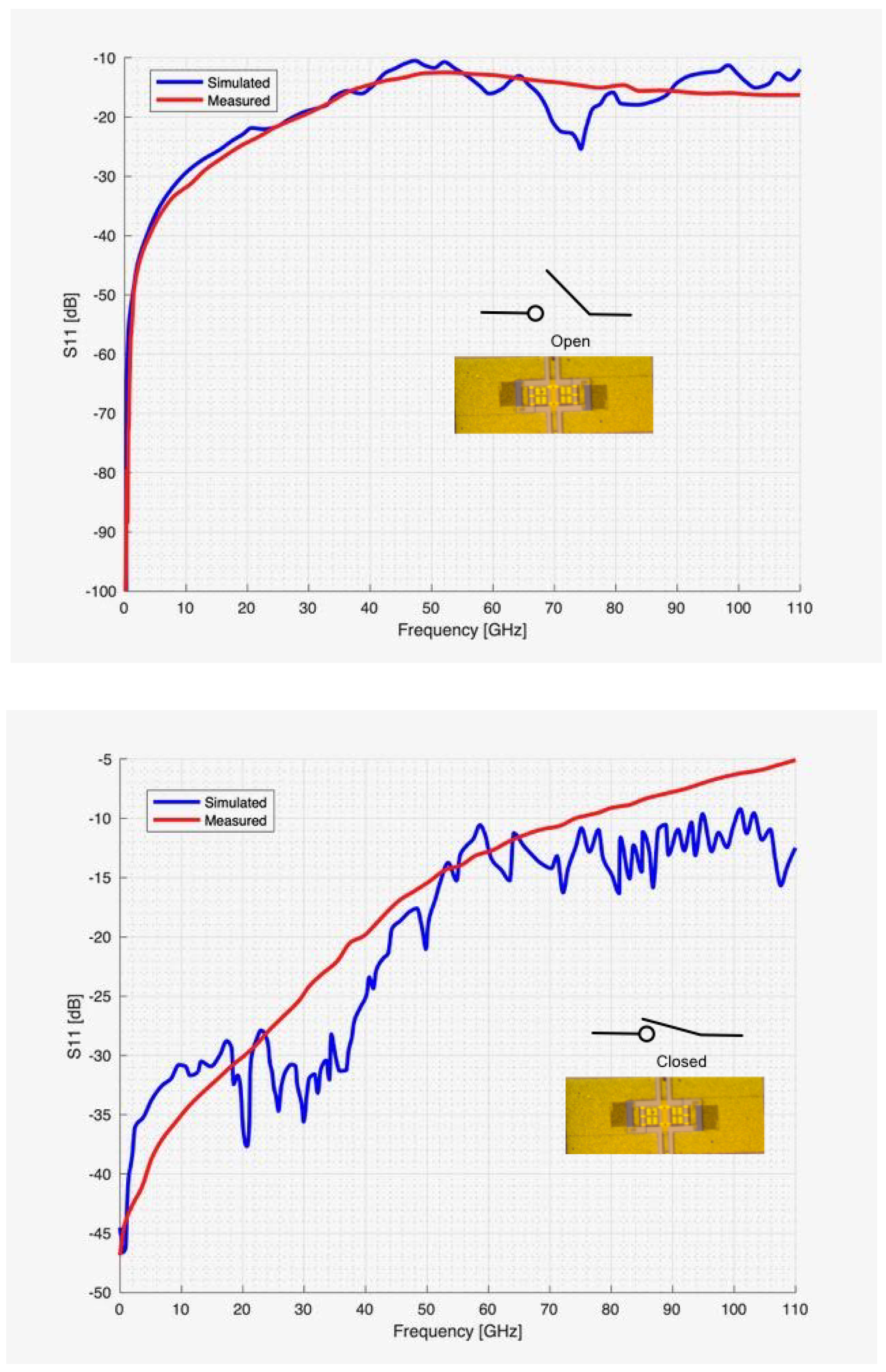
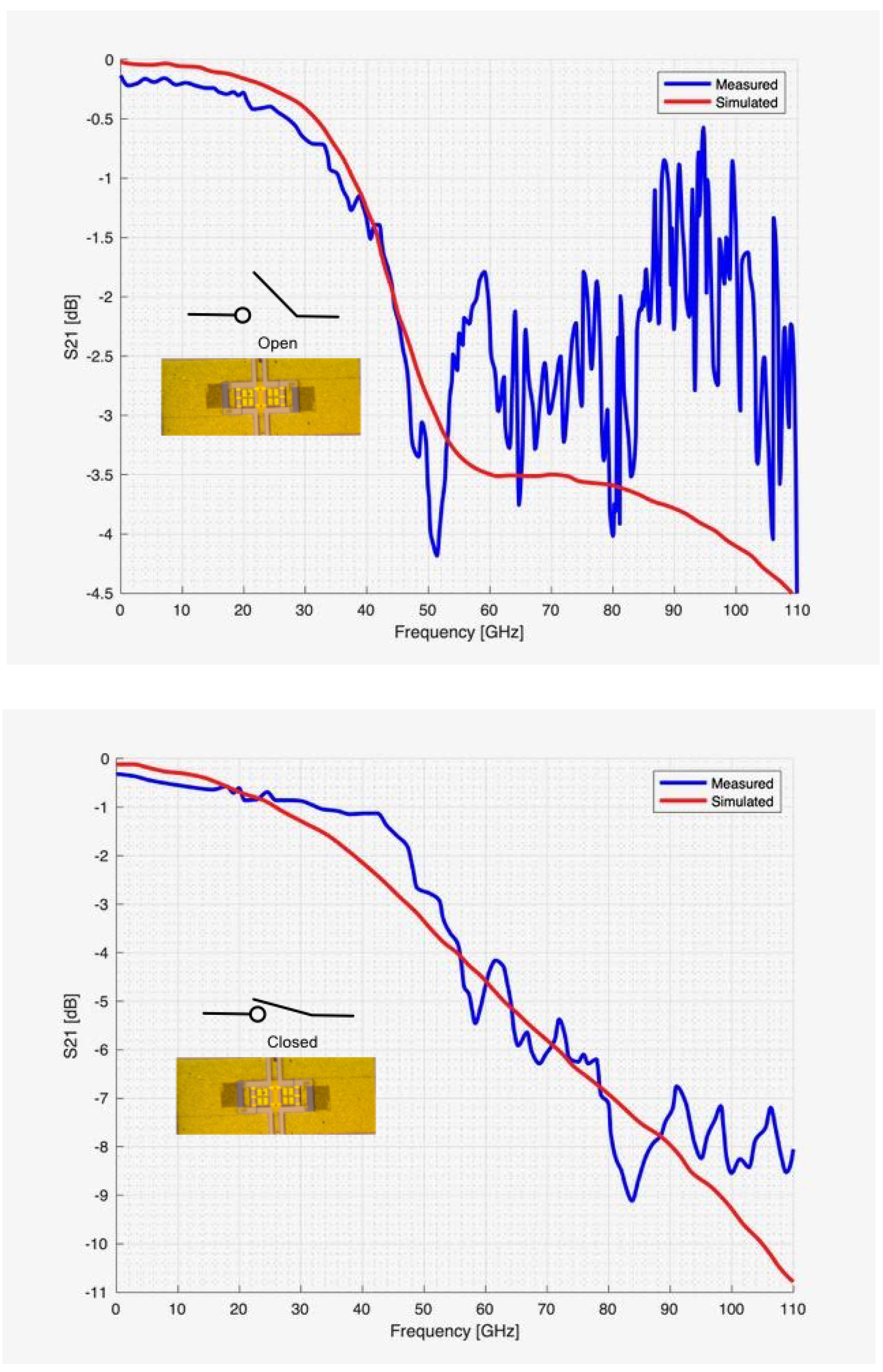
The switch dimensions are quite compact, with an overall reduced physical footprint of 430 × 170 μ m 2 . The switch layout reported in Figure 4 consists of an 8-mask surface micro-machining process developed on a 6-inch Silicon support, covered by a basic layer of Silicon oxide. The Silicon oxide is deposited and used on the different layers, to isolate them. Then, it is etched and filled with conductive materials, and an electrical connection must be established between adjacent layers. The fabrication procedure is detailed in [45,49]; more details concerning the different masks will be summarized in the following subsection to describe the reconfigurable matrix prototype. The scattering parameters (S-parameter) of the considered MEMS switch have been numerically and experimentally assessed. In particular, a comparison between simulated results obtained with commercial software, namely Ansys HFSS, and measurements have been performed with a vectorial network analyser (VNA) on a broad observation range starting from DC up to 110 GHz. In particular, the on-wafer measurement setup, the MEMS switch prototype, has been characterized using Ground-Signal-Ground (GSG) probes connected to a Vector Network Analyzer (VNA).
In particular, Figure 5 report the return loss S 11 in (a) open (when the membrane is in rest position) and (b) closed (pulled in membrane) conditions, respectively. The insertion loss S 21 is reported in Figure 6 also in this case in (a) open and (b) closed switch conditions, respectively. As it can be observed from the data reported in Figure 5 and Figure 6, the agreement between numerical and experimental results is very good. The overall measured return and insertion loss are quite good, especially up to 50GHz, at higher frequency bands, the performances of such switches are very satisfactory, and they outperform other electronic switches such as PIN diode or MOSFET transistors. In light of the considerations and experimental assessment, the RF-MEMS switch proved to be a compact and reliability-oriented device. It provides wideband and remarkable electrical features that make it a suitable building block for the proposed reconfigurable matrix structure.

3.2. 7 × 7 Matrix Prototype Description

In this subsection the description of 7 × 7 reconfigurable prototype is detailed. The complete CAD layout obtained with the Cadence software is reported in Figure 7. As stated above, one of the main advantages of this technology is that every component (gold patches, switches, feeding and control lines) can be designed on the same substrate and the final prototype, once completed and printed is immediately operative. The fabrication consists of eight different masks (the same procedure used for the production of the MEMs switches).
The first mask is used to realize the central buried electrode (in pink with reference of Figure 7) and the serpentine-shaped resistors connecting the movable membrane to the ground planes, and the lines laying under the anchoring points of the metallic bridge. It consists of a Poly-Silicon layer. In particular, the former are meant to keep the MEMs switches membrane to null voltage while preventing the RF signal from flowing towards the ground. The second mask extends the device’s reliability by acting as a micro-heaters and restoring the membrane to the rest position in case of stiction. Stiction is the missed release of the membrane when the voltage of the buried electrode is set to zero, and it occurs because of micro welding or trapped charge within the oxide since the voltage applied to the two pads implies a flow of current along the resistor, which results in a thermal expansion of the locked membrane and in an induced restoring force [43]. The third mask consists of a Multi-Metal layer based on Aluminium composing the buried sections of the RF underpass signal line (in blue with reference to Figure 7). It ends in correspondence of two contact pads laying on the surface of Silicon oxide, obtained by evaporating Gold (fifth mask). The suspended membrane provides the interrupted electrical connection of the signal lines, which is deployed onto a photoresist sacrificial layer (sixth mask). Then, two layers of electroplated Gold (seventh and eighth masks) compose the connection frames, the movable membrane (in brown), and the two anchoring points. The MEMS membranes’ nominal actuation (pull-in) is obtained with a voltage signal at 21V, which is the amount of voltage at which the membrane would reach its maximum displacement of about 2.5 μ m . Further details concerning the fabrication procedure and the stress residual estimation of the thin films are reported in [50,51].
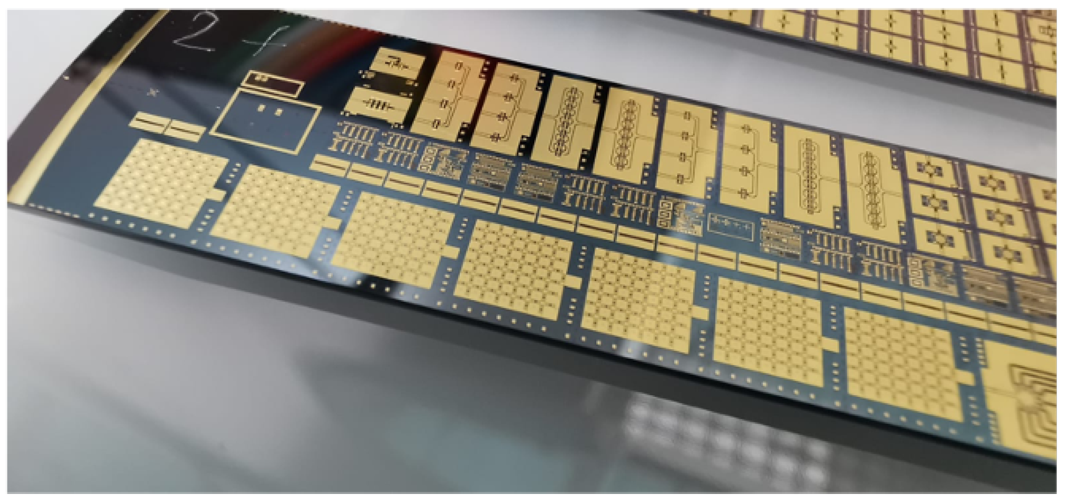
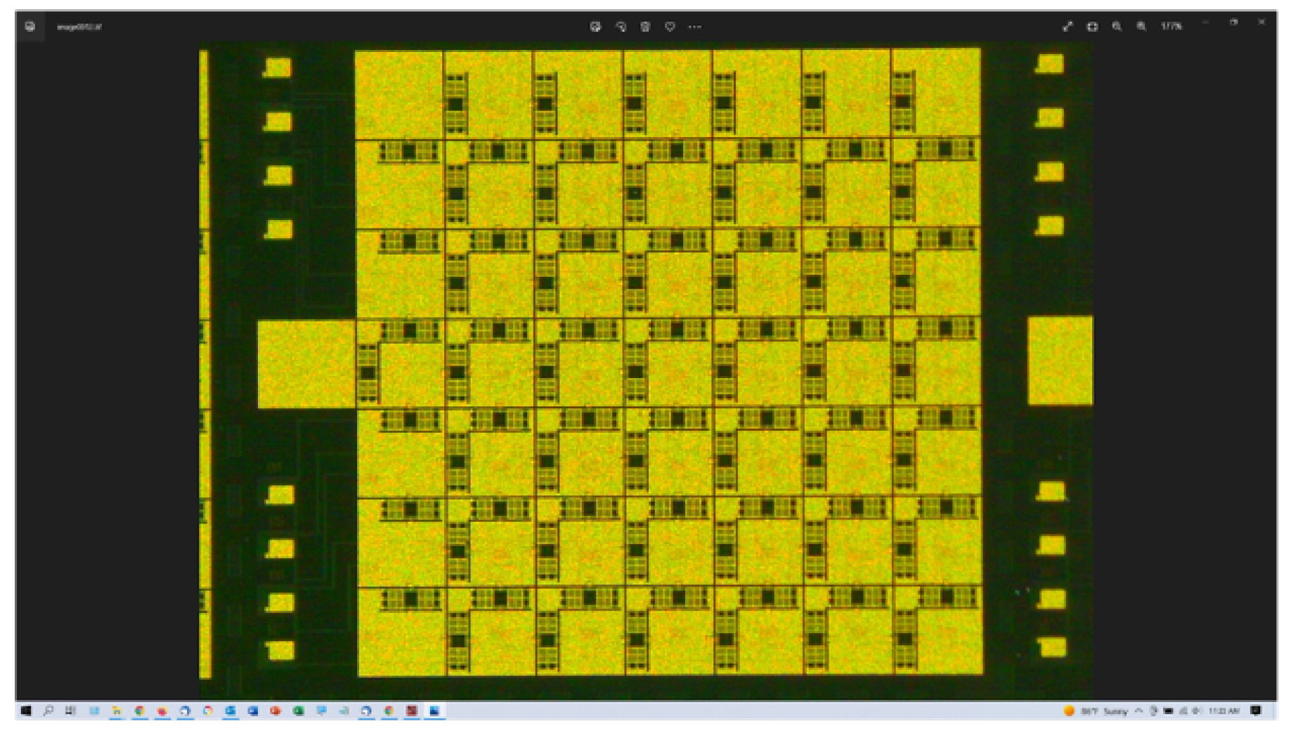
Figure 8 shows a photo of the Si wafer with different prototypes, while Figure 9 reports a high-resolution photo of a single prototype obtained with an optical microscope. The whole dimensions of the prototype are 5230 × 5230 μ m 2 . Each gold patch is 430 × 430 μ m 2 , and it is connected with the other surrounding patches by four MEMs switches. On the left side of Figure 9, it can be observed the gold pad is used as a feeding point for the RF signal. The prototype structure presents a thickness t = 656.4 μ m , more in detail: the gold layer has a thickness t g = 5 μ m , the silicon dioxide is characterized by a thickness t d i o x = 1.4 μ m and a dielectric permittivity ε d i o x = 3.94 , and the last layer made of silicon has a thickness t S i = 650 μ m and a dielectric permittivity ε S i = 11.9 . A matrix prototype have been cut from the Si wafer and predisposed for the experimental assessment.

4. Numerical and Experimental Assessment

In this section the numerical and experimental assessment of the obtained prototype is carried out in order to demonstrate the effectiveness of the proposed structure.

4.1. Numerical Assessment

Let us start with the first experiment, the matrix has been set as microstrip line of different width by activating rows of the matrix. In particular, we increased the microstrip width by adding different rows. The simulation was carried out using the ADS electromagnetic simulator (from Keysight company). The whole cad structure has been imported into the simulator, and for the sake of accuracy, the disconnected gold patches (with the surrounding MEMs switches in an open state) are considered in the simulation. In the first simulation, only one activated row is considered. This configuration which represents a microstrip of thickness t m = 430 μ m with an impedance of about Z m = 54.75 Ω . Then different rows have been added by properly activating the MEMs switch (up to six rows) in order to increase the microstrip width and consequently decrease the microstrip impedance. The microstrip width ranges from t m = 430 μ m up to t m = 3430 μ m . The obtained results are summarized in Table 1; the fourth column reports the microstrip impedance; as expected, the microstrip impedance decreases with the width starting from Z m = 54.75 Ω for a single activated row, and for six activated rows, the impedance decrease up to Z m = 10.34 Ω . Despite the simplicity of this first set of experiments, it is worth noticing that the capability to implement microstrip segments with different widths permits the fabrication of quarter wavelength transformers, broadband impedances transformers and other fundamental radio frequency or microwave components.
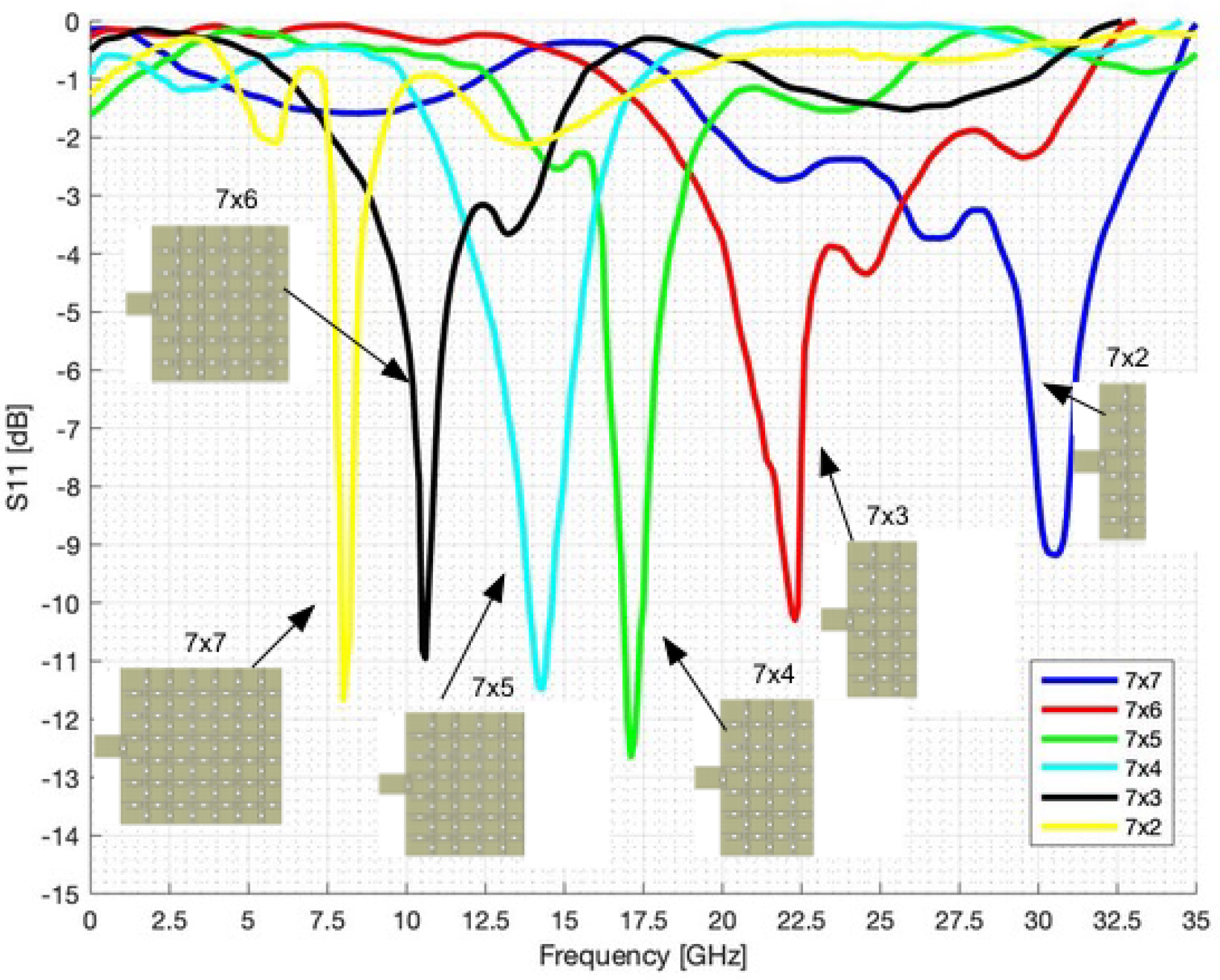
In the second set of numerical experiments, a more complex geometry consisting of a reconfigurable patch antenna has been considered. In these experiments, different columns are activated in order to modify the length and, consequently, the resonance frequency of a rectangular patch antenna, obtaining an electronic reconfigurable antenna able to operate in different frequency bands. The simulations were done with the ADS software, and also, in this case, to simulate realistic scenarios, the disconnected gold patches (with all the surrounding MEMS in an open state) were considered in the simulation. The obtained results are reported in Figure 10. As it can be noticed from the data reported in Figure 10 the patch obtained with all the seven columns activated represents a 5230 × 5230 μ m 2 square patch antenna with a resonance frequency of about f 7 × 7 = 8.0 G H z as indicated by the yellow curve of Figure 10. Then, as can be observed by reducing the column number from seven to two, the resonance frequency decreases consequently due to the antenna length reduction. The following resonance frequencies, with reference to Figure 10 have been obtained for the different configuration: f 7 × 6 = 10.5 G H z (black line), f 7 × 5 = 14.5 G H z (cyan line), f 7 × 4 = 17.0 G H z (green line), f 7 × 3 = 22.5 G H z (blue line), and f 7 × 3 = 30.0 G H z (red line).

4.2. Experimental Assessment

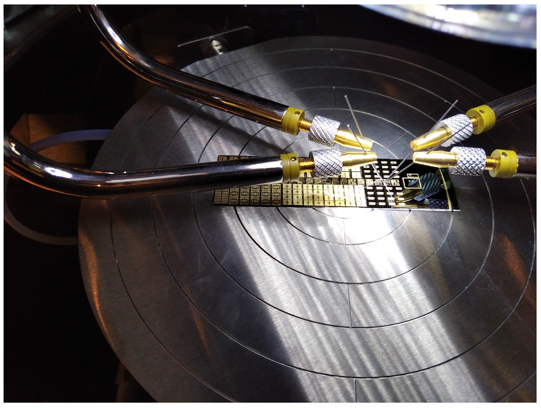
Concerning the scattering parameters, a set of on-wafer measurements has been carried out. The experimental setup is reported in Figure 11. The prototype has been characterized through Ground-Signal-Ground (GSG) probes connected to a Vector Network Analyser (VNA). A gold ground plane of thickness t g = 100 μ m has been placed below the prototype structure. The first set of measurements aims to measure the impedance of microstrip lines of different widths obtained by activating rows of the matrix as in the first numerical experiment. The goal of this first set of measures is to confirm the simulated data reported in Table 1. The comparisons between numerical and experimental results are summarized in the following Table 2, as it can be noticed the measurements are in good agreement with the simulation, and the maximum error is 11.0%. The error is probably due to the measurement procedure that used small needles to connect the prototype sections. However, the results obtained can be considered quite satisfactory.
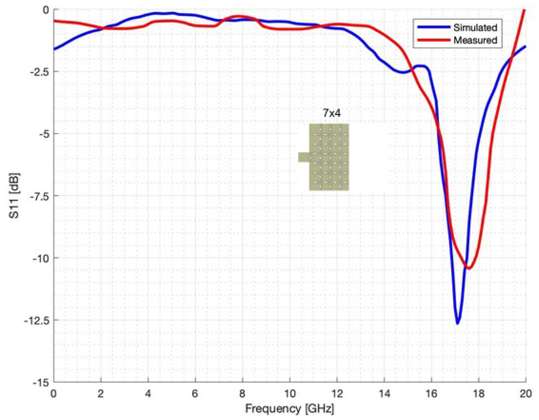
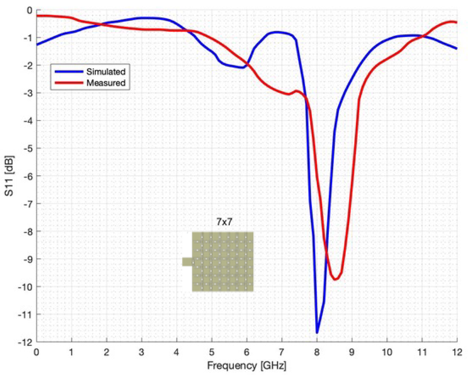
The next set of measures aims to verify the prototype’s capabilities as a reconfigurable patch antenna. The structure has been set as a rectangular antenna patch by activating four of the seven columns characterized by a resonance frequency f 7 × 4 = 17.0 G H z . The patch antenna’s S 11 has been measured with the vectorial network analyser and considering the experimental measurement setup shown in Figure 11. The results are reported and compared with the numerical data in Figure 12, as it can be noticed the measured resonance frequency is f m = 17.5 G H z 500 MHz higher with respect to the simulated data. The frequency shift is probably due to the considered experimental measurement setup, since the connection between VNA and patch antenna has been done with suitable conductive tips as shown in Figure 11. The next measure considers the structure with all the seven columns activated, corresponding to a square patch of dimension 5230 × 5230 μ m 2 and a resonance frequency of f 7 × 7 = 8.0 G H z . Also, in this case, the measures are compared with the numerical data and reported in Figure 12. Also, in this case, the measured resonance f 7 × 7 = 8.6 G H z , 600 MHz higher with respect to the simulated data. A similar frequency shift has been observed for all the other configurations.

5. Conclusion

This paper presents a reconfigurable structure that can be set by modifying its geometry to be a reconfigurable antenna or microwave component. The structure works like a field-programmable gate array (FPGA), a configurable integrated circuit that can be repeatedly programmed after manufacturing. It consists of an array of square gold blocks with a connecting set of electronic MEMS switches. The gold blocks can be configured to interconnect each other to perform various radio frequency or microwave components, such as frequency reconfigurable antennas, impedance transformers and other basic RF components. As a proof of concept, an experimental prototype consisting of 7*7 gold patches interconnected by means of a set of RF-MEMS switches is designed, fabricated, numerically and experimentally assessed. The proposed programmable prototype is an attractive candidate for modern wireless communications such as mm-wave devices and CubeSat satellites. The obtained results have shown the potential versatility of the proposed reconfigurable structure. Future advances will be devoted to increasing the dimensions and number of patch elements and simplifying the control structure of the MEM switches.

Author Contributions

For research article Conceptualization, Jacopo Iannacci and Massimo Donelli; methodology, Massimo Donelli and Mohammedhusen Manekiya; software, Massimo Donelli and Mohammedhusen Manekiya; validation, Massimo Donelli and Mohammedhusen Manekiya; formal analysis, Massimo Donelli and Mohammedhusen Manekiya; investigation, Massimo Donelli and Mohammedhusen Manekiya; resources, Massimo Donelli and Mohammedhusen Manekiya; data curation, Jacopo Iannacci; writing—original draft preparation, Massimo Donelli; writing—review and editing, Massimo Donelli, Mohammedhusen Manekiya, and Jacopo Iannacci ; visualization, Massimo Donelli, Mohammedhusen Manekiya, and Jacopo Iannacci; supervision, Massimo Donelli; project administration, Massimo Donelli and Jacopo Iannacci; All authors have read and agreed to the published version of the manuscript.

Acknowledgments

The authors would like to thank Dr. E. Bortolotti for the revision of the manuscript.

Conflicts of Interest

The authors declare no conflicts of interest.The funders had no role in the design of the study; in the collection, analyses, or interpretation of data; in the writing of the manuscript; or in the decision to publish the results.

References

  1. M. Poulakis, “6G’s Metamaterials Solution: There’s plenty of bandwidth available if we use reconfigurable intelligent surfaces,” IEEE Spectr., vol. 59, no. 11, pp. 40–45, Nov. 2022. [CrossRef]
  2. C. A. Balanis and P. I. Ioannides, Introduction to Smart Antennas. in Synthesis Lectures on Antennas. Cham: Springer International Publishing, 2007. [CrossRef]
  3. M. A. Matin, Ed., Wideband, Multiband, and Smart Antenna Systems. in Signals and Communication Technology. Cham: Springer International Publishing, 2021. [CrossRef]
  4. R. C. Hansen, Phased array antennas, 2nd ed. in Wiley series in microwave and optical engineering. Hoboken, N.J: Wiley, 2009.
  5. S. Applebaum, “Adaptive arrays,” IEEE Trans. Antennas Propagat., vol. 24, no. 5, pp. 585–598, Sep. 1976. [CrossRef]
  6. Shiann-Jeng Yu and Ju-Hong Lee, “Adaptive array beamforming based on an efficient technique,” IEEE Trans. Antennas Propagat., vol. 44, no. 8, pp. 1094–1101, Aug. 1996. [CrossRef]
  7. F. J. Ares-Pena, J. A. Rodriguez-Gonzalez, E. Villanueva-Lopez, and S. R. Rengarajan, “Genetic algorithms in the design and optimization of antenna array patterns,” IEEE Trans. Antennas Propagat., vol. 47, no. 3, pp. 506–510, Mar. 1999. [CrossRef]
  8. A. Massa, M. Donelli, F. G. B. DeNatale, S. Caorsi, and A. Lommi, “Planar Antenna Array Control With Genetic Algorithms and Adaptive Array Theory,” IEEE Trans. Antennas Propagat., vol. 52, no. 11, pp. 2919–2924, Nov. 2004. [CrossRef]
  9. S. H. Son, S. Y. Eom, S. I. Jeon, and W. Hwang, “Automatic Phase Correction of Phased Array Antennas by a Genetic Algorithm,” IEEE Trans. Antennas Propagat., vol. 56, no. 8, pp. 2751–2754, Aug. 2008. [CrossRef]
  10. M. Donelli, R. Azaro, F. G. B. DeNatale, and A. Massa, “An Innovative Computational Approach Based on a Particle Swarm Strategy for Adaptive Phased-Arrays Control,” IEEE Trans. Antennas Propagat., vol. 54, no. 3, pp. 888–898, Mar. 2006. [CrossRef]
  11. M. Donelli, A. Martini, and A. Massa, “A Hybrid Approach Based on PSO and Hadamard Difference Sets for the Synthesis of Square Thinned Arrays,” IEEE Trans. Antennas Propagat., vol. 57, no. 8, pp. 2491–2495, Aug. 2009. [CrossRef]
  12. M. Behera, A. B. Sahoo, H. Pradhan, and B. B. Mangaraj, “Performance comparison of PSO optimized mutually coupled linear array antenna with Yagi-Uda antenna,” in 2013 IEEE CONFERENCE ON INFORMATION AND COMMUNICATION TECHNOLOGIES, Thuckalay, Tamil Nadu, India: IEEE, Apr. 2013, pp. 718–723. [CrossRef]
  13. S. I. M. Sheikh et al., “Analog/Digital Ferrite Phase Shifter for Phased Array Antennas,” Antennas Wirel. Propag. Lett., vol. 9, pp. 319–321. 2010. [CrossRef]
  14. J. S. Herd and M. D. Conway, “The Evolution to Modern Phased Array Architectures,” Proc. IEEE, vol. 104, no. 3, pp. 519–529, Mar. 2016. [CrossRef]
  15. B. T. Perry et al., “Low cost phased array radar for applications in engineering education,” in 2013 IEEE International Symposium on Phased Array Systems and Technology, Waltham, MA, USA: IEEE, Oct. 2013, pp. 416–420. [CrossRef]
  16. K. Gyoda and T. Ohira, “Design of electronically steerable passive array radiator (ESPAR) antennas,” in IEEE Antennas and Propagation Society International Symposium. Transmitting Waves of Progress to the Next Millennium. 2000 Digest. Held in conjunction with: USNC/URSI National Radio Science Meeting (Cat. No.00CH37118), Salt Lake City, UT, USA: IEEE, 2000, pp. 922–925. [CrossRef]
  17. M. D. Migliore, D. Pinchera, and F. Schettino, “A simple and robust adaptive parasitic antenna,” IEEE Trans. Antennas Propagat., vol. 53, no. 10, pp. 3262–3272, Oct. 2005. [CrossRef]
  18. P. Rocca, M. Donelli, G. Oliveri, F. Viani, and A. Massa, “Reconfigurable sum–difference pattern by means of parasitic elements for forward-looking monopulse radar,” IET Radar, Sonar & amp; Navigation, vol. 7, no. 7, pp. 747–754, Aug. 2013. [CrossRef]
  19. S. Raman, P. Mohanan, N. Timmons, and J. Morrison, “Microstrip-Fed Pattern- and Polarization- Reconfigurable Compact Truncated Monopole Antenna,” Antennas Wirel. Propag. Lett., vol. 12, pp. 2013. [CrossRef]
  20. Z. Qu, J. R. Kelly, Z. Wang, S. Alkaraki, and Y. Gao, “A Reconfigurable Microstrip Patch Antenna With Switchable Liquid-Metal Ground Plane,” Antennas Wirel. Propag. Lett., vol. 22, no. 5, pp. 1045–1049, May 2023. [CrossRef]
  21. J. Wang, V. Manohar, and Y. Rahmat-Samii, “K-Band Circularly Polarized Beam Steerable Reflectarray Enabling Internet of Space: Conceptualization and Validation,” IEEE Trans. Antennas Propagat., vol. 70, no. 8, pp. 6703–6717, Aug. 2022. [CrossRef]
  22. J. Huang, M. Shirazi, and X. Gong, “A New Arraying Technique for Band-Switchable and Polarization-Reconfigurable Antenna Arrays With Wide Bandwidth,” IEEE Open J. Antennas Propag., vol. 3, pp. 1025–1040, 2022. [CrossRef]
  23. E. Carrasco, M. Barba, and J. A. Encinar, “X-Band Reflectarray Antenna With Switching-Beam Using PIN Diodes and Gathered Elements,” IEEE Trans. Antennas Propagat., vol. 60, no. 12, pp. 5700–5708, Dec. 2012. [CrossRef]
  24. A. Wahab and J. Xu, “U-slot Circular Patch Antenna for WLAN Application,” TELKOMNIKA, vol. 14, no. 2, pp. 323–328, May 2015. [CrossRef]
  25. Youngje Sung, “Investigation Into the Polarization of Asymmetrical- Feed Triangular Microstrip Antennas and its Application to Reconfigurable Antennas,” IEEE Trans. Antennas Propagat., vol. 58, no. 4, pp. 1039–1046, Apr. 2010. [CrossRef]
  26. G. Rebeiz et al., “Tuning in to RF MEMS,” IEEE Microwave, vol. 10, no. 6, pp. 55–72, Oct. 2009. [CrossRef]
  27. M. S. Nishamol, V. P. Sarin, D. Tony, C. K. Aanandan, P. Mohanan, and K. Vasudevan, “An Electronically Reconfigurable Microstrip Antenna With Switchable Slots for Polarization Diversity,” IEEE Trans. Antennas Propagat., vol. 59, no. 9, pp. 3424–3427, Sep. 2011. [CrossRef]
  28. S. W. Lee and Y. Sung, “Compact Frequency Reconfigurable Antenna for LTE/WWAN Mobile Handset Applications,” IEEE Trans. Antennas Propagat., vol. 63, no. 10, pp. 4572–4577, Oct. 2015. [CrossRef]
  29. Chao Sun, Huili Zheng, Lingfei Zhang, and Ying Liu, “A Compact Frequency-Reconfigurable Patch Antenna for Beidou (COMPASS) Navigation System,” Antennas Wirel. Propag. Lett., vol. 13, pp. 967–970. 2014. [CrossRef]
  30. D. Sanchez-Escuderos, M. Ferrando-Bataller, M. Baquero-Escudero, and J. I. Herranz, “Reconfigurable Slot-Array Antenna With RF-MEMS,” Antennas Wirel. Propag. Lett., vol. 10, pp. 721–725. 2011. [CrossRef]
  31. T. Debogovic and J. Perruisseau-Carrier, “Low Loss MEMS-Reconfigurable 1-Bit Reflectarray Cell With Dual-Linear Polarization,” IEEE Trans. Antennas Propagat., vol. 62, no. 10, pp. 5055–5060, Oct. 2014. [CrossRef]
  32. Wenquan Cao, Bangning Zhang, Aijun Liu, Tongbin Yu, Daosheng Guo, and Kegang Pan, “A Reconfigurable Microstrip Antenna With Radiation Pattern Selectivity and Polarization Diversity,” Antennas Wirel. Propag. Lett., vol. 11, pp. 453–456. 2012. [CrossRef]
  33. M. Shirazi, J. Huang, T. Li, and X. Gong, “A Switchable-Frequency Slot-Ring Antenna Element for Designing a Reconfigurable Array,” Antennas Wirel. Propag. Lett., vol. 17, no. 2, pp. 229–233, Feb. 2018. [CrossRef]
  34. D. F. Macedo, D. Guedes, L. F. M. Vieira, M. A. M. Vieira, and M. Nogueira, “Programmable Networks—From Software-Defined Radio to Software-Defined Networking,” IEEE Commun. Surv. Tutorials, vol. 17, no. 2, pp. 1102–1125, 2015. [CrossRef]
  35. A. Kaiser, "The potential of MEMS components for re-configurable RF interfaces in mobile communication terminals," in Proc. ESSCIRC. Villach Austria, 2001, pp. 25-28.
  36. G. M. Rebeiz, RF-MEMS: Theory Design, and Technology, 1st ed. Hoboken, NJ USA: Wiley, 2003 pp. 1-512.
  37. A. Ocera, P. Farinelli, P. Mezzanotte, R. Sorrentino, B. Margesin, and F. Giacomozzi, “A Novel MEMS-Tunable Hairpin Line Filter on Silicon Substrate,” in 2006 European Microwave Conference, Manchester, UK, Sep. 2006, pp. 803–806. [CrossRef]
  38. Ker Chia Lee, Hieng Tiong Su, and M. K. Haldar, “Performance of a configurable microstrip filter using triple mode resonator and RF-MEMS switches,” in 2010 IEEE Asia-Pacific Conference on Applied Electromagnetics (APACE), Port Dickson, Nov. 2010, pp. 1–4. [CrossRef]
  39. F. Gentili, L. Pelliccia, F. Cacciamani, P. Farinelli, and R. Sorrentino, “RF -MEMS bandwidth-reconfigurable hairpin filters,” in 2012 Asia Pacific Microwave Conference Proceedings, Kaohsiung, Taiwan, Dec. 2012, pp. 735–737. [CrossRef]
  40. R. R. Mansour, “RF-MEMS for space applications,” in 2005 International Conference on MEMS,NANO and Smart Systems, Banff, AB, Canada, 2005, pp. 191–192. [CrossRef]
  41. J. Iannacci et al., “RF-MEMS for 5G mobile communications: A basic attenuator module demonstrated up to 50 GHz,” in 2016 IEEE SENSORS, Orlando, FL, USA, Oct. 2016, pp. 1–3. [CrossRef]
  42. J. Iannacci, A. Faes, F. Mastri, D. Masotti, V. Rizzoli, “A MEMS-Based Wide-Band Multi- State Power Attenuator for Radio Frequency and Microwave Applications,” Proc. of TechConnect World, NSTI-Nanotech 2010, pp. 328-331, Jun. 2010.
  43. J. Iannacci, D. Masotti, T. Kuenzig, M. Niessner, “A reconfigurable impedance matching network entirely manufactured in RF- MEMS technology, ” Proc. of SPIE, vol. 8066, pp. 1-12, Apr. 2011.
  44. J. Iannacci, M. Huhn, C. Tschoban, H. Potter, “RF-MEMS Technology for 5G: Series and Shunt Attenuator Modules Demonstrated up to 110 GHz,” IEEE EDL, vol. 37, no. 10, pp. 1336-1339, Oct. 2016.
  45. J. Iannacci, M. Huhn, C. Tschoban, H. Potter, “RF-MEMS Technology for future (5G) mobile and high frequency applications: reconfigurable 8-bit power attenuator tested up to 110 GHz” IEEE EDL, vol. 37, no. 12, pp. 1646-1649, Dec. 2016.
  46. M. Donelli, M. Manekiya, and J. Iannacci, “Broadband MST sensor probes based on a SP3T MEMS switch,” in 2019 IEEE International Symposium on Antennas and Propagation and USNC-URSI Radio Science Meeting, Atlanta, GA, USA, Jul. 2019, pp. 649–650. [CrossRef]
  47. P.Ssejjuuko, M. Donelli, and J. Iannacci, "Exploiting RF-MEMS Switches for pattern reconfigurable parasitic antennas," 2021 Springer International Conference on Micro/Nanoelectronics Systems Tracks of MNDCS-2021, Assam, India, 2021, Jan. 29-31.
  48. E. Hammerstad and O. Jensen, “Accurate Models for Microstrip Computer-Aided Design,” in MTT-S International Microwave Symposium Digest, Washington, DC,USA, 1980, vol. 80, pp. 407–409. [CrossRef]
  49. J. Iannacci, Practical Guide to RF-MEMS, 1st ed. Wiley, 2013. [CrossRef]
  50. V. Mulloni, F. Giacomozzi, and B. Margesin, “Controlling stress and stress gradient during the release process in gold suspended micro-structures,” Sensors and Actuators A: Physical, vol. 162, no. 1, pp. 93–99, Jul. 2010. [CrossRef]
  51. M. N. Mollah and N. C. Karmakar, “RF-MEMS switches: paradigms of microwave switching,” in APMC 2001. 2001 Asia-Pacific Microwave Conference (Cat. No.01TH8577), Taipei, Taiwan: IEEE, 2001, pp. 1024–1027. [CrossRef]
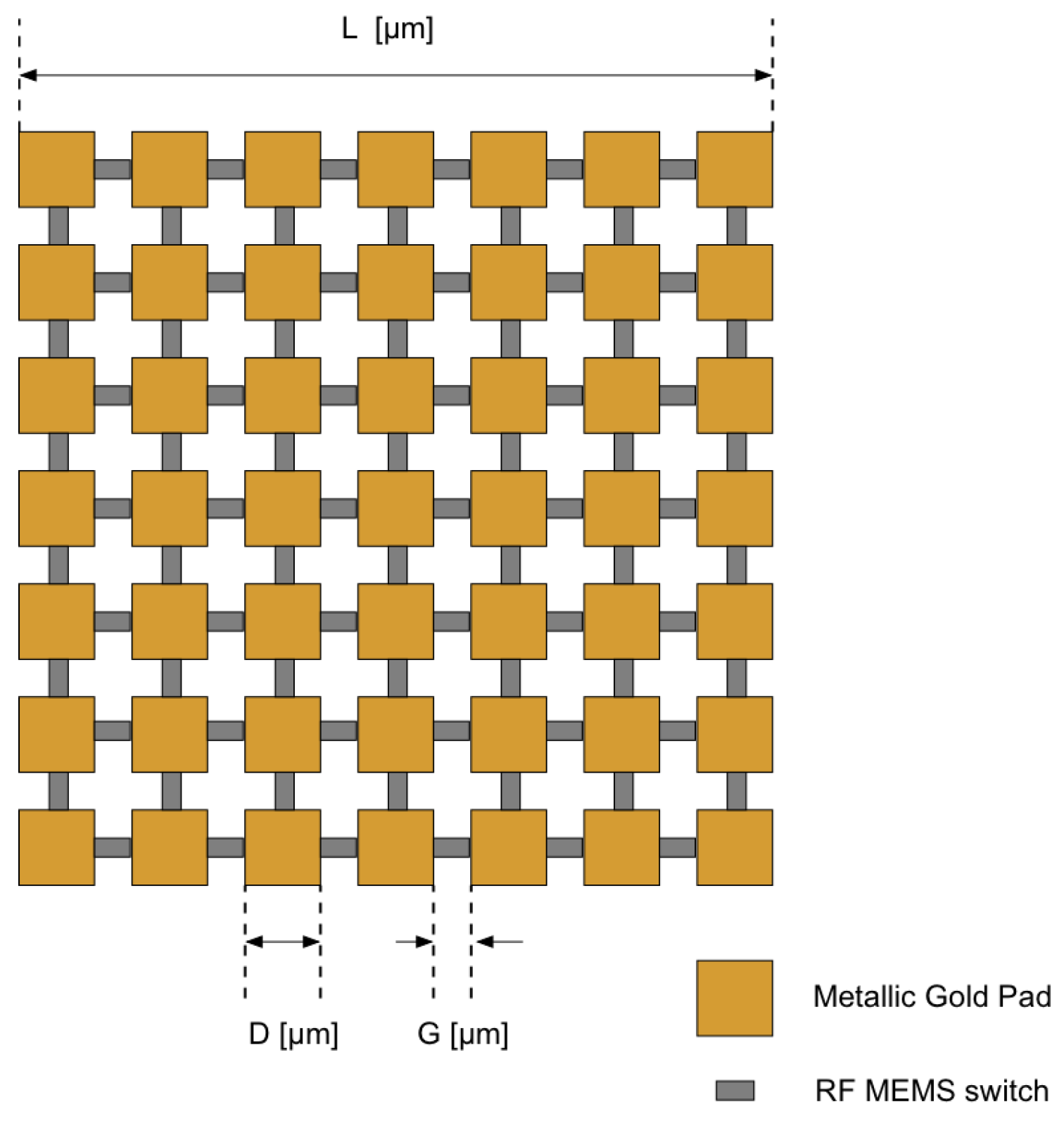
Figure 1. Schema of the reconfigurable antenna structure based on a matrix of RF-MEMS switches.
Preprints 116999 g001
Figure 2. Matrix configured as patch antenna equipped with a quarter wavelength transformer and feeding microstrip.
Preprints 116999 g002
Figure 3. CAD schema of a 7 × 7 elements reconfigurable matrix.
Preprints 116999 g003
Figure 4. Micro photo details of the single RF MEMS switch.
Preprints 116999 g004
Figure 5. RF-MEMS switch simulated vs. measured S 11 , (a) open, (b) closed position.
Preprints 116999 g005
Figure 6. RF-MEMS switch simulated vs. measured S 21 , (a) open, (b) closed position.
Preprints 116999 g006
Figure 7. Complete CAD layout of the 7 × 7 elements reconfigurable matrix, obtained with the Cadence software.
Preprints 116999 g007
Figure 8. Photo of the Si wafer with the obtained prototypes.
Preprints 116999 g008
Figure 9. High resolution photo of the 7 × 7 matrix prototype made with an optical microscope.
Preprints 116999 g009
Figure 10. Simulation of different rectangular antenna patches obtained by properly connects the gold pads.
Preprints 116999 g010
Figure 11. Photo of the experimental measurement setup.
Preprints 116999 g011
Figure 12. Simulated vs. experimental measurement for a 7 × 4 rectangular patch configuration.
Preprints 116999 g012
Figure 13. Simulated vs. experimental measurement for a 7 × 7 rectangular patch configuration.
Preprints 116999 g013
Table 1. Reconfigurable structure set as microstrip of different widths.
Rows Coloumns Thickness [ μ m ] Impedance [ Ω ]
1 7 430 54.75
2 7 1030 35.82
3 7 1630 25.42
4 7 2230 18.21
5 7 2830 12.68
6 7 3430 10.34
Table 2. Microstrip of different widths, simulation vs. mesures.
Thickness [ μ m ] Simulated [ Ω ] Measured [ Ω ] Error %
430 54.75 60.22 10.0
1030 35.82 38.68 8.0
1630 25.42 28.21 11.0
2230 18.21 19.81 8.8
2830 12.68 14.01 10.5
3430 10.34 11.30 9.3
Disclaimer/Publisher’s Note: The statements, opinions and data contained in all publications are solely those of the individual author(s) and contributor(s) and not of MDPI and/or the editor(s). MDPI and/or the editor(s) disclaim responsibility for any injury to people or property resulting from any ideas, methods, instructions or products referred to in the content.
Copyright: This open access article is published under a Creative Commons CC BY 4.0 license, which permit the free download, distribution, and reuse, provided that the author and preprint are cited in any reuse.
Prerpints.org logo

Preprints.org is a free preprint server supported by MDPI in Basel, Switzerland.

Subscribe

© 2024 MDPI (Basel, Switzerland) unless otherwise stated