1. Introduction
Born from four parents, molecular analysis, molecular biology, biodefence and , the field of microfluidics has always had a large potential to be disruptive in many different . With its foundation on basic principles of small liquid volume actuation aiming at the miniaturization of analytical and chemical , it held and still holds the promise of revolutionizing a plethora of different .
Especially over the last few years, the microfluidics industry has experienced exceptional growth. The industry with its many applications such as chemical analysis, point-of-care , pharmaceutical using for example microphysiological is expected to continue its growth at a compound annual growth rate of 2.2% until 2028 Regardless of the application, the internal geometry of a microfluidic circuit often plays a crucial role in the functionality of the device. For example, precisely required dilution ratios in point-of-care diagnostic devices or the need for physiologically relevant shear stresses in microphysiological can put tight geometrical constraints on chip manufacturers.
For something so important to the device’s functionality, the industry has an interest in being able to characterize the internal geometry of a chip. Chips are often made of multiple structured layers sealed on top of each other to form the final product. Dimension measurement of the structure before sealing is doable (for example by optical microscopy or stylus profilometry). However, once assembled the channels are on the inside of a chip, making their characterization more difficult due to material properties and physical constraints. This is a major issue, because the assembly method can change the structure of the chip compared to its unassembled state. This leaves the user as well as the manufacturer in the unknown regarding the geometry and dimensions of the flow circuit they are actually using or providing.
The industry itself has identified the lack of sensitive and standardized testing methods and as one of the major hurdles to overcome for it to fulfil its revolutionary .
To help the microfluidic industry overcome this challenge, this work presents multiple protocols for measuring the dimensions of internal microfluidic channels of fully assembled transparent chips. Each protocol’s reproducibility and precision are analyzed and compared against each other. Both glass and polymer chips are used as measuring substrates to identify the influence of material on the reproducibility of the results.
The protocols described herein will enable automated, non-destructive, reproducible characterization of internal geometry of transparent microfluidic chips after assembly, making them suitable for industrial applications. Thereby, they remove the uncertainty caused by any potential deformation during assembly, allowing users to be sure of the device they are using and manufacturers to be confident of the chips they are providing.
The article has the following structure: Firstly, the chip designs used as measurement substrates will be established. Then we elaborate on the different measuring techniques used and present their results. The different sets of results will be analyzed followed by consistency tests between the different protocols and between the protocols and nominal values. Ultimately, the influence of different material on the dimension measurements will be examined. A discussion and conclusions can be found at the end of the article.
2. Chips Geometries
Batches of chips were designed and manufactured out of two different materials; D263©bio glass17 and COC (Cyclic Olefin Copolymer, tradename TOPAS©18). The chips of each material have different internal dimensions and different designs. The choice of geometries was a consequence of the different applications for these chips in the EURAMET 20NRM02 MFMET (MFMET – Establishing Metrology Standards in Microfluidic ). These applications included most notably, leakage , flow resistivity , and the dimensional measurements described here.
All designs adhere to the ISO 22916:2022 standard on interoperability requirements for dimensions, connections and initial classification of microfluidic . Most notably influencing the chips’ footprint as well as connection positions and dimensions. This allowed the significant number of different participants to use the same connector and be sure that the chips were compatible with each and everyone’s measurement setup. In addition, these chips are meant to serve as transfer standards for other laboratories. Compliance with ISO 22916:2022 will facilitate compatibility with laboratories outside the scope of this project.
2.1. Glass Transfer Standart Chips
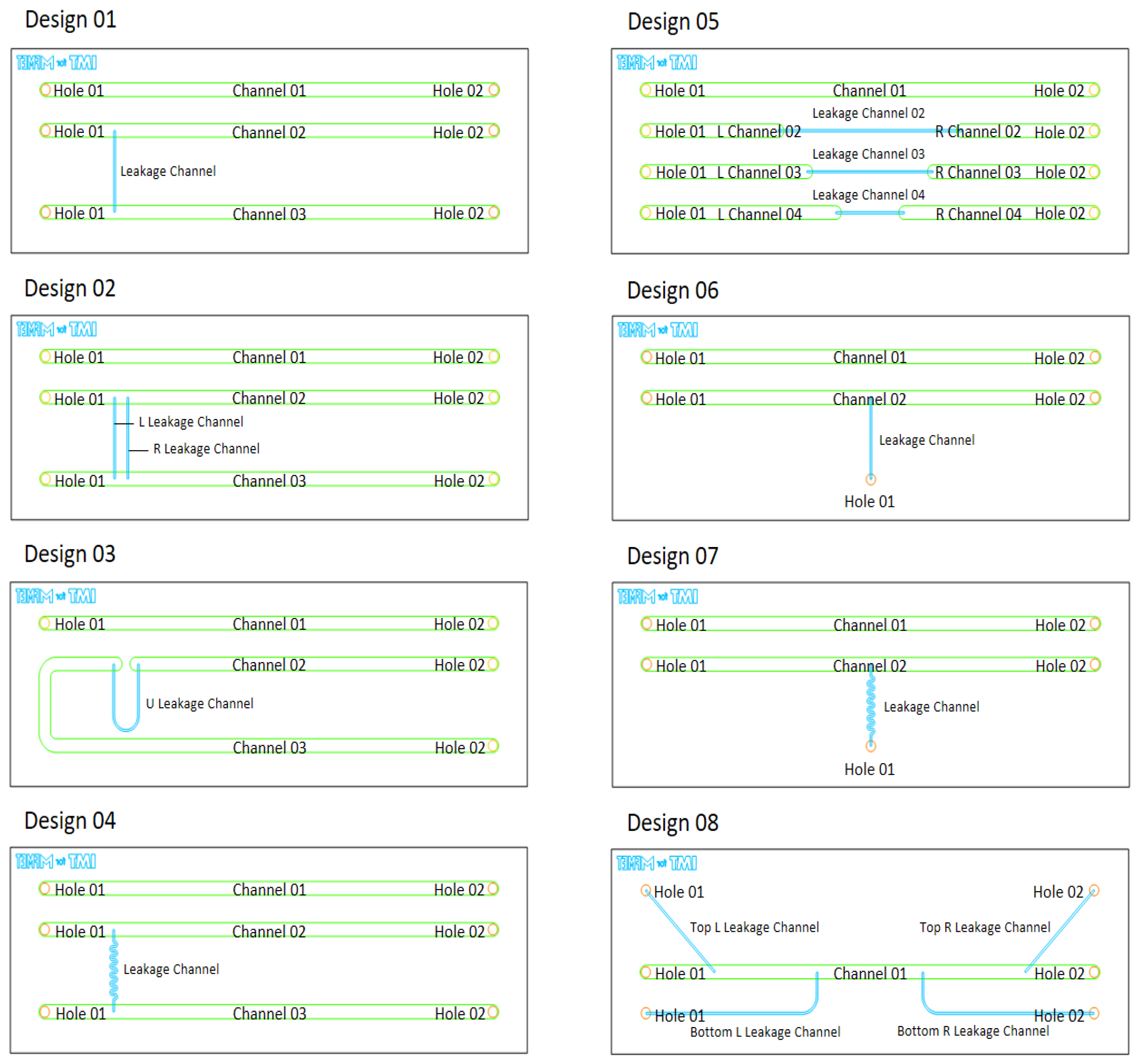
In glass, eight different chip designs (footprint 15 x 45 mm) were established (see
Figure 1). Each design has one or several main channels, some of which were connected to one or multiple so-called leakage channels: a channel significantly smaller in cross-section than the main channels, thus simulating a leak. All glass designs, except design 08, have a reference channel (Channel 01 in
Figure 1) that has no additional side issues to it.
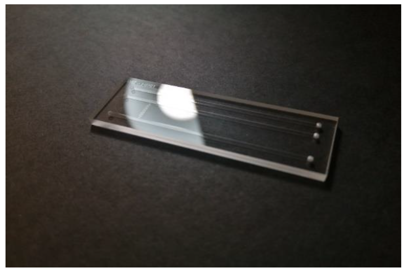
Figure 3 shows one of the glass Design 04 chips as an example. Technical design drawings of these glass transfer standard chips can be found in the Electronic Supplementary Information.
The glass chips were fabricated by IMT Masken und Teilungen AG, Switzerland, out of D263©bio using isotropic wet-etching techniques utilizing hydrofluoric acid-based etching solutions commonly used in the semiconductor industry. The final chips consist of two halves, which, after their individual fabrication, are bonded one on top of the other. The device’s critical dimensions passed quality assurance during and after processing. For design 01 to 05 four chips were produced, of design 06 and 07 three chips and of design 08 a two were fabricated. One of each was kept apart from this study as a back-up.
Figure 1.
Different glass chip designs and their geometry nomenclature for measurements.
Figure 1.
Different glass chip designs and their geometry nomenclature for measurements.
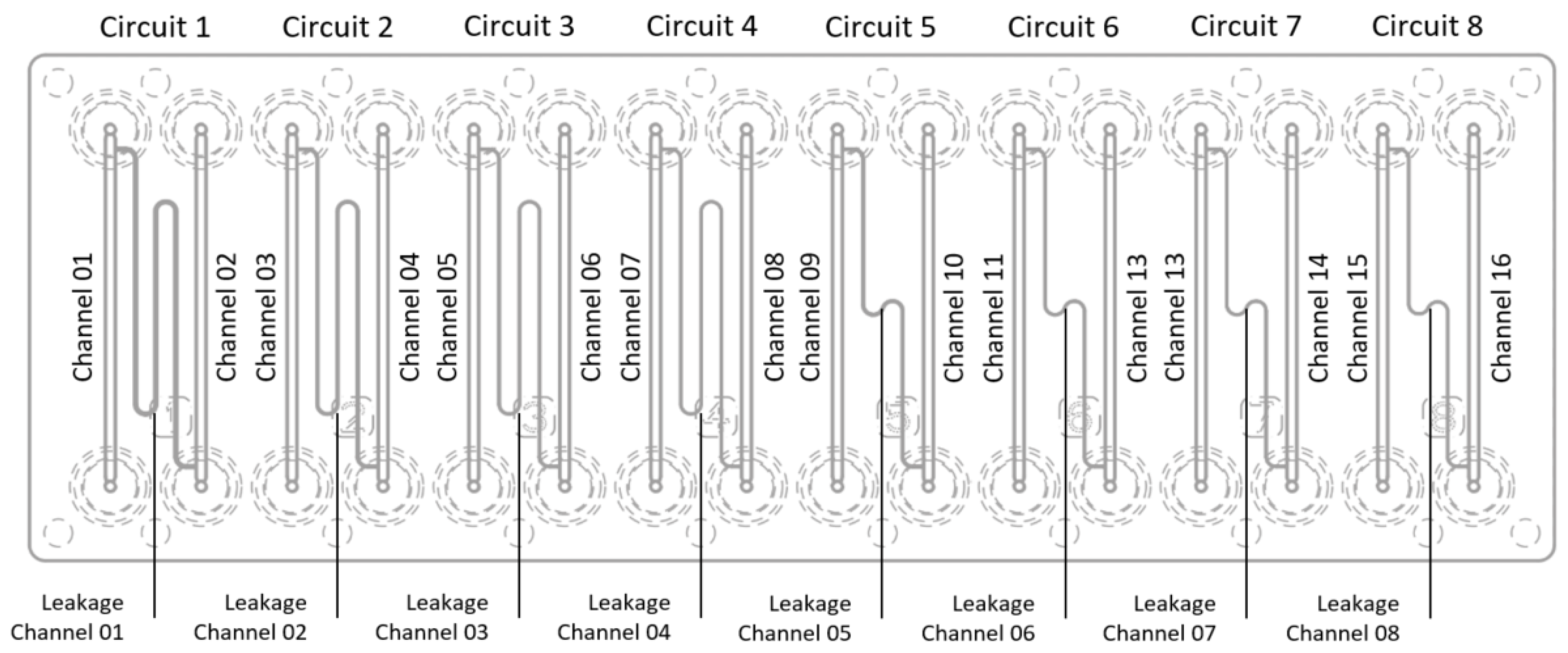
Figure 2.
Polymer chip design and its geometry nomenclature for measurements.
Figure 2.
Polymer chip design and its geometry nomenclature for measurements.
Figure 3.
Example of glass transfer standard chip, Design 04 is depicted.
Figure 3.
Example of glass transfer standard chip, Design 04 is depicted.
2.2. Polymer Transfer Standart Chips
In polymer, there was a single microscope-slide-sized chip design with eight different circuits (see
Figure 2). Each circuit consisted of two main channels with a leakage channel between them. The leakage channels are of two distinct lengths, four times the longer and four times the shorter leakage channel. The lumen of the leakage channels is rectangular and changes between circuits.
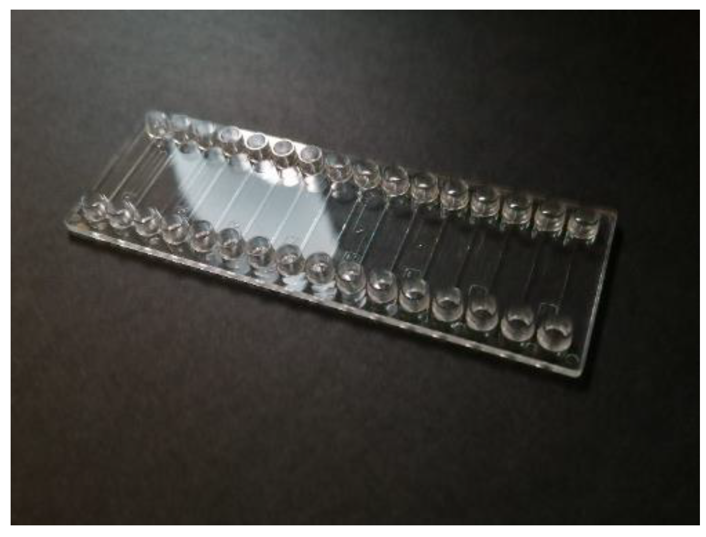
Figure 4 shows one of the polymer chips. Detailed designs, Technical drawings, and CAD files of the polymer chip design can be found in the Electronic Supplementary Information.
The polymer chips were provided by microfluidic ChipShop GmbH, Germany, who fabricated them by injection molding.
Once finished, the top part with its microfluidic structure is sealed onto a thin bottom slide to close the chip. The entire chip is made of COC (Cyclic Olefin Copolymer, tradename TOPAS©18).
3. Three Different Measurement Protocols
3.1. Protocol 1: Optical Profilometry
The first protocol entails optical profilometry. Optical profilometry is a method that uses light instead of a physical probe to characterize geometries. This allows non-destructive measurements without the need to get in direct contact with the object. Because of its light-based nature, it is particularly suitable for measurements within transparent substrates.
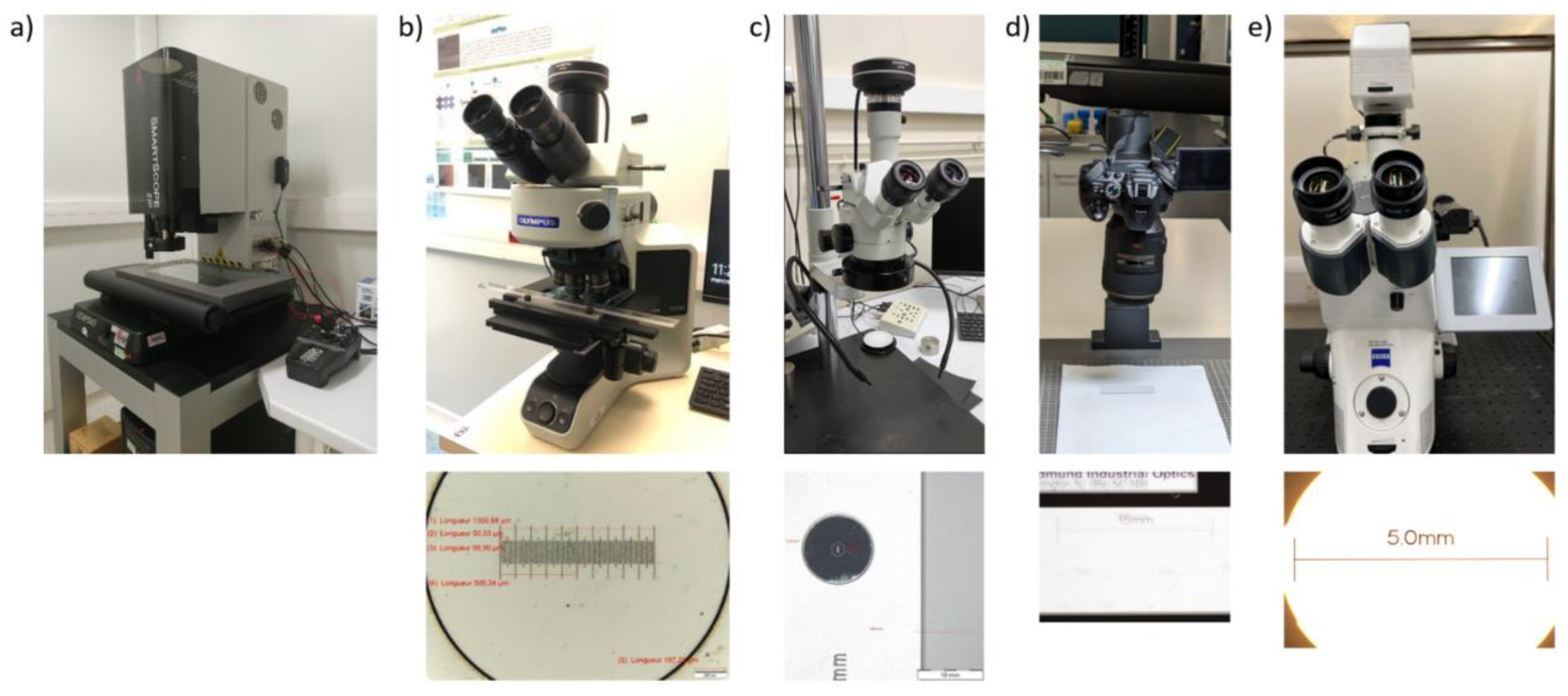
A SmartScope ZIP®250 (with its accompanying software ZONE3© (both from Optical Gaging Products (OGP) part of Quality Vision International (QVI), NY, USA) was used to perform measurements of the internal geometries.
Table 1 gives details of the instrument. The setup is shown in
Figure 5.
OGP staff annually recalibrate the instrument, which gives a guarantee for its accuracy shown in
Table 1 (Calibration report incorporated in the Electronic Supplementary Information. Please note the difference in the uncertainty between measurements where the stage has moved a distance L between two measure points and static in-image measurements.
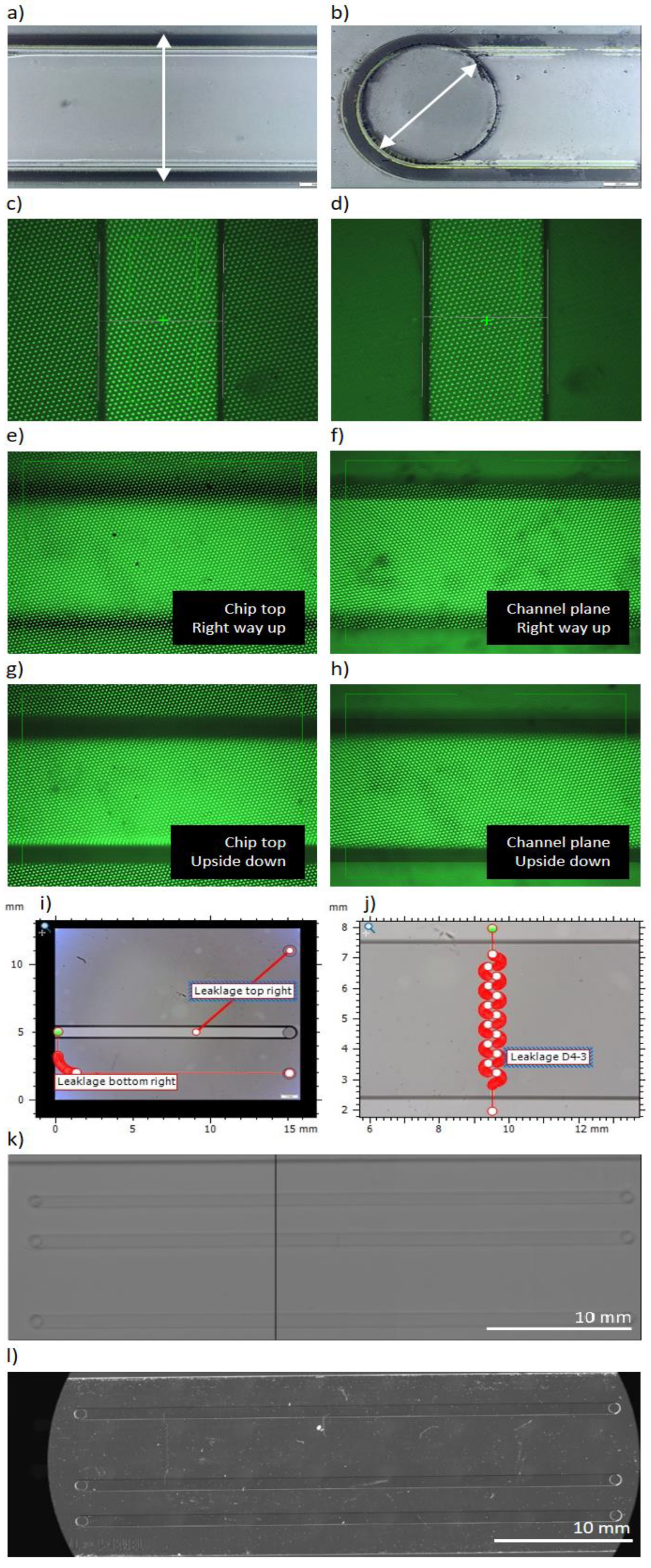
The OGP SmartScope ZIP®250 can focus automatically on a focus plane within an initially user-defined margin. The software then treats this image directly to identify geometrical features, which are then used to measure the dimension of interest. In practice this comes down to the following: To determine a channel width (main or leakage), the profilometer will find the focus plane at the top of the channel, determine the outer most edges and then measure the width between these edges (refer to
Figure 6).
The depth measurements were challenging. For the polymer chips, they were slightly more straightforward than in glass. The depths of all channels were measured by determining a focus plane at the top and at the bottom of the channel using the software’s “Focus” tool set to establish a point in 3D space on each plane. Consequently, the software measured the distance in Z between these two points to establish the channel depth (refer to
Figure 6). Depth measurements by optical profilometry inside transparent materials are subject to deformation. This deformation is a consequence of the material’s refractive index, which depends on the wavelength of the light used to find the focus plane. The SmartScope ZIP®250 uses a grid light to find its focus in Z. According to OGP, this light has a wavelength ranging from 575 to 625 nm. Thus, the polymer’s refractive index for 589 nm at 25°C,
nD=1.53, provided by microfluidic ChipShop GmbH, Germany, was used to compensate for this
To do so, all the optical profilometer’s depth measurements in the polymer chips were multiplied by
nD
For glass, the optical profilometer appeared to have issues finding different focus planes for the top and the bottom of the channels. Therefore, a more elaborate approach was adopted to estimate a channel depth. The optical profilometer was capable of establishing the top and bottom plane of the entire chip as well as one plane of a channel (refer to
Figure 6). The assumption was made, that this was the plane of the channel that was on top. In other words, when the chip was the right way up, consecutively the top of the chip, the top of the channel and the bottom of the chip could be measured. When the chip was turned over, the order inversed, and the measured channel plane changed. Therefore, when the chip is upside down, consecutively the bottom of the chip, the bottom of the channel and the top of the chip were measured. The following formula was then used to estimate the depth of the channel:
where D naturally represent the estimated channel depth, z_(chnl,2) and z_(top,2) the z-coordinates of the measurable channel plane and the top plane measured when the chip is upside down, z_(top,1)and z_(chnl,1) the z-coordinates of the measurable channel plane and the top plane measured when the chip is the right way up.
nD In this case, is the refractive index of D263©bio glass. Given the range of light provided by OGP, the glass’s refractive index for the spectral line of the center of double sodium (589.2938 nm)25
nD=1.5230, provided by Schott AG, Germany, was used to compensate for deformation17.
The length of the main channels was defined as the maximum distance between the circles of the inlet and outlet holes. The lengths of the leakage channels were established similarly. Hole diameter was determined using the “Feature finder” tool set to determine a circle on the internal hole (see
Figure 6).
For the lengths of the more complex non-linear channels, difficulty was encountered. Attempts were made with multiple different settings and ZONE3© tools to measure the lengths of the L-, U- and S-shaped channels. However, no reproducible parameters were found.
The above-described steps are programmable on the OGP SmartScope ZIP®250. This means that a specific measurement protocol including positions, fields of view, focus zones, lighting and image treatment settings can be stored in a program, allowing for repeatable tests of identical objects. Once established, a measurement program would be run three times on each chip.
Using the data from each of these runs, an average and a standard deviation (
σr) were determined. Together with the uncertainty associated with the calibration of the machine (
σc) (noted in
Table 1), a standard uncertainty of the measurement (u) is calculated using the following formula:
This is done under the assumption that these are the two largest sources of uncertainty. For the purpose of this article, the variability of the refractive index will not be taken into account. This might be work for further investigation.
3.2. Protocol 2: Optical Microscopy
The second protocol utilizes regular optical microscopy. Two different microscopes were used. Depending on the dimensional range of the microfluidic geometries of interest, either an optical microscope (Olympus BX53M) or a stereo binocular microscope (Leica Wild M3Z) was used. Details of the two instruments are included in
Table 1.
Each instrument has its own gauge structure involved in its calibration process (shown in
Figure 5). This process permits the traceability of the measurement results to the International System of Units (SI). The uncertainties associated with calibration for each instrument can be found in
Table 1.
The width and length of the leakage channels, the width of the main channels as well as the hole-diameters were all measured using the Olympus BX53M (with the x5 or x10 lens). Images were taken and analyzed using Olympus Stream Essentials 2.3.3 (Build 17023). This software includes a tool for continuously acquiring images of the object to be analyzed and automatically determining the different focal planes in a single image. It was in this final merged image that the measurements were made.
Similar as for the optical profilometer the largest dimension was taken as the width of the channel (refer to
Figure 6). For the length of the main channels, the maximum distance between the inlet and outlet holes was taken. These were measured with the Leica Wild M3Z binocular microscope. The measurements were carried out by manually adjusting the focal plane.
For the holes’ diameter, a circle tool was used. In this case, the main focal plane was difficult to identify. A large number of focal planes very close to each other can be observed. It is hypothesized that his is due to the hole-drilling step in the manufacturing process of the chips. Different measurements were performed, and an uncertainty was assessed to take into account these various focal planes and irregularities in the structure.
The length of non-linear channels (main or leakage) was measured using specific tools from the MountainsMap© version 10 software package (from Digital Surf, France). Depending on the channel shape’s complexity, either “Distance between two points” or “Customized path” were used (see
Figure 6). In both cases, the length was determined following the median line of channel width.
Measurements were run thrice on each chip and their results were treated into a standard uncertainty with the same approach as protocol 1.
3.3. Protocol 3: Tiled Digital Imagery
The third protocol uses two different instruments, both with a wide field of view. Firstly, a digital camera, a Nikon D5300 fitted with a 105 mm, 1x, f/2.8 macro lens was used. Digital cameras offer portability, affordability, and high resolution. Since they can detect events within entire microfluidic devices, they have been widely used with paper-microfluidic devices for on-site
and high-speed imaging and detection of events within microfluidic
. For the second instrument, an optical microscope similar to protocol 2 was employed. In this case, the optical microscope is a Zeiss Axio Imager equipped with a Ludl BioPoint2 motorized stage, Zeiss EC Plan Neofluar 2.5x/0.085 objective and Zeiss HRc camera. Details of both devices are included in
Table 1.
Calibration of these instruments was carried out using standard reference bars (shown in
Figure 6). This way the resolution of the instruments and the uncertainty linked to calibration can be established (included in
Table 1). The calibration report can be found in the Electronic Supplementary Information.
The measurements in this protocol were made using image treatment. For the diameters of the holes and the channel widths, both instruments could use a single image. The uncertainty of these measurements consists only of the consistency linked to calibration of the instruments.
For the length of the main channels, tiled images were used. The total number of frames for covering an entire microfluidic channel depends on the field of view of the instrument. The accuracy of the measurement is affected by how the frames are stitched together, the quality of images and uncertainty linked to calibration of the instrument.
The Nikon D5300 camera with its large field of view only needs two frames to cover an entire main channel in the glass chips (see
Figure 6 as an example). The images need to be taken with overlapped areas such that they can be stitched together in ImageJ by overlaying blemishes in successive frames. The uncertainty of overlaying is ± 3 pixels/frame (1 pixel = 8.44 m according to its calibration). However, the image quality is poor, meaning there is significant uncertainty in defining the ends of the channels. This is approximately 6 pixels at each end, so in total the error is of ± 15 pixels, which equals 0.31% of the total length of 39 800 m. Furthermore, the leakage channels were not sufficiently visible in the images to warrant reliable measurements. Together with the uncertainty linked with the instrument (0.45% see
Table 1), the potential uncertainly of the length measurements for this system is 0.76%.
The Zeiss Axio Imager contains a motorized Ludl BioPoint2 stage. Again, overlaying blemishes in adjacent image frames could achieve stitching of a composite image (see
Figure 6 as an example). In this case, however, the precision and reproducibility of the Ludl BioPoint2 stage (< 1 m) was sufficiently good such that the results were indistinguishable. The notable advantage of this instrument was the higher numerical aperture (NA) of the 2.5x objective (NA = 0.085), which gave images of better clarity, making definition of the channel and hole borders much clearer with the resulting improvement in the precision of the measurements. Therefore, the uncertainty in defining the ends is negligible (or at most at 1 pixel). Hence, the total uncertainty of the length measurements of the Zeiss Axio Imager is the same as its in-image uncertainty linked to device calibration (i.e. 0.15%, see
Table 1).
Both devices measured multiple glass chips once. For the other protocols the average of multiple measurements with a single method were taken as final measurement values. In this protocol, the average of the two measurements was taken to establish a measurement value for the protocol. Given this combination of two different methods, the standard uncertainty definition from Equation (2) needs to be updated as follows:
where
σc1 is the uncertainty associated with the Nikon D5300 (which thus differs between in-image and tiled image measurements,
Table 1),
σr2 is the uncertainty associated with calibration of the Zeiss Axio Imager and
remains the standard deviation between the two values.
3.4. Evaluation of the Measurement Results
For the evaluation of the consistency of the three protocols, their results will be tested against a reference value. For each measurement (for example the diameter of Hole 01 in Channel 01 of Design 01) a reference value can thus be defined. This reference value (called RV) is determined as the mean of the measurements values of the three protocols combined using the weighted means formula. Here, the inverse square of the standard uncertainty (
un) associated with the average of a protocol’s measurement values (
xn) serves as its weighting
:
The following formula will then give the standard uncertainty u(RV) associated with the reference
:
Once the reference value and its standard uncertainty defined, the measurement values of each protocol can be tested for consistency with this reference value. To identify this consistency the normalized error (
En) was
:
where
En serves as a protocol’s consistency indicator for a specific measurement, x_n the average of a protocol’s measurement values again, RV the reference value of the same measurement and U (
xn) and U (RV) their associated expanded uncertainties calculated as U=k*u with k=2.
With the value of En one can draw the following conclusions:
The approach described thus far allows the comparison of the protocols between each other. However, it does not necessarily say much about the accuracy of all protocols. Besides a reference value, a nominal value can be defined for all measurements as well. These nominal values and their standard uncertainties were defined by combining the dimensions in the technical design drawings with quality assurance measurements and statistical tolerances provided by IMT Masken und Teilungen AG. Thus, the nominal values aim to represent the theoretical dimensions that the geometry should have.
For the diameters of the holes no statistical data was available, so the value from the design, i.e. 800 µm was taken as nominal. Based on IMT’s experience, it was assumed that a standard uncertainty of ± 15 µm could be used, leading to an expanded uncertainty of ± 30 µm.
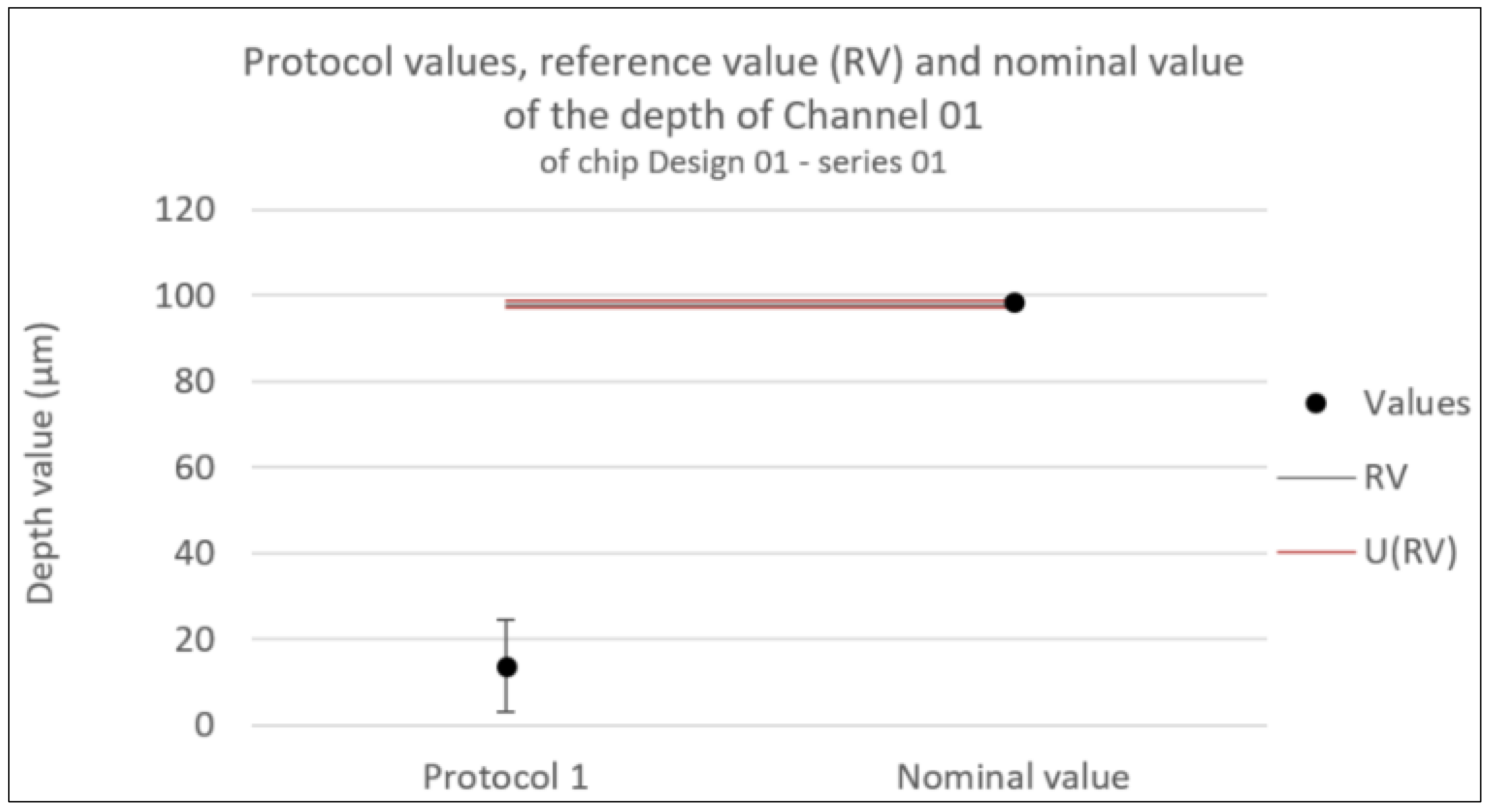
The depth was measured by IMT during quality assurance. Values were within a range of 98.3 ± 0.4µm, giving an expanded uncertainty of ± 0.8µm.
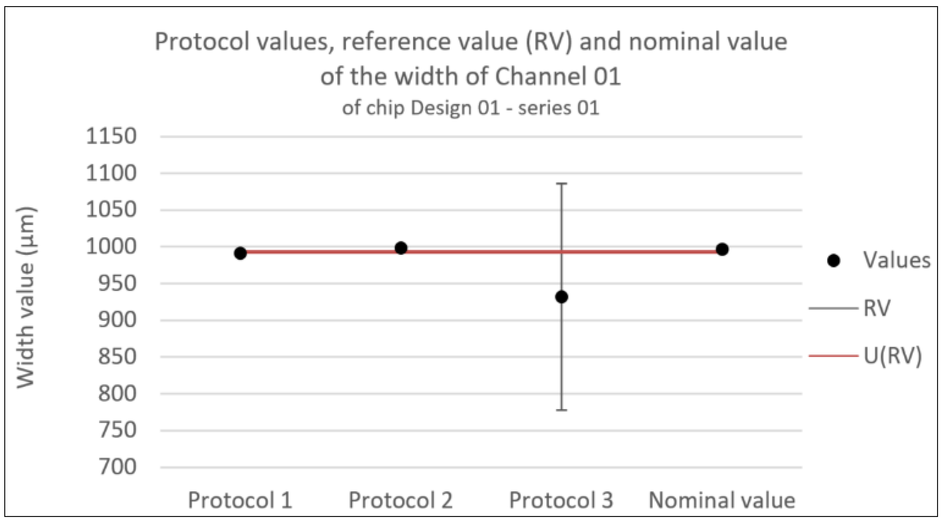
The width of the main channels was estimated knowing the depth resulting in a calculated nominal value of the width of the channels of 996.6µm ± 2.66µm for this specific batch of chips.
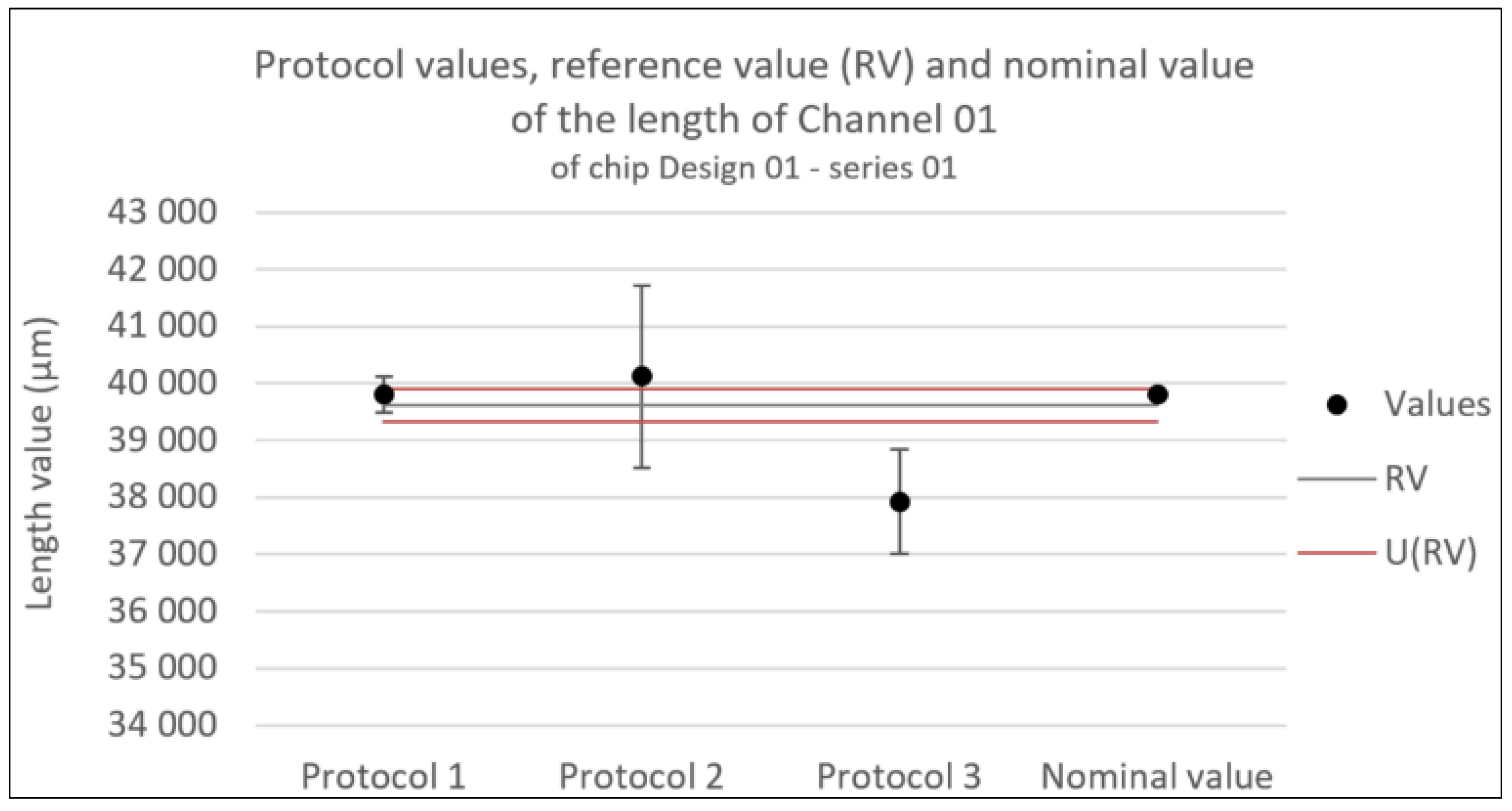
Finally, the length of the main channels, as it is measured as the maximum distance between the entrance and exit holes (designed at 39 800 µm) will depend on the precision of hole placement. Based on IMT’s experience this should have a precision of ± 7.5 µm for each hole, leading to a total standard uncertainty of ± 15 µm for the length of the main channels, thus an expanded uncertainty of ± 30 µm.
With these estimations, the consistency of the measurement values of each protocol with the nominal values can be tested.
Finally, to see the influence of material on measurements a somewhat straightforward approach was adopted. In this case, protocol 1 was applied to the glass chips as well as polymer chips. Normally the standard uncertainty of both sets of measurements would be compared. This standard uncertainty was defined in Equation (2) and consists of a standard deviation term (σr) related to the actual measurements and of an uncertainty term (σc) related to the calibration of the machine used. Since the uncertainty related to calibration of the OGP SmartScope ZIP®250 is identical for both polymer and glass measurements, it is more indicative to compare the standard deviations of the actual measurements. Thus, measurements and their standard deviations from protocol 1 on polymer and glass will be compared.
4. Results
4.1. Glass Chips
Each protocol naturally gave a set of results for the glass chips. The three complete sets of results can be found in the Electronic Supplementary Information. For analysis purposes, the results from a single chip, Design 01 – series 01, and only its first channel, Channel 01, will be treated here. In this channel, the protocols performed the following measurements:
- -
The diameter of Hole 01
- -
The diameter of Hole 02
- -
The width of the channel
- -
The depth of the channel
- -
The length of the channel
To determine the consistency between the different protocols and their resulting reference value, the normalized error values (
Ed) are shown in
Table 2.
Given that the depth was only measured with protocol 1, there is no reference value nor normalized error for a consistency test.
Finally, the consistency between the protocols and the nominal value was determined for each measurement. The normalized errors for this consistency test are shown in
Table 3.
4.2. Polymer Chips
The full set of results from the polymer chips acquired with protocol 1 can be found in the Electronic Supplementary Information. As an excerpt,
Table 4 shows the width and depth measurements as well as their standard deviations of the first circuit of one of the COC chips. To facilitate a more meaningful comparison of these standard deviations against those from measurements made on glass chips, they are expressed in percentage as well.
Thus, for comparison purposes,
Table 5 shows measurements and uncertainties of protocol 1 for the measurement directions corresponding to those of
Table 4.
5. Discusion
5.1. Comparison of Protocols
The normalized error values in
Table 2 suggest that the protocols are often inconsistent with the reference values. On the contrary,
Table 3 shows the protocols mostly consistent with the nominal values. The consistency of protocol 1 with the nominal values slightly outperforms that of protocol 2, which in turn slightly outperforms protocol 3. This implies that the different protocols all give different values, but remain consistent with the nominal values and their expanded uncertainties. Also, this reflects the need to explore the uncertainty calculation in detail since probably the are underestimated in all protocols.
Especially in the longer dimensions, the length of the channel, the accuracy of the optical profilometer is higher than the other protocols.
Several factors are hypothesized for the decreased accuracy of the length measurements of protocol 3. The most evident one being that there is an extra uncertainty term in the definition of the protocol’s standard uncertainty as a consequence of the combination of two different methods (compare Equation (2) to Equation (3)). Secondly, the uncertainty of each individual method includes an additional uncertainty associated with image stitching on top of the uncertainty associated with calibration. Thirdly, the average and standard deviations of the protocol are taken with two measurement points, one for each method. Improving any of these three factors might improve the consistency of the protocol with the nominal values for length.
In terms of uncertainty protocol 1 presents smaller values than the others in all measurement dimensions.
5.2. Close-Up on Depth Measurements
For the depth measurements visualized in
Figure 10, the only protocol capable of providing a measurement, protocol 1, is inconsistent with the nominal values (see
Table 3 and additionally
Table 5). Several factors might come into consideration to explain and possible improve this.
Firstly, the measurements are corrected with the refractive index of the material. This refractive index is given for a specific wavelength (589 nm), which is not necessarily exactly the wavelength of the SmartScope ZIP®250 used in protocol 1. OGP indicated that the wavelength of the grid light for measurements in Z could range from 575 to 625 nm. However, even if the wavelength is different from, considering the material’s change in refractive index shown in Table, it is clear that this would not significantly change the measured .
Table 6.
Refractive indices of D263©bio glass for different wavelengths spanning the SmartScope.
Table 6.
Refractive indices of D263©bio glass for different wavelengths spanning the SmartScope.
|
nC (643.8469 nm) ZIP®250 focus light range. |
1.5209 |
|
nD (589.2938 nm) |
1.5230 |
|
ne (546.074 nm) |
1.5255 ± 0.0015 |
If it is not the value refractive, then it is hypothesized that it is the way it is employed. The straightforward multiplication of measured values with the refractive index for compensation of deformation is regularly used on measurements with a single refractive interface in the structure. For an internal channel, thus having two refractive interfaces, this method was assumed to hold up. This assumption might be wrong and would merit further investigation.
A third option is that the optical profilometer does not actually measure any of the two surfaces. Given the high surface quality of wet-etched channels and the proximity of its top and bottom planes, the channel in and of itself might function as a lens. The low surface roughness, which is usually considered an advantage, might impede a proper measurement in this case. This too would be interesting for further investigation.
The hypothesis that the measurements of the optical profilometer are actually correct and the bonding process has altered the depth of the channels from an average of 98.3 ± 0.4 µm at quality assurance to the measured values of from
Table 5 seems unrealistic. This could be checked with a destructive test. Results from the other test performed on these chips within the scope of the same 20NRM02 MFMET project would have indicated such a drastic geometry change too though.
To suggest a means of further improvement of depth measurements of internal microfluidic channels an additional method was tested. The following paragraph describes preliminary results obtained during this work that could open another interesting avenue for future work on protocols of depth measurement of internal microfluidic channels.
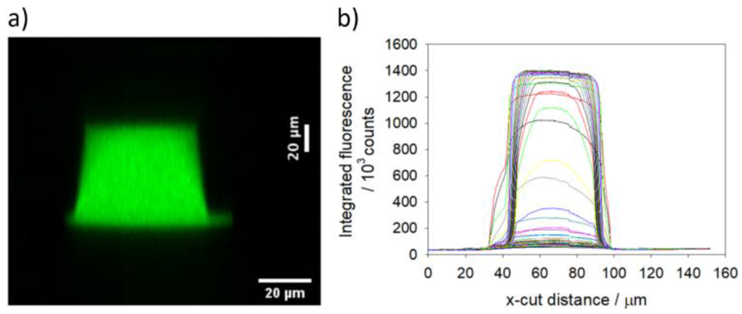
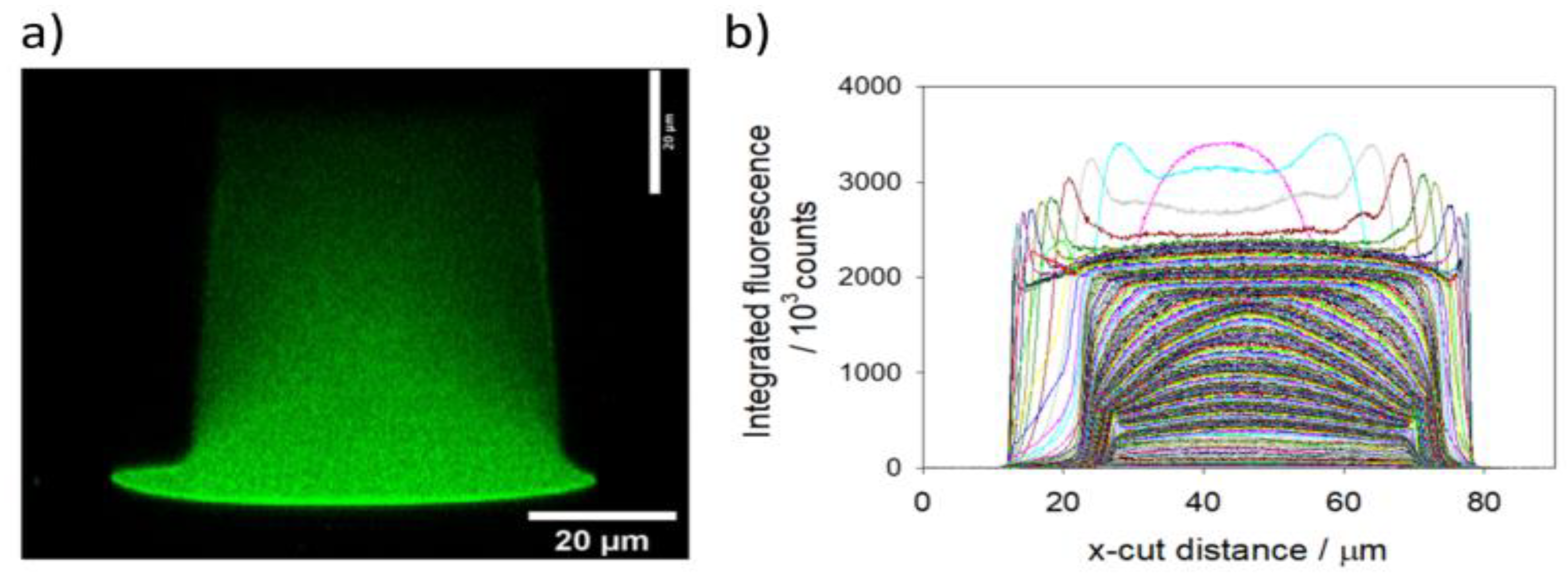
Leakage Channel 02 of a polymer chip was measured using a Zeiss LSM 510 confocal fluorescence microscope. The instrument operates based on a confocal principle, which eliminates out-of-focus light from focal planes (called optical sections) and collects serial optical sections. In comparison to conventional epifluorescence microscopy, confocal microscopy can produce three-dimensional images by stacking up a series of Z-images. Confocal microscopy is well suited to measure depth of an enclosed microfluidic channel. It must be noted that a fluorophore solution was injected into the chip for these measurements.
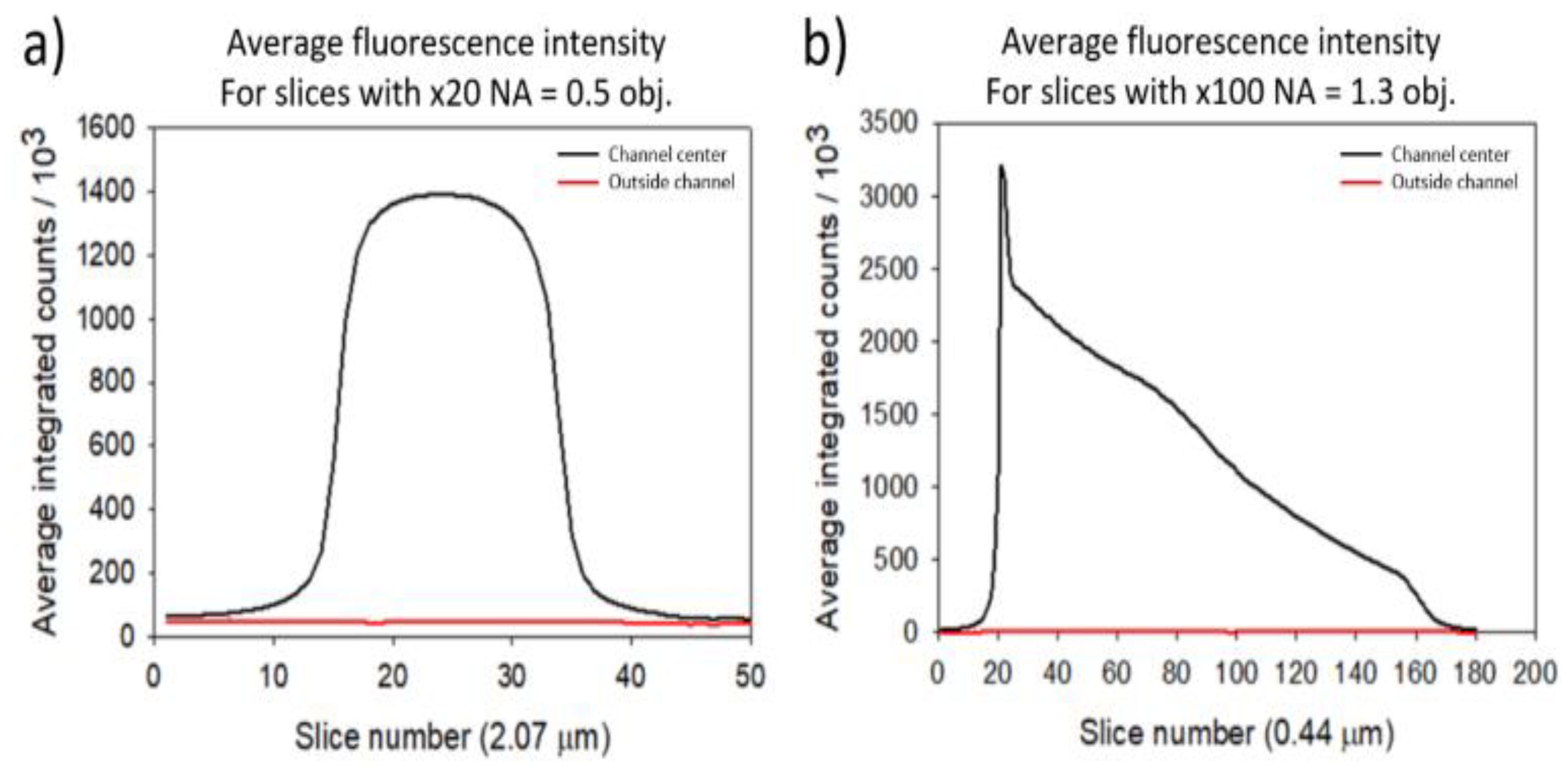
The obtainable resolution in Z depends on the NA value and the magnification of the microscope’s objectives. Two objectives were used: an x20 NA = 0.5 objective and an x100 NA = 1.3 objective. Allowing a resolution in Z of 2.07 µm and 0.44 µm respectively. The higher NA value objective thus enables thinner optical slicing. With this objective however, for optical sections further away from the base of the channel, the fluorescence intensity significantly decreases because of fluorescence self-absorption effects. This effect is clearly visible in
Figure 12.
Figure 13 and
Figure 14 show the resulting Z-stacks of the confocal fluorescence measurements made with the x20 N=0.5 objective and the x100 NA = 1.3 objective respectively.
To estimate the channel height using these confocal measurements, first it is necessary to determine the sections at which the fluorescence intensity in the channel is significant compared to outside the channel. This can be done by comparing the intensity at the center of the channel to the intensity measured outside of the channel (such as shown in
Figure 12).
Secondly, a decision needs to be made about the minimum value of fluorescence intensity within an optical section corresponds to that confocal slice being substantially within the channel. This decision is necessary because the confocality is not perfect i.e. for all practical pinhole sizes light from a range of Z-distances will pass through. For a homogeneous fluorescence solution, such as the one in use here, a lower limit for fluorescence intensity to determine whether an optical section is substantially within the channel could for example be taken as 1% of that found at the channel’s mid-height.
Using this 1% criteria, it is possible to estimate that 37 of the 50 optical sections from the x20 NA = 0.5 objective are substantially within the channel. With its resolution in Z of 2.07 µm (calibrated to be accurate to 0.1 µm using an internal encoder), the channel height of the polymer device is estimated at 74.5 ± 4 µm (there will be at least on slice uncertainty at both the top and bottom of the channel).
Despite the fact that the profiles collected using the x100 NA = 1.3 objective appear noisy (especially at sections further from the channel base), it is possible to make an accurate estimate of which slices have a fluorescence intensity above the 1% threshold. For the x100 NA = 1.3 objective there are 166 out of 180 optical sections above the 1% fluorescence intensity criteria, corresponding to a channel height estimate of 73.0 ± 0.8 µm.
Thus, the two measurements are consistent with each other with the x100 NA = 1.3 objective having greater precision.
There is a channel height discrepancy between the design specifications and the height measured by confocal microscopy. These parts are made by sealing an upper piece, which bears the imprinted channel profile, to a lower piece that is a plain (flat) plastic substrate. A significant fraction of this discrepancy in heights is most likely due to the bonding process used to seal the two pieces together. As can be seen from the fluorescence x-cut profiles of
Figure 13 and
Figure 14, the measured width of the lowest 5 – 10 µm of the channel is significantly larger than the main part of the channel (at approximately 30 µm above the base). If this lower, wider part of the channel profile is disregarded, and the fluorescence criteria used to define the channel height is relaxed from 1% to 5% of the main channel intensity, then the measurement of upper piece channel height becomes 56 µm, significantly closer to the design specification of 50 µm.
These preliminary results hint in the direction of another interesting method worth investigating in future work for depth measurements of internal channels in transparent microfluidic devices.
5.3. The Influence of Different Materials
Following the comparison between protocols, the influence of different materials on measurements will be regarded. Measurements done on polymer and on glass chips in XY-plane will be considered separately from the measurements in Z.
The standard deviations in the XY-plane (the width in
Table 4 and
Table 5) generally in the order of a few tenths of micrometers for both polymer and glass measurements. When considering the percentages, it becomes even more evident that the standard deviation of measurements is negligible for both materials.
It might be interesting for future research to see if this observation holds up for other materials common in microfluidics (e.g. PP, PC, COP, PMMA) and measurement methods (e.g. optical or confocal microscopy) as well. Experience would suggest that this apparent indifference to the material of the SmartScope ZIP®250 is not necessarily shared by other techniques.
In contrast, the standard deviations of the depth measurements in TOPAS© COC appear much better than those in D263©bio glass.
While measuring, it was noticed that the SmartScope ZIP®250 appeared to be able to better distinguish the top and bottom plane of the internal channel in the polymer chips. This is why in the protocol the Z-coordinates of the top and the bottom are simply subtracted to calculate the channel depth. To come back to the point made earlier on surface roughness, it is hypothesized that, in this specific case, the higher roughness of the polymer chips that is usually a disadvantage, might allow the optical profilometer to better define a focus plane than on the near perfectly smooth wet-etched glass channels. Testing this hypothesis could be interesting future work.
It is worth noting that, regardless a low or high standard deviation, the depth measurement’s accuracy in both materials is questionable. In both TOPAS© COC and D263©bio glass the depth measurements are inconsistent with their nominal values. In addition, even though apparently capable of distinguishing the bottom from the top of the internal channel in the polymer chips, it is difficult to distinguish it from the actual bottom of the chip. This might for example play a role in the overestimation of the depth of Leakage Channel 01 shown in
Table 4.
5. Conclusions
Given the commonly acknowledged challenge of accurately measuring internal structures after chip assembly within the microfluidic industry, this work, performed as part of the MFMET project, has compared three different protocols: optical profilometry, optical microscopy and tiled digital imagery for the measurement of different internal microfluidic structures in chips made of D263©bio glass and TOPAS© COC.
A consistency analysis by normalized error statistics revealed protocol 1, optical profilometry, as the preferred method due to its low uncertainty compared to the other protocols and its higher consistency with nominal geometry values.
For the measurement of the depth of internal geometry, difficulty was encountered. The only protocol able to provide a measurement of the internal channel depth, optical profilometry, gave results that are highly inconsistent with their nominal values. Different avenues of future work are proposed including a study of how to apply the refractive index for deformation compensation when challenged with multiple refraction interfaces. Another possible method that was shown to merit further investigation is confocal fluorescence microscopy, which showed promising preliminary results.
TOPAS© COC chips did not give significantly worse or better results than the D263©bio chips. Based on which the conclusion can be drawn that the materials are equivalently compatible with optical profilometry. Here too, the depth measurements form an exception. Paradoxically the channels with worse surface roughness were better measurable with the optical profilometer. Despite that, depth measurements in the TOPAS© COC chips were not satisfactory either. Further research comparing other common materials in microfluidics and measurement techniques is recommended.
The results of this work directly address the current lack of measurement methods for internal microfluidic structures by providing a comprehensive comparison of different protocols, ultimately suggesting a preferred option for immediate application within the microfluidic industry. Additionally, this study offers valuable directions for future research, serving as an initial step in overcoming a significant challenge that impedes the microfluidic industry from realizing its revolutionary potential.
Author Contributions
EB and KR were responsible for the conceptualization and supervision of the study. JK performed investigations of protocol 1, defining its methodology and providing the required resources. NF did the same for protocol 2 with assistance in the investigations from ML as did HY for protocol 3 and the confocal microscopy assisted in the investigations by AG. Formal analysis of all results was performed by EB and JK. The original draft was written by JK starting from input by EB, HY and NF for their respective parts. All authors contributed to the review and editing of the manuscript.
Funding
This project 20NRM02 MFMET has received funding from the EMPIR programme co-financed by the Participating States and from the European Union’s Horizon 2020 research and innovation programme.
Acknowledgments
The authors would like to express their gratitude to IMT Masken und Teilungen AG, Switzerland, and microfluidic Chipshop GmbH, Germany, for their contribution to the project, including but not limited to the development of the transfer standard chips used in this work. Besides, the authors want to thank all academic and industrial partners for continuously providing insights in microfluidic challenges and needs through discussions, workshops, or surveys conducted by The Microfluidics Association.
Conflicts of interest: There are no conflicts to declare.
References
- Whitesides, G.M. , Nature, 2006, 442, 368–373.
- Sackmann, E.K.; Fulton, A.L.; Beebe, D.J. , Nature, 2014, 507, 181–189.
- deMello, A.; Elvira, K.S. , Nat Chem, 2013, 5, 905–915.
- Berlanda, S.F.; Breitfeld, M.; Dietsche, C.L.; Dittrich, P.S. , Anal Chem, 2021, 93, 311–331.
- Convery, N.; Gadegaard, N. , Micro and Nano Engineering, 2019, 2, 76–91.
- Rosen Y, G.P. , Curr Pharm Biotechnol, 2010, 11, 366–375.
- Behera, P.P.; Kumar, N.; Kumari, M.; Kumar, S.; Mondal, P.K.; Arun, R.K. , Sensors & Diagnostics, 2023, 2, 1437–1459.
- Huh, D.; Leslie, D.C.; Matthews, B.D.; Fraser, J.P.; Jurek, S.; Hamilton, G.A.; Thorneloe, K.S.; McAlexander, M.A.; Ingber, D.E. , Science Translational Medecine.
- Levner, D.; Ewart, L. , Expert Opin Drug Discov, 2023, 18, 1313–1320.
- Quintard, C.; Tubbs, E.; Jonsson, G. , Nat Commun.
- Middelkamp, H.; Weener, H.; Gensheimer, T.; van der Meer, A.D. , Biomedical Devices.
- Yole Intelligence, Status of the Microfluidics Industry 2023, 2023.
- Wang, K.; Man, K.; Liu, J.; Chen, Q.; Zhou, Y.; Yang, Y. , ACS Biomater Sci Eng, 2020, 6, 3231–3257.
- Kim, H.; Lee, J.B.; Kim, K.; Sung, G.Y. , Journal of Industrial and Engineering Chemistry, 2022, 115, 279–286.
- Gurkan, U.A.; Wood, D.K.; Carranza, D.; Herbertson, L.H.; Diamond, S.L.; Du, E.; Guha, S.; Di Paola, J.; Hines, P.C.; Papautsky, I.; Shevkoplyas, S.S.; Sniadecki, N.J.; Pamula, V.K.; Sundd, P.; Rizwan, A.; Qasba, P.; Lam, W.A. , Lab Chip, 2024, 24, 1867–1874.
- van Heeren, H. , Trends and Challenges in the Microfluidic Industry, 2021.
- Schott, A.G., D263©, https://www.schott.com/en-nl/products/d-263-P1000318/technical-details?tab=830fa6759ac84d07a3d53bfbe4535a90, (accessed 17 April 2024).
- TOPAS Advanced Polymers/Polyplastics, TOPAS© COC Datasheets.
- Batista, E.; Reyes, D.R. , Publishable Summary Establishing metrology standards in microfluidic devices (20NRM02), 2023.
- MFMET, MFMET – Establishing Metrology Standards in Microfluidic Devices, https://mfmet.eu/, (accessed 18 April 2024).
- Silverio, V.; Guha, S.; Keiser, A.; Natu, R.; Reyes, D.R.; van Heeren, H.; Verplanck, N.; Herbertson, L.H. , Front Bioeng Biotechnol, 2022, 10.
- Copeland, M.; Ogheard, F.; Batista, E.; van Heeren, H. , Flow resistivity testing, 2023.
- ISO/TC 48, ISO 22916:2022 Microfluidic devices Interoperability requirements for dimensions, connections and initial device classification, 2022.
- microfluidic ChipShop GmbH, Material Data Sheet mcs-COC 13, 2024.
- Schott, A.G. , TIE-29 Refractive Index and Dispersion, 2016.
- Martinez, A.W.; Phillips, S.T.; Carrilho, E.; Thomas, S.W.; Sindi, H.; Whitesides, G.M. , Anal Chem, 2008, 80, 3669–3707.
- Wang, B.; Li, Y.; Zhou, M. , Nat Commun, 2023, 14, 1341.
- Howell, J.; Hammarton, T.C.; Altmann, Y.; Jimenez, M. , Lab Chip.
- Cox, M.G. , Metrologia, 2002, 39, 589–595.
- ISO/TC 69/SC 6, ISO 13528:2022 Statistical methods for use in proficiency testing by interlaboratory comparison, 2022.
Figure 4.
Example of a polymer transfer standard chip.
Figure 4.
Example of a polymer transfer standard chip.
Figure 5.
Different setups for dimension measurements. a) Optical profilometer OGP SmartScope ZIP®250. b) Optical microscope Olympus BX53M with its calibration gauge. c) Stereo binocular microscope Leica Wild M3Z with its calibration gauge. d) Digital camera Nikon D5300 with its calibration gauge. e) Optical microscope Zeiss Axio Imager with its calibration gauge.
Figure 6.
Definition of measurements. a) The width of the channels is taken as the maximum width. b) The diameter of the holes is taken as a feature recognition of the internal hole. c) Point on the bottom Z-plane of the polymer channel. d) Point at the top Z-plane of the polymer channel. e) Point on the top plane of the glass chip when the chip is the right way up. f) Point on the measurable channel plane of the glass chip when the chip is the right way up. g) Point on the top plane of the glass chip when the chip is upside down. h) Point on the measurable channel plane of the glass chip when the chip is upside down. i) MountainsMap©’s “Distance between two points” and “Customized path” tools applied to design 08. j) MountainsMap©’s “Distance between two points” and “Customized path” tools applied to S-channel in design 04. k) A stitched image for Design 01 using the Nikon D5300 camera. l) A stitched image for Design 04 using the Zeiss Axio Imager with Ludl BioPoint2 stage.
Figure 7.
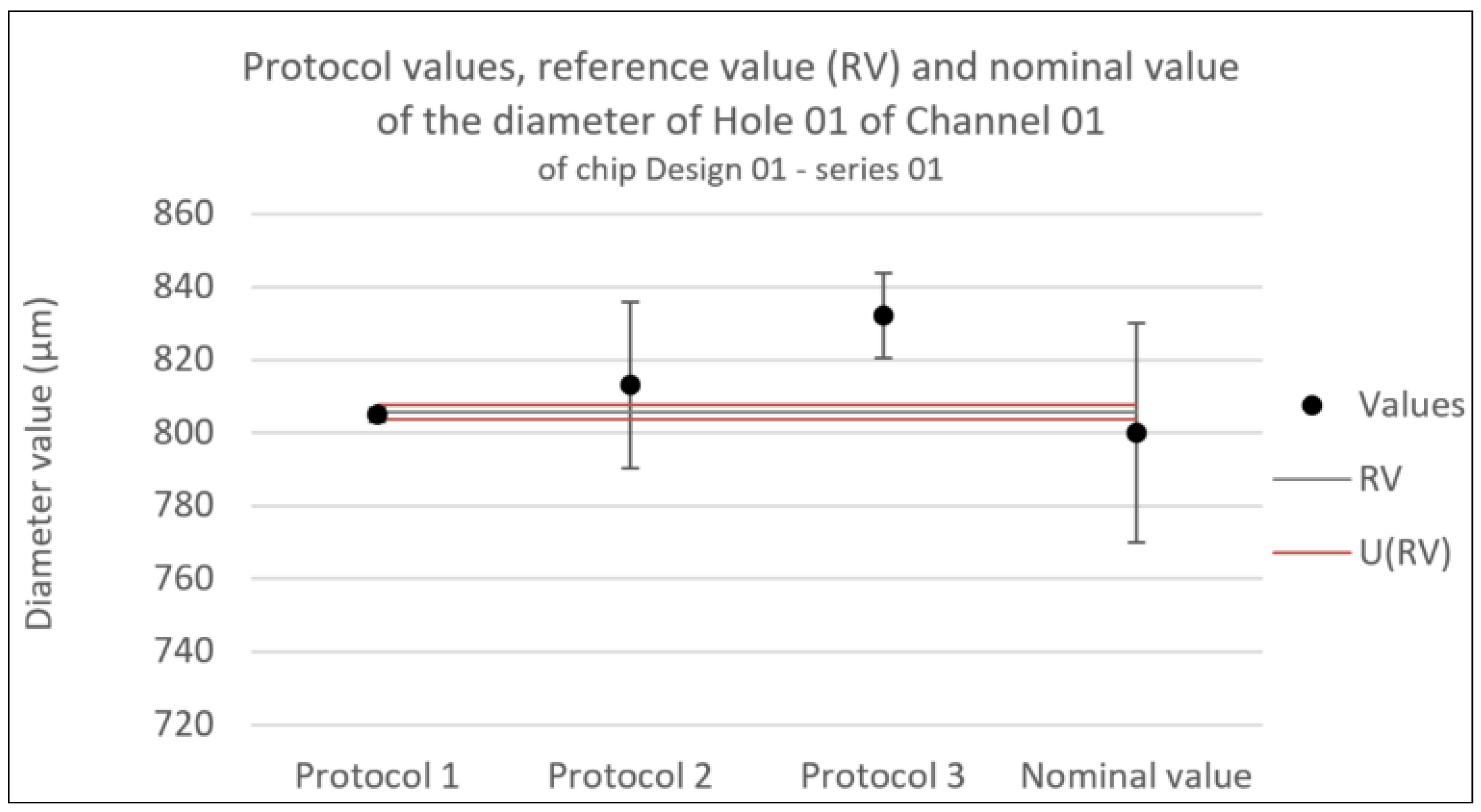
Consistency test for the diameter of Hole 01 in Channel 01 of chip Design 01 - series 01. Error bars represent the expanded uncertainty. Likewise U(RV) is the expanded uncertainty associated with the reference value.
Figure 7.
Consistency test for the diameter of Hole 01 in Channel 01 of chip Design 01 - series 01. Error bars represent the expanded uncertainty. Likewise U(RV) is the expanded uncertainty associated with the reference value.
Figure 8.
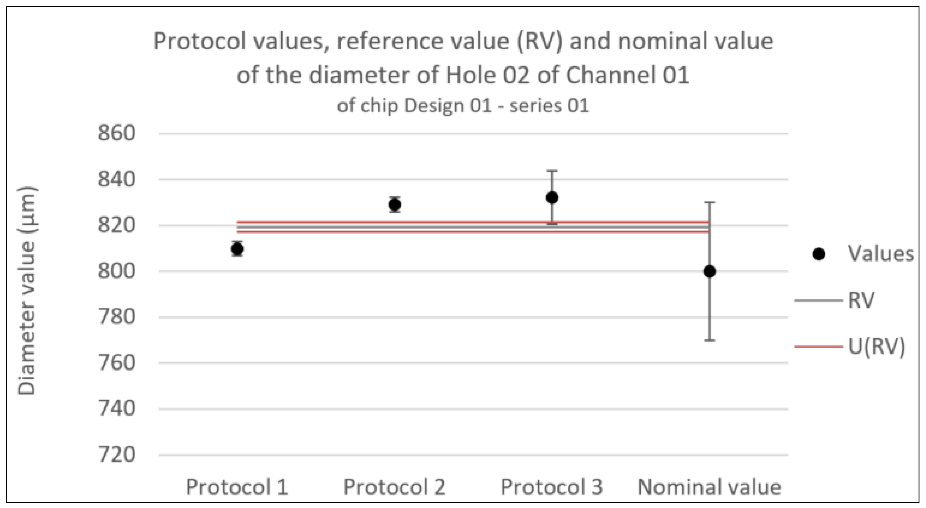
Consistency test for the diameter of Hole 01 in Channel 01 of chip Design 01 - series 01. Error bars represent the expanded uncertainty. Likewise U(RV) is the expanded uncertainty associated with the reference value.
Figure 8.
Consistency test for the diameter of Hole 01 in Channel 01 of chip Design 01 - series 01. Error bars represent the expanded uncertainty. Likewise U(RV) is the expanded uncertainty associated with the reference value.
Figure 9.
Consistency test for the width of Channel 01 of chip Design 01 - series 01. Error bars represent the expanded uncertainty. Likewise U(RV) is the expanded uncertainty associated with the reference value.
Figure 9.
Consistency test for the width of Channel 01 of chip Design 01 - series 01. Error bars represent the expanded uncertainty. Likewise U(RV) is the expanded uncertainty associated with the reference value.
Figure 10.
Consistency test for the depth of Channel 01 of chip Design 01 - series 01. Error bars represent the expanded uncertainty. Likewise U(RV) is the expanded uncertainty associated with the reference value.
Figure 10.
Consistency test for the depth of Channel 01 of chip Design 01 - series 01. Error bars represent the expanded uncertainty. Likewise U(RV) is the expanded uncertainty associated with the reference value.
Figure 11.
Consistency test for the length of Channel 01 of chip Design 01 - series 01. Error bars represent the expanded uncertainty. Likewise U(RV) is the expanded uncertainty associated with the reference value.
Figure 11.
Consistency test for the length of Channel 01 of chip Design 01 - series 01. Error bars represent the expanded uncertainty. Likewise U(RV) is the expanded uncertainty associated with the reference value.
Figure 12.
Average fluorescence intensity for successive optical sections (slices) measured in the center of the channel (black) and to the side of the channel (red). Base of the channel at slice 0. a) Measurements from the x20 NA = 0.5 objective, 2.07 µm sections. b) Measurements from the x100 NA = 1.3 objective, 0.44 µm sections.
Figure 13.
Integrated fluorescence intensity from Z-stack of all 50 optical sections taken with the x20 NA = 0.5 objective. a) cross-section of channel height. b) Fluorescence Intensity profile of all optical sections over an x-cut perpendicular to both the long channel axis and the channel height axis.
Figure 14.
Integrated fluorescence intensity from Z-stack of all 180 optical sections taken with the x100 NA = 1.3 objective. a) cross-section of channel height. b) Fluorescence Intensity profile of all optical sections over an x-cut perpendicular to both the long channel axis and the channel height axis.
Table 1.
Specifications of the different instruments used for dimension measurements.
Table 1.
Specifications of the different instruments used for dimension measurements.
| Instrument |
Range |
Lens |
Lighting |
Calibration |
Uncertainty linked to calibration |
| OGP SmartScope ZIP®250 |
> 1 µm |
x 1
x 2 |
Substage LED profile
Coaxial LED surface
SmartRing™ LED ring light |
Annual calibration report by OGP |
In plane (XY):
± 2 µm + 4L/1000
Vertically (Z):
± 2.5 µm + 5L/1000
In-image:
< 1 µm |
| Olympus BX53M |
< 10 000 µm |
x 1.5
x 5
x 15 |
|
Test pattern (see Figure 5) |
0.1 % |
| Leica Wild M3Z |
> 10 000 µm |
x 2.56 |
|
Test pattern (see Figure 5) |
2 % |
| Nikon D5300 |
> 10 000 µm |
x 1, f/2.8,
105 mm macro lens |
|
Test pattern (see Figure 5) |
In-image:
0.45 %
On tiled images:
0.76 % |
| Zeiss Axio Imager |
< 10 000 µm |
x 2.5 |
|
Test pattern (see Figure 5) |
0.15 % |
Table 2.
Normalized error values between protocols and their resulting reference value RV for each measurement. Normalized error values indicating inconsistency are marked in red.
Table 2.
Normalized error values between protocols and their resulting reference value RV for each measurement. Normalized error values indicating inconsistency are marked in red.
| |
Diameter
Hole 01 |
Diameter Hole 02 |
Width |
Depth |
Length |
| Protocol 1 |
-1.78 |
-4.44 |
-1.57 |
N/A |
1.48 |
| Protocol 2 |
0.33 |
4.14 |
1.65 |
N/A |
0.32 |
| Protocol 3 |
2.30 |
1.12 |
-0.40 |
N/A |
-1.95 |
Table 3.
Normalized error values between protocols and the nominal value for each measurement. Normalized error values indicating inconsistency are marked in red.
Table 3.
Normalized error values between protocols and the nominal value for each measurement. Normalized error values indicating inconsistency are marked in red.
| |
Diameter
Hole 01
|
Diameter Hole 02 |
Width |
Depth |
Length |
| Protocol 1 |
0.16 |
0.33 |
-0.93 |
-7.81 |
0.02 |
| Protocol 2 |
0.35 |
0.96 |
0.23 |
N/A |
0.20 |
| Protocol 3 |
0.99 |
0.99 |
-0.42 |
N/A |
-2.04 |
Table 4.
Measurements of the width and depth of the channels in circuit 1 of one of the TOPAS(C) COC chips as well as their associated standard deviations.
Table 4.
Measurements of the width and depth of the channels in circuit 1 of one of the TOPAS(C) COC chips as well as their associated standard deviations.
| |
Width |
Depth |
| |
Average measured |
Standard deviation |
Average measured |
Standard deviation |
| Channel 01 |
503.1 µm |
0.1 µm
(0.0 %) |
358.0 µm |
1.7 µm (0.5 %) |
| Leakage Channel 01 |
108.5 µm |
0.1 µm
(0.1 %) |
123.6 µm |
1.8 µm (1.4 %) |
| Channel 02 |
508.1 µm |
0.1 µm
(0.0 %) |
372.9 µm |
2.7 µm (0.7 %)
|
Table 5.
Measurements of the width and depth of the channels of glass chip Design 01 - series 01 as well as their associated standard deviations.
Table 5.
Measurements of the width and depth of the channels of glass chip Design 01 - series 01 as well as their associated standard deviations.
| |
Width |
Depth |
| |
Average measured |
Standard deviation |
Average measured |
Standard deviation |
| Channel 01 |
991.3 µm |
0.2 µm
(0.0 %) |
13.8 µm |
4.6 µm
(33.0 %) |
| Channel 02 |
992.1 µm |
0.2 µm
(0.0 %) |
17.9 µm |
1.3 µm
(7.6 %) |
| Channel 03 |
992.4 µm |
0.2 µm
(0.0 %) |
20.2 µm |
3.3 µm
(16.3 %) |
| Leakage Channel |
143.0 µm |
0.5 µm
(0.3 %) |
N/A |
N/A |
|
Disclaimer/Publisher’s Note: The statements, opinions and data contained in all publications are solely those of the individual author(s) and contributor(s) and not of MDPI and/or the editor(s). MDPI and/or the editor(s) disclaim responsibility for any injury to people or property resulting from any ideas, methods, instructions or products referred to in the content. |
© 2024 by the authors. Licensee MDPI, Basel, Switzerland. This article is an open access article distributed under the terms and conditions of the Creative Commons Attribution (CC BY) license (http://creativecommons.org/licenses/by/4.0/).
