1. Introduction
Dielectric elastomer actuators (DEAs) have recently received considerable attention from researchers, which has a simple structure but with high energy density [
1], low power consumption (on the order of mW) [
2], and high deformation capacity(≥100%). DEAs have demonstrated their potential in various applications due to these advantageous characteristics. One significant application is the field of soft robotics [
3,
4,
5], where their high deformation capability enables the creation of robots capable of intricate movements mimicking biological organisms, such as driving wings of tiny flying robots [
6,
7], fins of fish robots [
8], and mimicking natural muscles [
9,
10]. Moreover, DEAs find utility in tunable optics [
11,
12,
13] and sensors [
14], broadening their potential applications.
DEAs usually comprise two flexible electrodes, mainly composed of carbon powder and graphite [
15], with a flexible film sandwiched between them shown in
Figure 1. When voltage is applied to the electrodes, opposite charges accumulate on each electrode, inducing Maxwell stress in the thickness direction. This stress compresses the flexible film between the electrodes, causing the incompressible film to expand in all directions, as depicted in
Figure 2. Such expansion can lead to a large strain exceeding 100%. Maxwell stress follows the following formula:
where
P represents Maxwell stress, ε
0 denotes the dielectric constant of vacuum, ε
r signifies the dielectric coefficient of the elastomer,
V is the voltage, and
d indicates the thickness of the elastomer. According to Eq. (1), the deformation induced by the elastomeric material is directly proportional to the square of the applied voltage, typically around 100 V/μm. Considering that the thickness of the dielectric elastomer film is generally in the range of tens of micrometers, achieving a sufficiently significant deformation requires applying voltage at the kilovolt level, despite the low power requirement. Generating high voltages above the kilovolt level generally requires a relatively large circuit. However, such a setup is challenging for certain applications of DEAs, such as tiny flying robots, making the miniaturization of the DEA drive circuits essential. Furthermore, DEAs are often required to generate complex, controllable waveforms under specific conditions, such as precisely actuating artificial muscles or synchronizing the movement of multiple wings on flying robots. This necessitates a high-voltage power supply capable of delivering arbitrary waveforms and an integrated circuit design that supports multiple channels without crosstalk. Meeting these demands introduces a challenge to the development of the DEA driving circuits.
Unfortunately, there is currently no available commercial product that meets all the necessary features. High-voltage power supplies commonly used in laboratories are bulky, heavy, and not portable. Researchers have made numerous efforts to address this challenge and develop appropriate high-voltage power supplies. Reference [
16] utilized commercial high-voltage converters to create open-source portable high-voltage power supplies, offering cost-effectiveness and capability of delivering high voltages exceeding the kilovolt level. In scenarios that require multi-channel drives, connecting multiple drive boards in series will occupy more volume and complicate the structure. Reference [
17,
18] discusses three designs of miniaturized high-voltage drive circuits, employing integrated high-voltage converters or custom high-voltage amplification structures respectively. These designs can output four channels of variable high-voltage square wave drive signals. However, the independence of these channels is limited because they share the same high voltages. Consequently, if different types of dielectric elastomer films with distinct breakdown voltages or thicknesses are utilized in the device, it may lead to breakdown issues. Reference [
19] developed a low-cost high-voltage converter utilizing the Cockcroft-Walton circuit. However, it occupies a significant amount of space. Some researchers have proposed models aimed at converting low voltage into high voltage [
20,
21,
22,
23,
24,
25], but they have not addressed the challenge of multichannel driving.
To meet the diverse characteristics required by DEAs driving circuits, this paper introduces a four-channel high-voltage power supply for DEAs. Each channel is capable of independently generating high voltages ranging from 100 to 6000 V. With programmable control, the system can generate a wide array of waveform shapes. Each channel operates autonomously without mutual interference. The high-voltage discharge rate imposes certain constraints on the waveform generation. Specifically, the voltage difference between adjacent sampling points must adhere to a particular relationship to maintain the integrity of the waveform:
where Δ
V denotes the voltage difference between successive sampling points,
VSR signifies the slew rate of the circuit (discharge rate),
N is the total number of sampling points per cycle, and
f corresponds to the waveform frequency. Tests have demonstrated that at the 200th sampling point, the system can generate any waveform within the output voltage range at frequencies ranging from 0.1 Hz to 0.5 Hz. The compact design of the entire circuit measures approximately 80 × 80 × 50 mm
3, ensuring portability and ease of integration. Moreover, it includes an intuitive user interface for generating common waveforms, enhancing accessibility and usability.
2. Materials and Methods
This proposed power supply involves two separate printed circuit board (PCB) components, responsible for signal generation and high-voltage amplification functions independently. The primary function of the signal generation part is to produce adjustable low-voltage signals, while the high-voltage amplification part amplifies and processes these signals. The advantages of this design include (1) Safety and isolation: By physically segregating high-voltage and low-voltage signals, this design effectively mitigates potential maloperations during use, safeguarding low-voltage circuits against potential high-voltage damage. This isolation strategy not only enhances system security but also bolsters the stability and reliability of each component. (2) Flexibility and scalability: The autonomy of the high-voltage amplification section provides significant flexibility for the system’s application scenarios. Depending on specific requirements, the signal generation part can be replaced to integrate a low-voltage signal source that is better suited to particular application needs. This modular design approach greatly expands the system’s versatility and facilitates future technological upgrades and functional expansions. These two parts are connected with wiring terminals.
2.1. Signal Generation
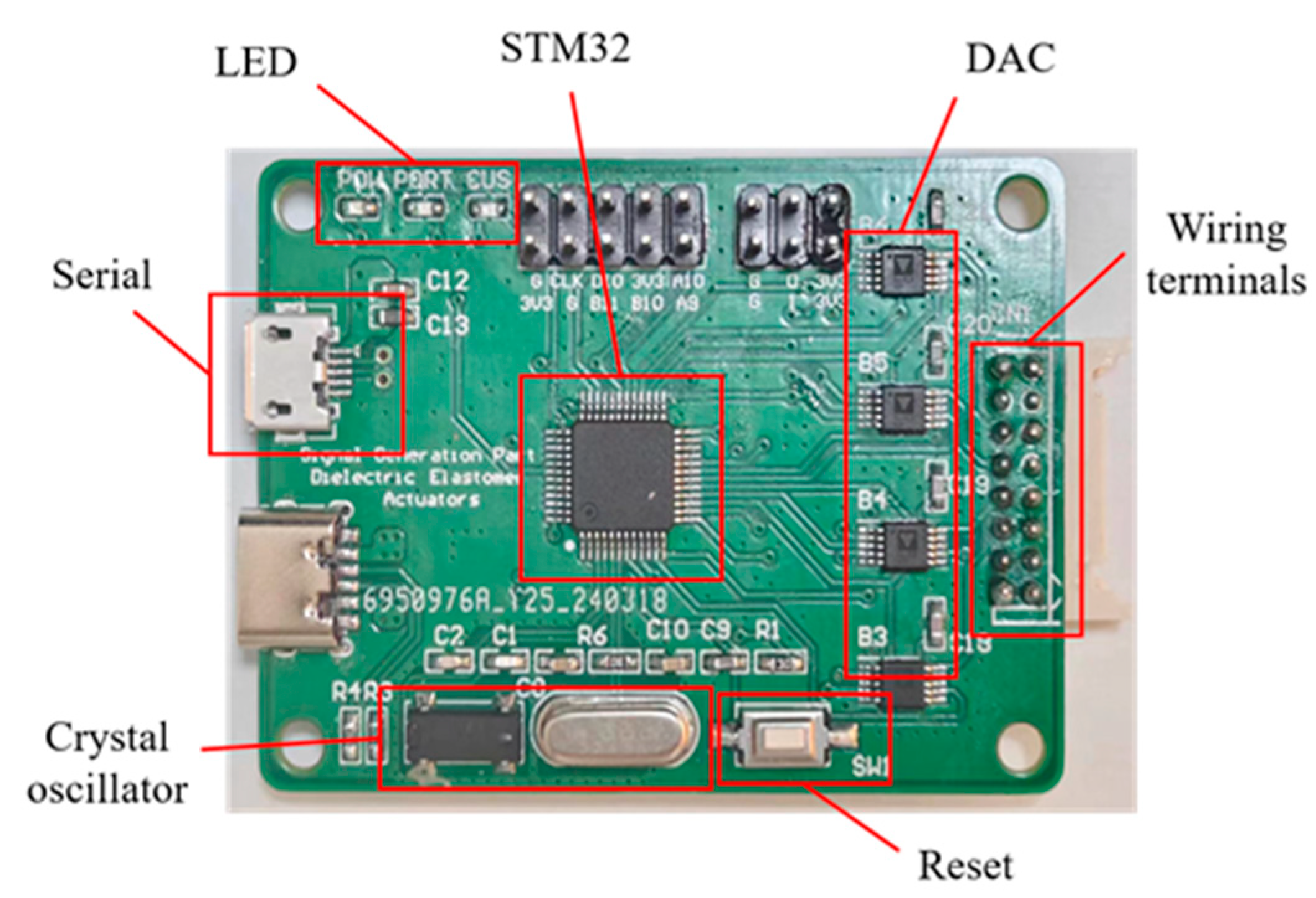
The signal generation component in this paper is realized using a printed circuit board (PCB), as depicted in
Figure 3, which can receive control signals from a personal computer through a serial communication interface (UART). The signal generation process involves integrating a complete STM32 microcontroller minimum system into the PCB, which is responsible for processing the incoming data signal. Upon receiving the data, the STM32 microcontroller analyzes it and generates the corresponding analog voltage signal through a digital-to-analog converter (DAC). To ensure independent operation, the system is equipped with four discrete DAC channels, each capable of outputting waveform signals across a 0 to 5 V scale. Within this range, the voltage is effectively amplified from a lower threshold of 0.7 V, as signals below this level cannot be linearly scaled by the subsequent voltage amplification modules. The system’s programmability affords exceptional flexibility and precision, facilitating the generation of multi-channel signals tailored to complex control needs. Wireless interfaces are reserved on the circuit board, allowing for the integration of wireless serial communication modules, such as Bluetooth or Wi-Fi to serial port adapters, for wireless control capabilities in the future. These modules necessitate a 3.3 V power port, a grounding port, and dedicated data transmission and reception ports. The seamless implementation of these wireless functionalities is achieved through the STM32 microcontroller’s integrated serial communication peripherals. Furthermore, the signal generation section of the PCB features three status indicator lights positioned in the upper left corner. These indicator lights serve to indicate the operational status of the power supply, serial communication interface, and DAC. By providing users with intuitive feedback on the system’s status, these indicator lights facilitate system monitoring and debugging processes.
An alternative approach to achieving controllable analog voltage generation involves using microcontroller unit (MCU) output pulse width modulation (PWM) signals, which are then processed through low-pass filters to derive the analog voltage. In most application scenarios, low-pass filters may not eliminate high-frequency components from PWM signals, leading to a certain level of ripple in the filtered analog voltage. Consequently, the filtered analog voltage may not be as precise and smooth as directly utilizing the signal output from a DAC. Furthermore, the inclusion of low-pass filters adds extra hardware complexity, which hampers system integration and efforts toward miniaturization. In systems aiming for high-density integration and compact design, the utilization of DAC proves more suitable due to its capability to directly generate analog signals. Considering these aspects, DAC offers significant advantages in signal generation accuracy and circuit design simplicity. It can directly produce high-resolution and low-noise analog signals without requiring additional filtering processing, simplifying circuit design, and improving overall system performance.
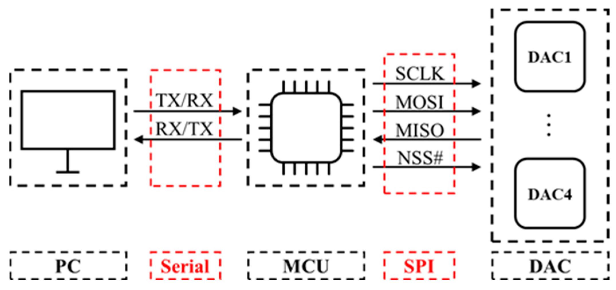
The MCU receives data packets from the personal computer through UART. These packets are parsed to extract waveform data from four independent channels and then efficiently transmitted to the DAC through specified communication protocols. Commonly used DAC communication methods include Serial Peripheral Interface (SPI), Inter-Integrated Circuit (I2C), and PWM. This paper utilizes a single-core STM32 MCU and employs a real-time operating system (RTOS) to simulate a multicore processing environment, optimizing multitask scheduling to achieve independent control of four DAC channels. While the introduction of an RTOS may lead to minor timing errors, it is essential for enhancing system performance and minimizing communication delays. This requires maximizing the communication rate between the MCU and DAC. Among these communication protocols, SPI stands out for its efficient data transmission rate and multipoint communication capability. SPI allows for the concurrent control of multiple slave devices via a single bus, offering an optimal solution for achieving multi-channel independent control of DACs when hardware resources permit. Therefore, the SPI communication protocol is prioritized to achieve high-speed and independent control of DAC, as shown in
Figure 4.
2.2. High-Voltage Amplification
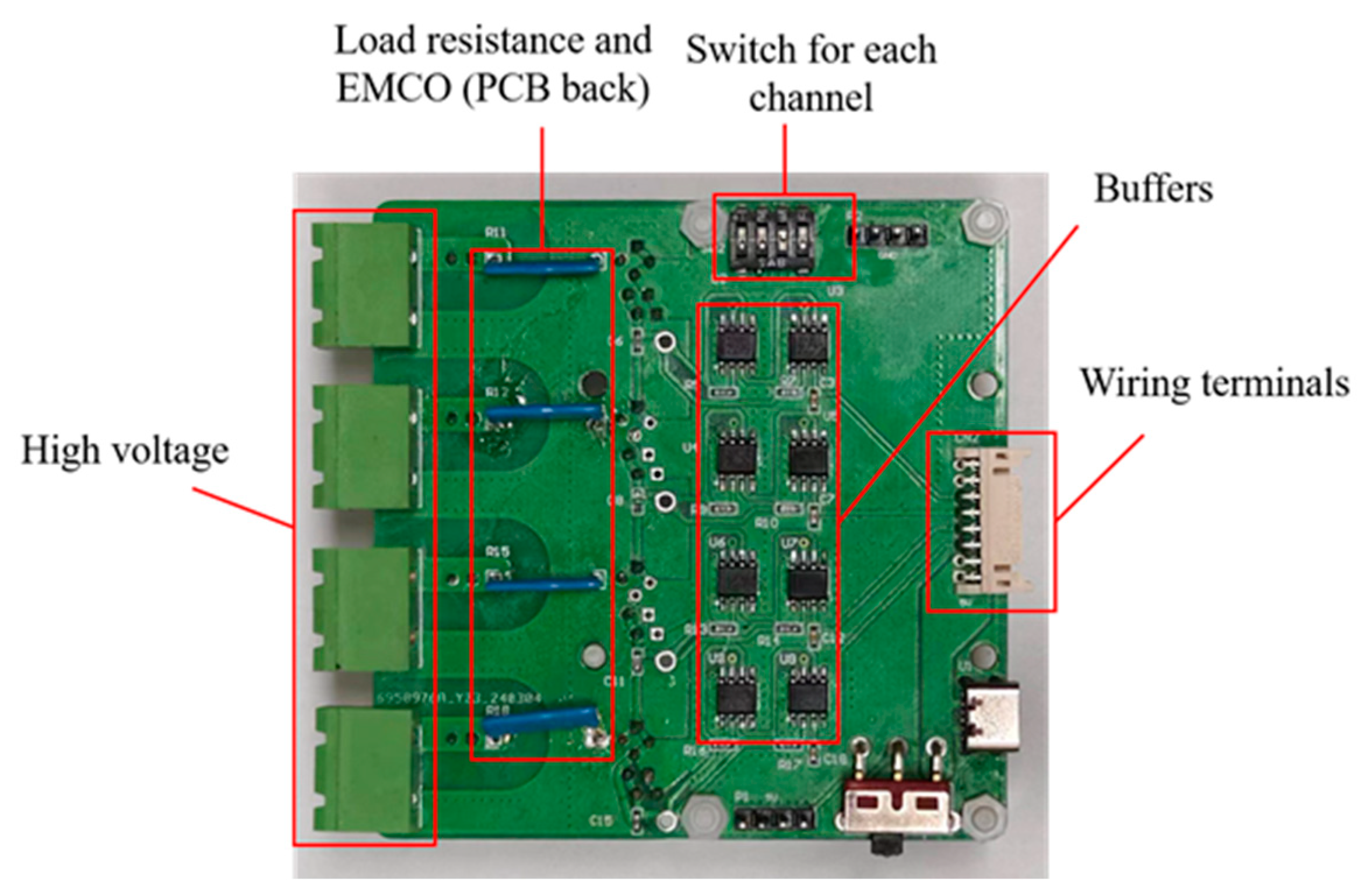
To achieve the goals of integrating and miniaturizing the driving circuit, this study has implemented an efficient integrated DC/DC conversion scheme within the voltage amplification section. The EMCO converter (A60P-5 model) from XP Power Company, a series DC/DC converter, has been chosen for its ability to amplify low-voltage input from 0.7 to 5 V by a factor of 1200, thereby achieving high-voltage output. This selection aims to reduce the number of components while ensuring high-voltage output performance. The PCB in the voltage amplification section (depicted in
Figure 5) receives four-channel signals from the signal generation section via wiring terminals. Before transmission to the EMCO converter, these signals undergo isolation and stabilization through a buffer to preserve signal integrity and stability. The inclusion of buffers aims to improve the signal-driving capability, allowing the processed signals to directly power the EMCO, thus facilitating efficient and stable high-voltage signal output.
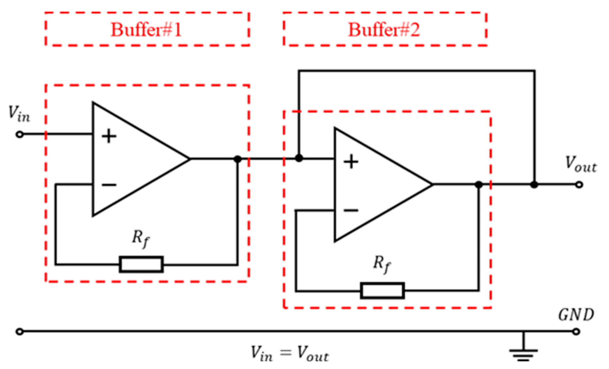
While the power consumption required to drive DEAs remains relatively low, EMCO requires a certain amount of power to sustain its operation. Direct utilization of the voltage output from the DAC to drive the EMCO may result in a decrease in signal amplitude due to inadequate driving capability. To address this concern, this study introduced a buffer amplifier to enhance the driving capability of the signal. In electronic circuit design, various methods exist to enhance voltage driving capability, such as voltage followers, emitter followers, and push-pull amplification circuits. Given the presence of internal conduction resistance within transistors and resistors, these components may affect signal amplitude during amplification. To uphold signal integrity, this paper uses a voltage follower to configure a buffer amplifier (shown in
Figure 6).
The voltage follower circuit is designed around a standalone operational amplifier, where the input signal is presented to the positive (non-inverting) input terminal, and the negative (inverting) input is tied to the output terminal. The operational amplifier’s principle of negative feedback ensures that the input and output voltages are nearly identical, with the output precisely tracking the input. Additionally, the operational amplifier’s high input impedance means it draws minimal current from the input signal, thus maintaining the signal’s original state without degradation. Considering the power demands, especially under extreme conditions that may require up to 2.5 W from the DC/DC converter, a single operational amplifier might not offer adequate power delivery capabilities. To overcome this limitation, the system employs a dual operational amplifier configuration (TLV4110 model from Texas Instruments). By cascading two of these amplifiers, each voltage follower is capable of supplying approximately 1.5 W, effectively doubling the power output and fulfilling the system’s stringent power requirements.
In the process of driving DEAs in EMCO converters, it is imperative to connect appropriate load resistors in parallel to discharge accumulated charges during the driving process, as shown in
Figure 6. The choice of load resistance significantly affects system performance. A higher load resistance slows down the discharge rate, causing a delay in transitioning the output square wave signal from high to low levels, thus extending the drop time. Conversely, smaller load resistors can expedite charge release speed and enhance waveform signal accuracy. However, they may escalate current demand, potentially exceeding the EMCO converters’s driving capacity range. Hence, optimizing the selection of load resistance is critical to ensuring effective DEA operation by EMCO converters and maintaining waveform stability. In design, achieving a balance in load resistance size is essential to meet EMCO’s maximum driving capacity while minimizing resistance value to enhance response speed and waveform signal stability. Through meticulous calculation and experimental validation, this study has determined the optimal load resistance value. This enables effective DEA driving and waveform signal optimization without exceeding the EMCO converters’s capacity.
3. Results
In this paper, the Type-C interface is used to provide power to the driver board, and successful verification is conducted to demonstrate that the designed driver circuit can autonomously generate high-voltage signals ranging from 100 V to 6000 V for each channel. The system’s programmability enables the generation of controllable high-voltage waveforms, which were subsequently tested in practical applications with DEAs. These experiments confirmed the viability of the proposed scheme through rigorous real-world driving tests. To enhance the user experience, an intuitive user interface has been developed, empowering users to easily control the output of standard waveforms through simple commands. This streamlined operational process significantly improves the ease of conducting experiments and enhances overall usability.
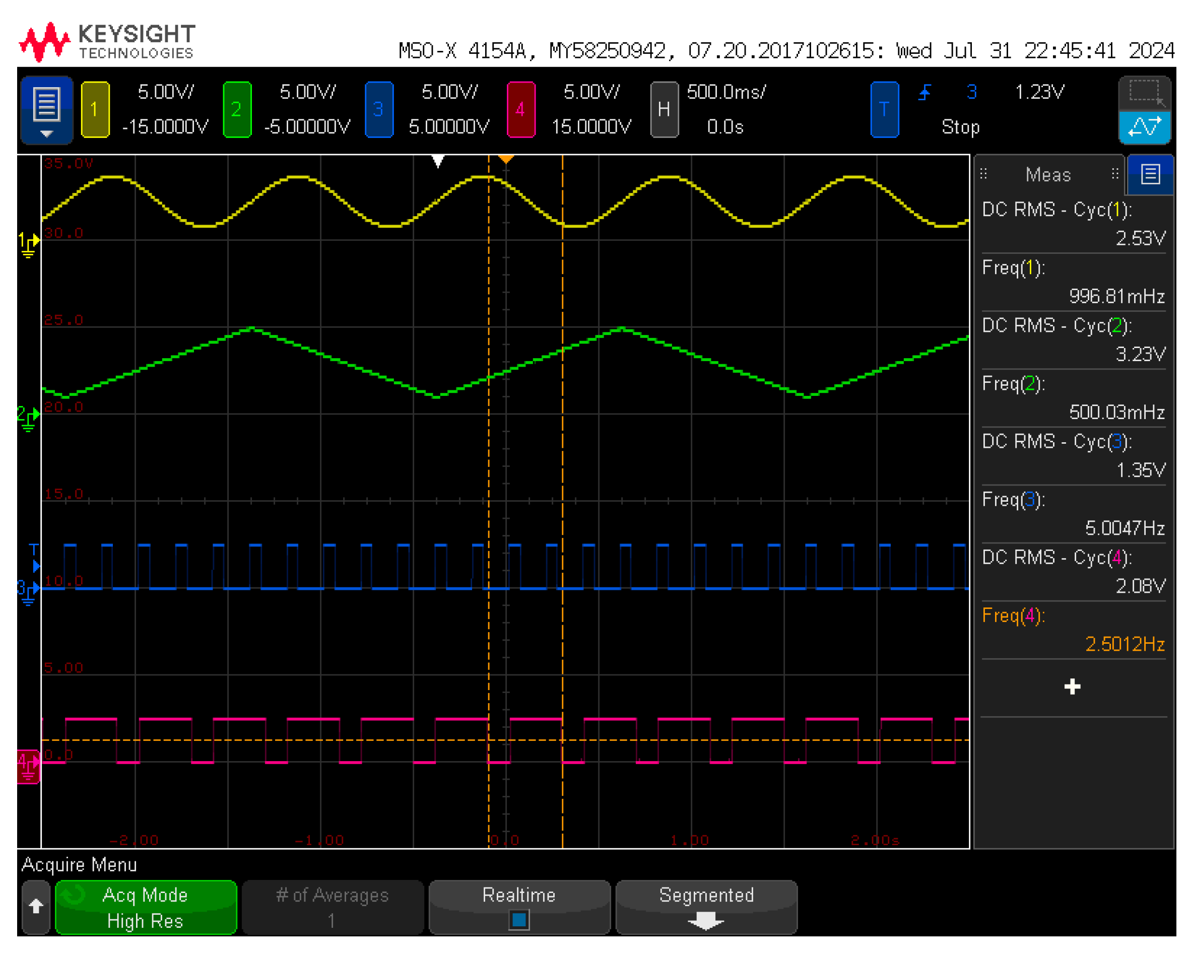
Figure 7 illustrates the capability of the signal generation component on the circuit board to produce independent signals across four channels, captured using the high-resolution mode of an oscilloscope. Each channel’s signal is sampled at 200 points per period. The yellow trace represents a sine wave, oscillating between a peak voltage of 4 V and a trough voltage of 1 V. The calculated DC effective value is approximately 2.58 V, with a frequency of 1 Hz. The measured outcomes closely align with the theoretical predictions, with any voltage discrepancies attributed to the signal fitting inaccuracies from the stepped waveform. The green trace corresponds to a triangular wave, with voltages ranging from a maximum of 5 V to a minimum of 1 V. The theoretical DC effective value for this waveform is estimated at 3.21 V, operating at a frequency of 0.5 Hz, and the actual measurements are found to be in substantial agreement with the theoretical values. The blue trace depicts a square wave with a 30% duty cycle at a frequency of 5 Hz, while the purple trace shows another square wave with an 80% duty cycle and a frequency of 2.5 Hz, featuring a high voltage of 5V and a low voltage of 0 V. The measurements for these signals are as anticipated. At the time of these tests, the signal amplification stage was not engaged, resulting in an ideal representation of the waveform signals. This confirms the efficacy of the signal generation section in producing accurate and reliable waveforms without the influence of amplification errors.
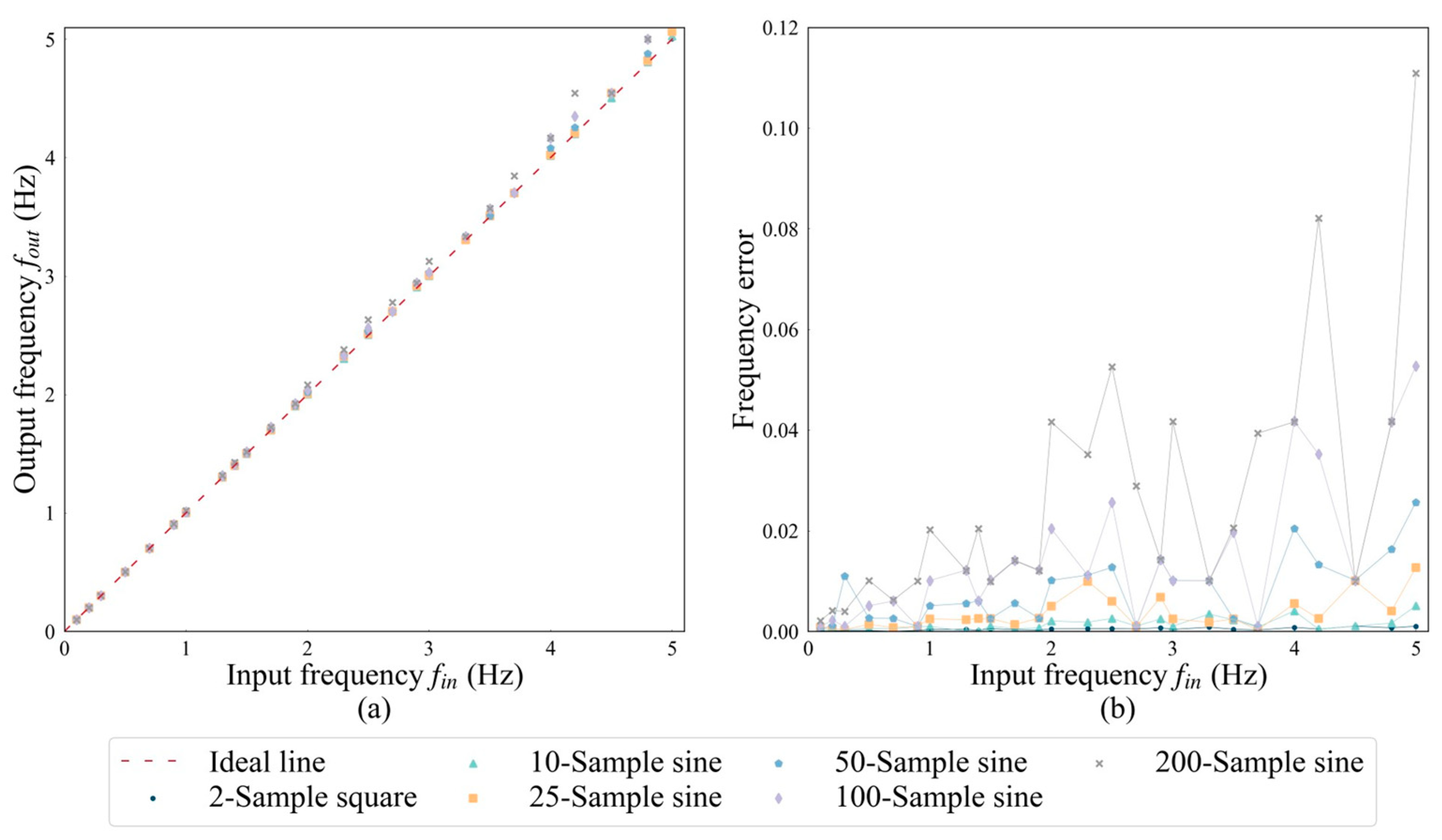
The system’s frequency error can be attributed to two primary sources. The initial source is associated with the data transmission and parsing process from the STM32 microcontroller to the DAC, which introduces a latency of approximately 35 microseconds. While this delay can be partially compensated for by adjusting the intervals between sampling points, perfect accuracy cannot be guaranteed. The resultant errors manifest in two main ways: firstly, as an increase in the output frequency above the target frequency, as depicted in
Figure 8(a), where the measured points consistently deviate above the ideal line. Secondly, as the number of sampling points per cycle escalates, the duration for data transmission and processing lengthens, amplifying the error, as illustrated in
Figure 8(b). The second source of error stems from the precision loss incurred by the internal floating-point arithmetic of the STM32 microcontroller and the RTOS clock granularity. In
Figure 8(b), despite varying sampling frequencies, a consistent error is observed at certain frequencies, exemplified by the 2.7 Hz data point where the error is uniform across different curves. The system shows fewer errors at lower sampling frequencies and corresponding input frequencies. As the input frequency increases, the error tends to amplify. Specifically, with a configuration of 200 sampling points within a single cycle at an input frequency of 5Hz, the error peaks at around 11%.
By integrating the low-voltage signals from the signal generation module with the voltage amplification module, the system can produce high-voltage signals, as demonstrated in
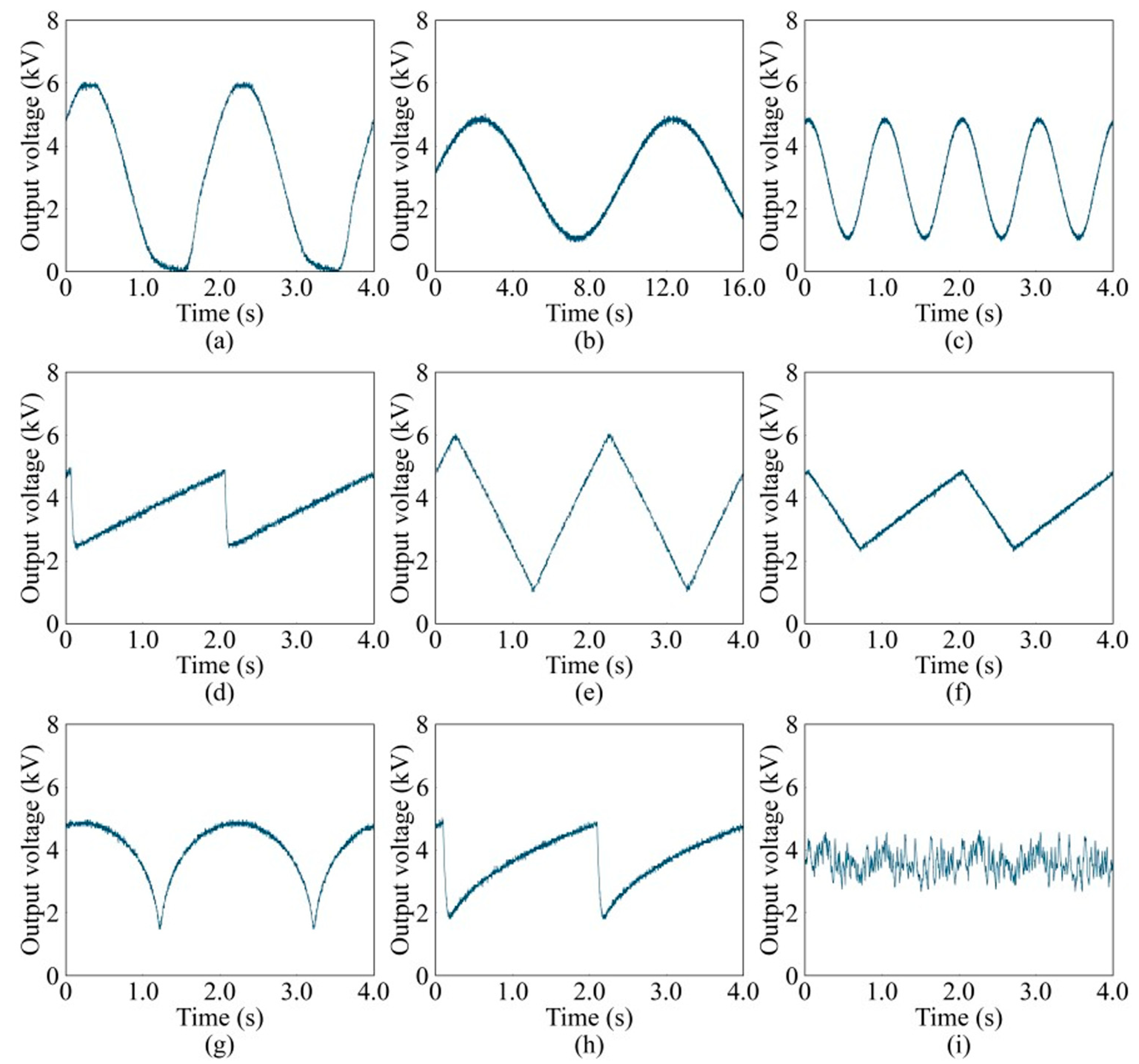
Figure 9. The captured waveforms represent a detailed profile with 200 sampling points for one cycle. Through sophisticated programming, a diverse array of high-voltage signals is output, encompassing sine waves of varying frequencies (
Figure 9(a-c)), triangular waves with distinct rise times (
Figure 9(d-f)), semi-circular arc waveforms (
Figure 9(g)), semi parabolic waveforms (
Figure 9(h)), and stochastic noise signals (
Figure 9(i)). Specifically, the sine wave in
Figure 9(a) exhibits some distortion at the lower voltage extremities, attributable to the signal’s minimum voltage level reaching 0V. When such low-voltage inputs are fed into the voltage amplification stage, they are not amplified linearly, leading to this distortion. Despite this, the system maintains its ability to generate accurate high-voltage waveforms within the operational voltage limits, ensuring suitability for a multitude of complex and demanding applications.
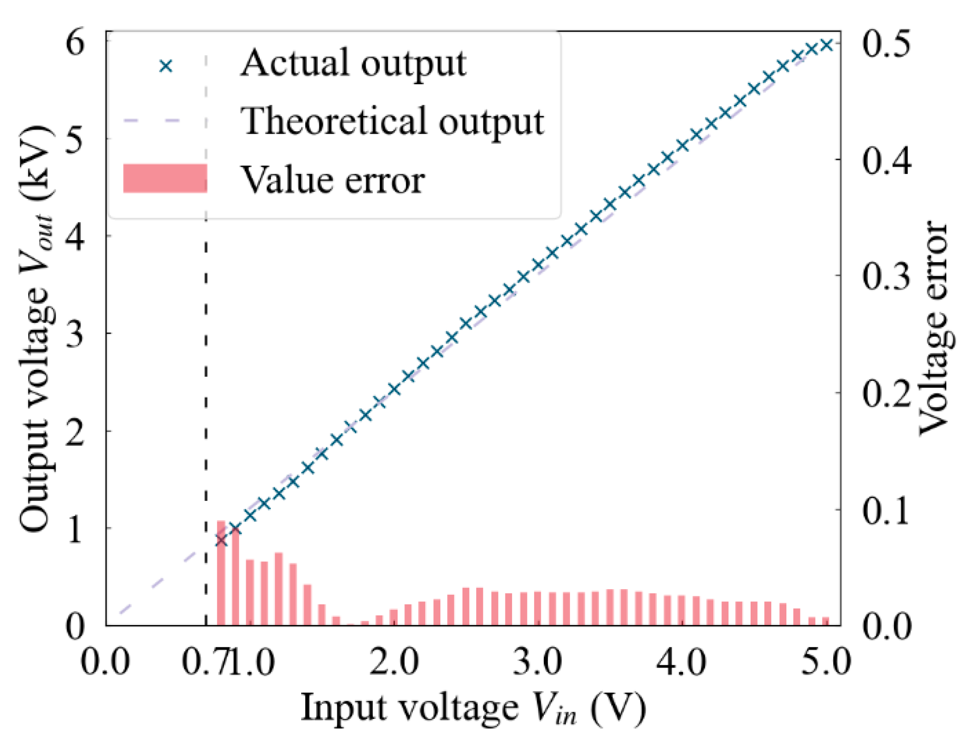
In the context of DC high-voltage signal output, this paper meticulously examined the correlation between the actual high-voltage levels produced and their theoretical counterparts, as depicted in
Figure 10, thereby quantifying the error. For inputs within the low-voltage signal range of 0.7 V to 5 V, the resultant high-voltage output is found to be largely in alignment with theoretical expectations. Within the 0.7 V to 1.3 V bracket, the error is approximately between 5% and 10%, whereas for the remaining range, it is noted to be less than 5%. The primary contributor to the high-voltage error is identified as the buffering effect on the low-voltage signal, which introduces noise that, upon amplification, escalates to the order of tens of volts.
In practical applications, programming high-voltage signals are subject to specific constraints defined by Eq (2).
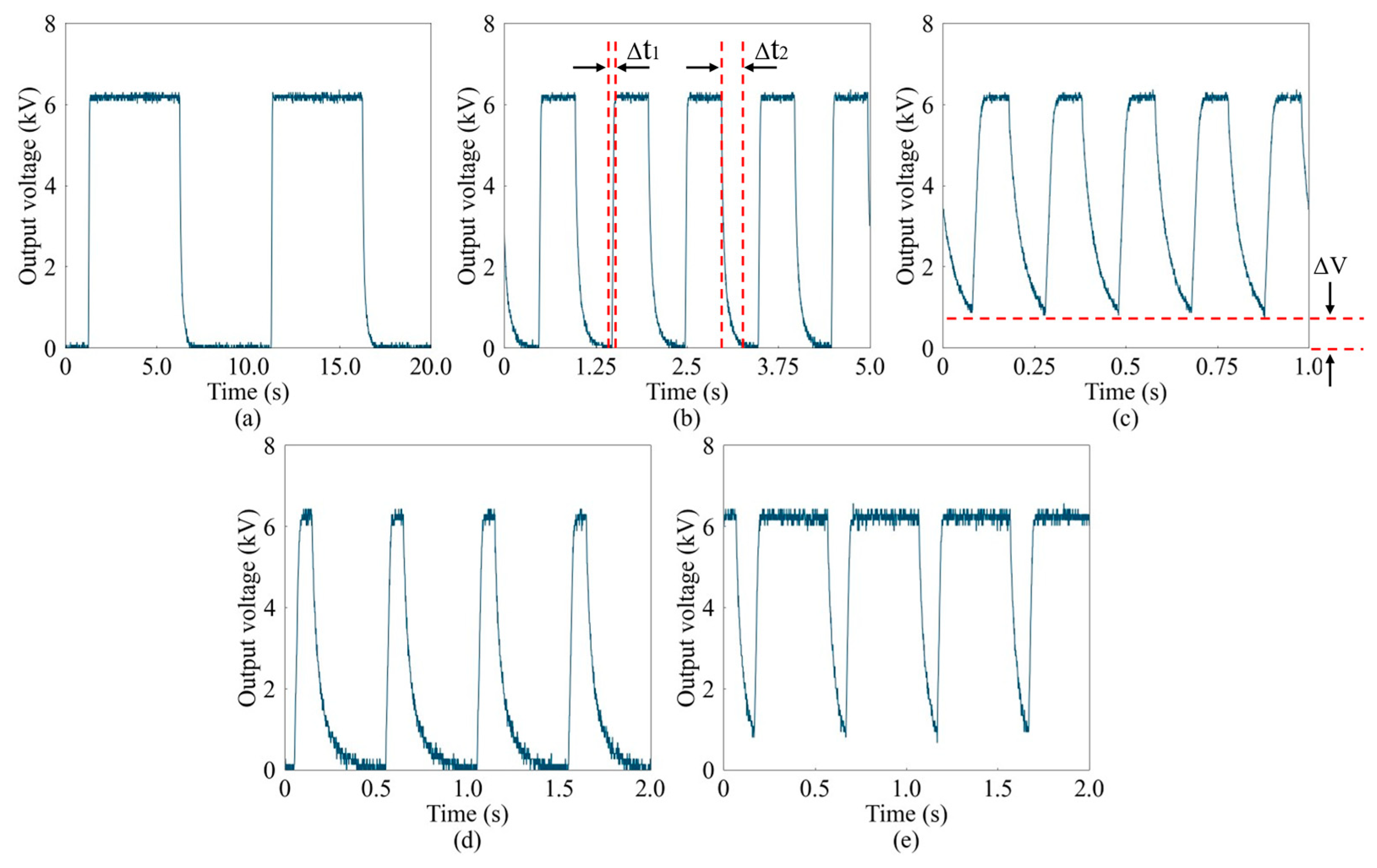
Figure 11 displays the results of tests conducted using square wave signals with varying frequencies and duty cycles, where the high level of the square wave is limited to 6 kV and the low level is 0 V. As the frequency increases, the attenuation time of the square wave signal also increases. This lengthening attenuation time is mainly attributed to the challenge of synchronizing the charge release rate with the higher signal frequency during high-frequency operation. Despite carefully selecting the load resistance during circuit design to balance power requirements, the resistance cannot be set too low, which naturally prolongs the discharge time. Additionally, the internal operations of the DC-DC converter also require a finite discharge period.
The offset voltage Δ
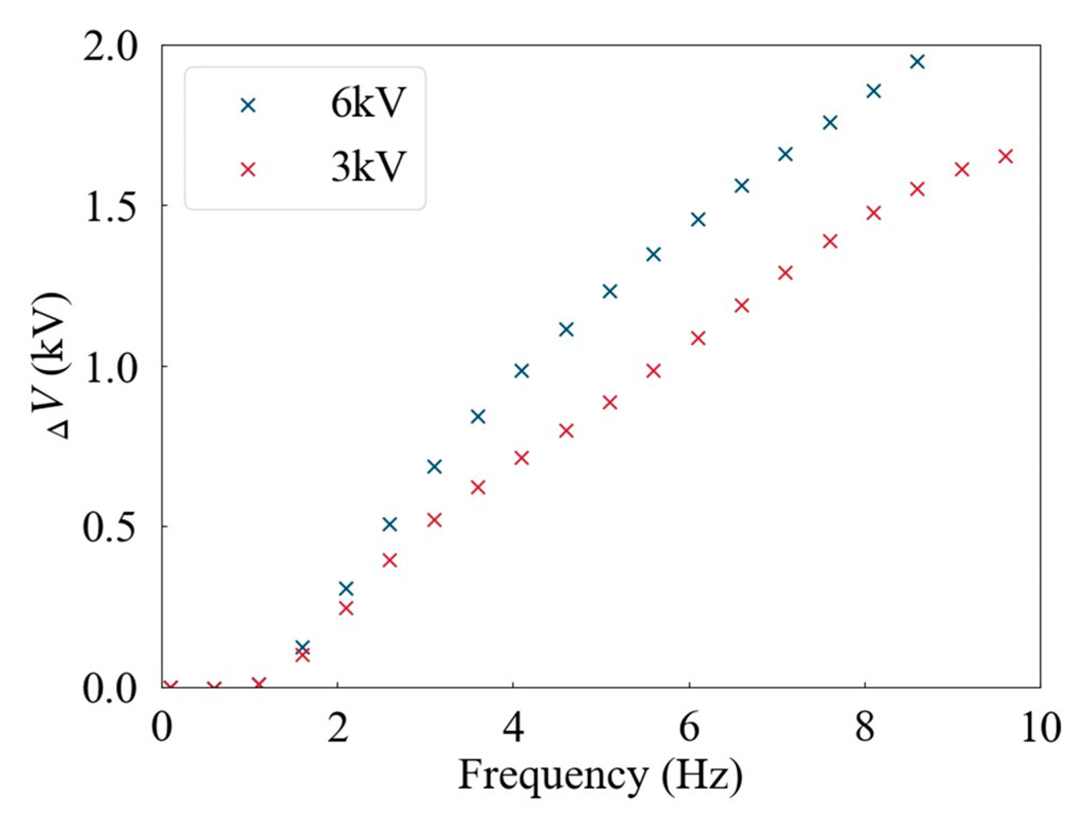
V which is the deviation of the low level from 0V under a square wave with a 50% duty cycle exhibits an upward trend as frequency increases. To precisely delineate this relationship, an exhaustive test was performed to ascertain the correlation between offset voltage and frequency.
Figure 12 illustrates the offset voltage’s dependence on frequency, plotted as a function of frequency. Consequently, when programming high-voltage waveforms, it is imperative to ensure that the voltage difference between successive sampling points adheres to the stipulations outlined in Formula 2.
This paper demonstrates the utilization of a driving circuit to transmit high-voltage signals to a dielectric elastomer actuator.
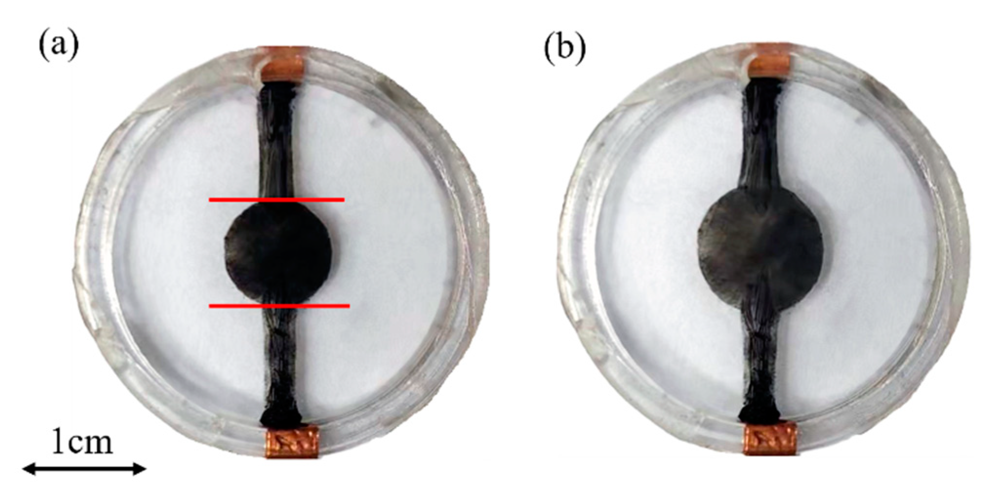
Figure 13 depicts the effect of applying a DC high-voltage signal of 3 kV to the dielectric elastomer, resulting in a significant expansion of the black electrode area in the center compared to its initial state.
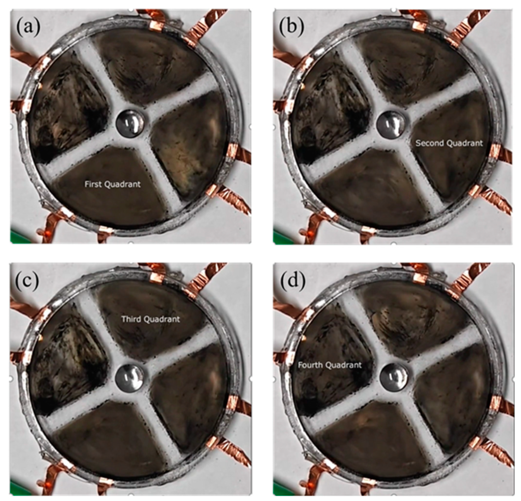
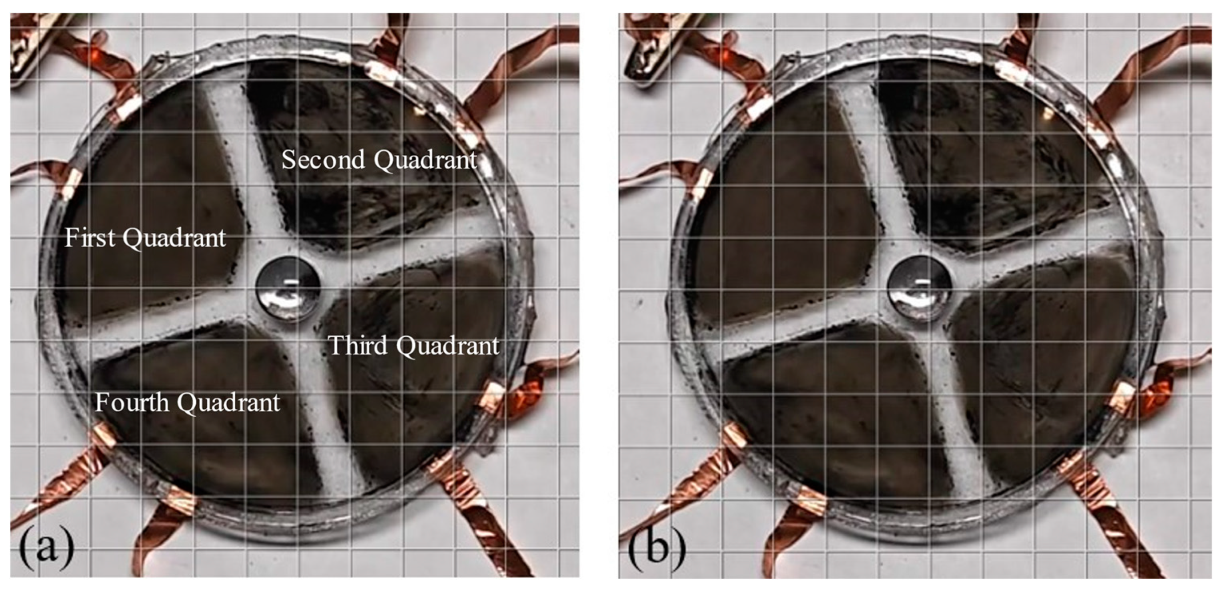
Figure 14 and
Figure 15 show-cases the separate and simultaneous activation of four dielectric elastomer channels using the circuit. Each channel experiences a square wave with a frequency of 0.5 Hz and a peak voltage of 3 kV, leading to noticeable changes in the black electrode sections in response to the applied voltage. These experiments validate the effectiveness of the circuit in efficiently driving dielectric elastomers.
To streamline the utilization of common high-voltage waveforms,
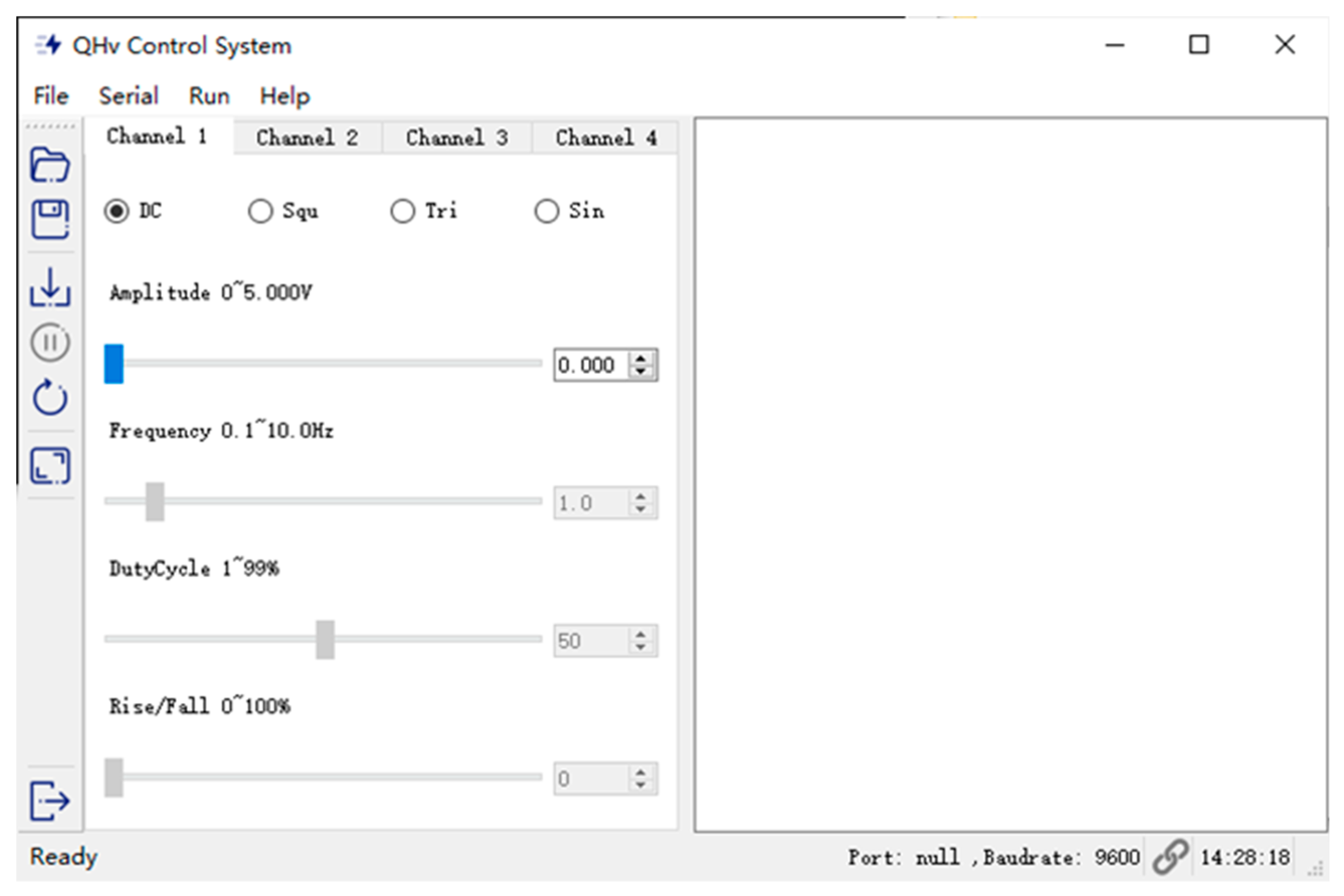
Figure 15 presents a user-friendly Python-based interface. This interface enables the circuit to output a variety of high-voltage signals, including DC, square wave, sine wave, and triangular wave, with the simplicity of basic commands. For the DC, sine wave, and triangular wave, the minimum voltage threshold is set at 100 V. Furthermore, the interface allows for the generation of other waveform signals through programmable control. Users can select an appropriate number of sampling points by specific formats to create sampling data. This data can then be transmitted to the STM32 microcontroller via the serial port, thereby facilitating the output of complex waveforms.
Figure 15.
User-friendly interface for controlling the four-channel high voltage.
Figure 15.
User-friendly interface for controlling the four-channel high voltage.
4. Discussion
Existing high-voltage power supplies for dielectric elastomer actuators often depend on commercial or self-built DC-DC converters to attain high-voltage output[
16,
17,
18,
19,
20,
21,
22,
23,
24]. These systems commonly utilize optocouplers or transistors to accurately regulate voltage levels by adjusting the duty cycle and frequency, generating a PWM (Pulse Width Modulation) signal for the high voltage. This method provides the advantages of generating high-frequency square waves and stable DC high voltage, rendering it appropriate for a broad spectrum of applications, as shown in
Table 1.
In contrast, the power supply proposed in this paper takes a new approach by directly modulating high voltage. It features a compact and simple design, facilitating the creation of a wider range of complex and diverse high-voltage waveforms. This flexibility enables it to accommodate a broader spectrum of application scenarios. Nevertheless, this innovation also reveals some limitations, especially in high-frequency operations, where frequency restrictions and the resulting high costs present significant challenges.
A key aspect of this paper is that the cost of commercial DC-DC converters, which account for over 90% of the total device costs in the proposed high-voltage power supply, could hinder its widespread adoption. These issues imply that the need for future research is to focus on the development and optimization of converters. The aim is to improve their voltage swing characteristics to better meet the demands of high-frequency driving while simultaneously working to reduce costs.
Author Contributions
Conceptualization, Y. C. and Q. H.; methodology, H.Y.X.; software, H.Y.X.; validation, H.Y.X., C.C.Y. and Z.T.Z.; formal analysis, H.Y.X.; investigation, H.Y.X.; resources, Y.C.; data curation, H.Y.X. and J.F.L.; writing—original draft preparation, H.Y.X.; writing—review and editing, Y.C.; visualization, H.Y.X; supervision, Y.C.; project administration, Y.C.; funding acquisition, Y.C. and J.F.L. All authors have read and agreed to the published version of the manuscript.
Figure 1.
Dielectric elastomer actuator working principle and structure. (a) Initial state. (b) Expanding state after applying high voltage.
Figure 1.
Dielectric elastomer actuator working principle and structure. (a) Initial state. (b) Expanding state after applying high voltage.
Figure 2.
Maxwell stress action when a high voltage is applied.
Figure 2.
Maxwell stress action when a high voltage is applied.
Figure 3.
PCB of signal generation part.
Figure 3.
PCB of signal generation part.
Figure 4.
Signal transmission in signal generation part.
Figure 4.
Signal transmission in signal generation part.
Figure 5.
PCB of High-voltage amplification part.
Figure 5.
PCB of High-voltage amplification part.
Figure 6.
Two voltage followers cascaded to form the buffer.
Figure 6.
Two voltage followers cascaded to form the buffer.
Figure 7.
The four-channel output wave of the signal generation section with (1) Sine wave. (2) Triangular wave. (3) Square wave with 30% duty. (4) Square wave with 80% duty.
Figure 7.
The four-channel output wave of the signal generation section with (1) Sine wave. (2) Triangular wave. (3) Square wave with 30% duty. (4) Square wave with 80% duty.
Figure 8.
The variation of output frequency with input frequency at different sampling frequencies, (a) measured values, (b) percentage of error.
Figure 8.
The variation of output frequency with input frequency at different sampling frequencies, (a) measured values, (b) percentage of error.
Figure 9.
High voltage waveform signal, (a) 0–6 kV sine wave at 0.5 Hz, (b) 1–5 kV sine wave at 0.1 Hz, (c) 1–5 kV sine wave at 1 Hz, (d) 2–5 kV triangular wave with full rise at 0.5 Hz, (e) 1–6 kV triangular wave with 50% rise at 0.5 Hz, (f) 2–5 kV triangular wave with 70% rise at 0.5 Hz, (g) 1–5 kV semi-circular wave at 0.5 Hz, (h) 2–5 kV semi-parabolic wave at 0.5 Hz, (i) Stochastic noise wave.
Figure 10.
Voltage response and error of the driving circuit.
Figure 10.
Voltage response and error of the driving circuit.
Figure 11.
Waveform diagrams of different square wave signals at a high voltage of 6 kV. (a, b, c): 0.1 Hz, 1 Hz, 5 Hz with 50% duty. And (d, e): 2 Hz with 20% duty and 80% duty.
Figure 11.
Waveform diagrams of different square wave signals at a high voltage of 6 kV. (a, b, c): 0.1 Hz, 1 Hz, 5 Hz with 50% duty. And (d, e): 2 Hz with 20% duty and 80% duty.
Figure 12.
ΔV increases as the frequency increases.
Figure 12.
ΔV increases as the frequency increases.
Figure 13.
Expansion of dielectric elastomer after applying voltage. (a) Initial state; and (b) State after applying 3 kV.
Figure 13.
Expansion of dielectric elastomer after applying voltage. (a) Initial state; and (b) State after applying 3 kV.
Figure 14.
The high-voltage power supply drives four quadrant DEAs separately, as shown in Supplement 1.
Figure 14.
The high-voltage power supply drives four quadrant DEAs separately, as shown in Supplement 1.
Figure 15.
The high-voltage power supply simultaneously drives four quadrants of DEAs, as shown in Supplement 2. (a) Initial state; and (b) State after applying a square wave voltage with a frequency of 0.5 Hz and a peak voltage of 3 kV.
Figure 15.
The high-voltage power supply simultaneously drives four quadrants of DEAs, as shown in Supplement 2. (a) Initial state; and (b) State after applying a square wave voltage with a frequency of 0.5 Hz and a peak voltage of 3 kV.
Table 1.
Comparison of the high-voltage power supplies in the references with that in this paper.
Table 1.
Comparison of the high-voltage power supplies in the references with that in this paper.
| References |
Control signal of waveform |
Number of channels |
Output voltage |
Output waveform |
Volume or Area |
Weight |
| [16] |
PWM |
1 |
0~5 kV |
Square/DC |
120×55×25 cm3
|
60 g |
| [17] |
PWM |
4 |
0~2 kV |
Square/DC |
5024 cm2 |
56.52g |
| [18] |
PWM |
3 |
0~16 kV |
Square/DC |
/ |
78g |
| [19] |
PWM |
1 |
0~4 kV |
Square/DC |
/ |
/ |
| [20] |
AC voltage |
1 |
0~3.5 kV |
/ |
/ |
/ |
| [21] |
PWM |
1 |
0~1 kV |
Square/DC |
/ |
/ |
| [22] |
PWM |
1 |
0~600 V |
Diversity |
/ |
1.78 g |
| [24] |
PTGD topology |
1 |
0~7 kV |
/ |
/ |
/ |
| Our work |
Programming |
4 |
0.1~6 kV |
Diversity |
80×80×50 cm3
|
62 g |
