1. Introduction
There are numerous approaches to the development of physical qubits that constitute a quantum processor, for example, those based on neutral atoms, trapped ions or most commonly superconducting charge tunneling across a pair of Josephson junctions, sometimes referred to as a Transmon. Here we consider only the latter based on its decades of research and development but note that the common challenge to all physical qubits is their fragility of the entanglement among them in the ever present vacuum noise and local interference requiring various error correction strategies that generally involve mapping many physical qubits into fewer logical qubits or logic gates [
1,
2].
Consistent with the classical computer paradigm that a “bigger” mainframe equals greater computing power at higher speeds, according to its revised quantum technology roadmap, IBM plans, by 2033, to link together multiple of its “System Two” quantum processors to form a single multi-platform system, named Blue Jay, that will include 16,632 logical qubits, 1 billion entangling gates between physical qubits and error correction modularity [
3]. For reference, one logical qubit commonly requires 1,000 physical qubits, but this depends on several factors, for instance, the error correction algorithm and the error rate.
Historically, classical computing pivoted from a mainframes-centric roadmap to one based on networked servers in the 1990’s. This led to classical supercomputers and classical data centers comprising networks of task-specific servers after the brief advent of the Cray-1 supercomputer which was essentially a highly integrated mainframe. In the present age one should expect the quantum computing paradigm to evolve from one based on large quantum processor, or cooperative multiples thereof linked internally into a single super quantum computer reminiscent of the Cray-1, to a quantum network of externally linked quantum servers. After initially exploring “more is better” as did previous generations of classical mainframe computing, a number of barriers to quantum computer scaling are becoming apparent.
Barrier 1. Quantum decoherence is a fundamental barrier in quantum computing as it refers to the loss of entanglement fidelity when a system inevitably interacts with vacuum fluctuations or thermal noise or interference in its immediate environment.
Barrier 2. Quantum Error Correction (QEC) is a vital natural response to Barrier 1 as quantum states are inherently fragile. The price for implementing QEC is an inevitable drain on qubit resources as QEC is bound by the rules of quantum mechanics.
Error detection in quantum systems must obey the quantum no-cloning theorem, which states that it is impossible to create an identical copy of an arbitrary, unknown quantum state. This rule contrasts with classical error correction, where information can be duplicated and checked for errors.
Quantum errors can occur in more ways than classical bit errors due to the nature of the qubit. For instance, a qubit error could be due to one-flip of state or a double flip to return to the original state but out of phase. This is more subtle and requires more complex error correction codes.
Barrier 3. Physical qubit number scaling does indeed scale the computational power of the processor but not in the same way as adding more transistors to a classical silicon processor. In a quantum processor, every qubit must interact with every other qubit to maximize computational power. This requirement becomes increasingly difficult to meet as the number of qubits increases. As the number of qubits increases, so does the probability for error. Errors can be introduced by anything from environmental noise to imperfections resulting from the manufacturing process, at least for qubits based on Josephson tunnel junction charge current.
Barrier 4. Formfactor of the external Input/Output (I/O) microwave links (cabling) to the outside world, [
4,
5] at least for qubits based on charge current tunneling in Josephson tunnel junction. Present packaging technology cannot scale formfactor to accommodate increasing number of output links.
Barrier 5. Six-sigma refers to the degree of control over defects and variations that a manufacturing process produces during Josephson junction qubit production and packaging. The six-sigma standard is important to achieve high manufacturing yield, reduce overhead of error correction and relax fault tolerance measures. However, six sigma scalability is limited by (1) the availability and cost of suitable materials and hardware, (2) the difficulty of controlling and connecting qubits to minimize cross talk noise, (3) the trade-off between coherence time, (roughly the half-life of a qubit) and gate speed, (generally, a fast Transmon gate is preferred as it spends less time in a noisy environment).
Barrier 6. Complexity in designing and utilizing quantum algorithms and protocols to solve a problem on a quantum computer. Complexity depends on the structure of the physical qubit, the optimization of quantum gates, the encoding and decoding of quantum information, the communication and synchronization of qubits, the verification of quantum computations and their input/output to classical bits.
Given the foregoing qualitative benefit/cost considerations of scaling the number of logical qubits per quantum processor, or the linking several quantum processors on the same platform, as indicated by the IBM quantum technology roadmap [
3], in the spirit of the “chip multiprocessor (CMP) concept prevalent in the late 20th Century,” we here
propose the concept of quantum server networks in the spirit of classical server networks that comprise classical supercomputers and classical data centers.
In this paper we propose means and methods for constructing a quantum secure network of quantum servers.
A quantum server network, as described here, comprises five basic functions.
1) Distributed small formfactor, deterministic sources of entangled photon pairs.
2) An optical fiber network over which entangled photons and encrypted classical bits streams propagate.
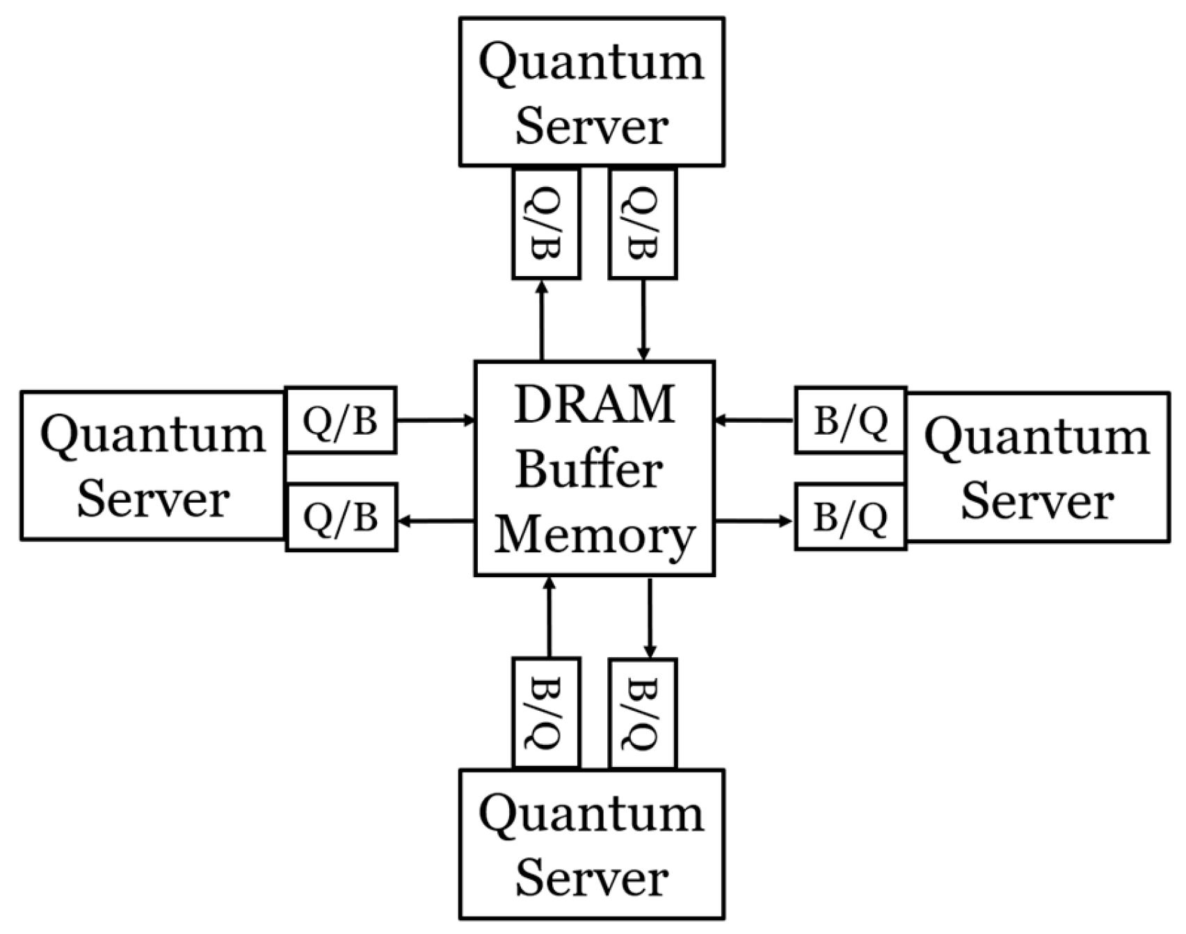
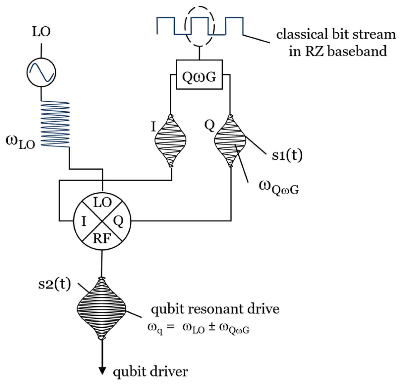
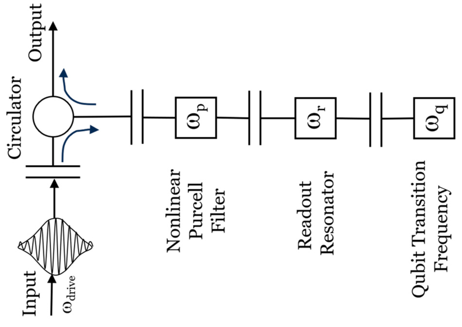
3) Classical bit to qubit (B/Q) interfaces by which classical bit streams generate streams of Transmon qubit states via a resonant qubit drive circuit as shown in Figures 8 and 9.
4) Qubit to classical bit (Q/B) interfaces by which streams of Transmon nondemolition readouts generate classical bit streams.
5) A quantum key distribution protocol, for example, the E 91 [
6], and its security analysis [
7].
The E 91 protocol of step 5) is very briefly summarized:
i) quantum dot sources that generates pairs of entangled photons on demand.
ii) sending station that prepare the entangled photons in a random superposition of two orthogonal states of polarization.
iii) sending station sends the first of two entangled photons to a receiving station.
iv) the receiving station measured the state of the received photon and records the results.
v) the sending station measures and records the quantum state of the second of the two entangled photons.
Upon the completion of several similar exchanges,
vi) the two sets of measurements are shared and compared over an insecure channel to generate the decryption key.
Compositions of In
xGa
(1-x)As quantum dots are thought to make good sources with which to generate on-demand entangled pairs of photons in the Telecom spectrum. The outstanding obstacle to this goal is the fine structure energy splitting attributed to the valence band spin-orbit coupling of the intermediate exciton level in the biexciton recombination cascade which makes the two photons correlated but not entangled because of their energy difference; see, for example [
8,
9,
10,
11]. The fine structure splitting must be sufficiently minimized to produce entangled photons having sufficiently high entanglement finesse compared to the four maximally entangled wave functions (Bell states) of two maximally entangled photon polarizations. A way to minimize the effects of spin-orbit splitting in semiconductor excitons has been theoretically understood [
12] and experimentally demonstrated in a few publications [
13,
14].
Organization of the Proposal
SECTION I describes the fabrication of deterministic semiconductor sources of entangled photons based on In
xGa
(1-x)As quantum dots comprising: (1) an optical resonator cavity to maximize photon production [
11], (2) means to locate an individual QD source sufficiently isolated from neighboring QD sources [
15,
16], (3) an anvil cell construction and operation designed to generate a shear strain in a subsurface volume that contains one and only one quantum dot source, (4) efficiently channel the entangled photon pairs generated by a specific quantum dot into a single mode Telecom optical fiber and (5) means to cryogenically cool the subject QDs to about 10 K while applying the necessary external stress.
Based on the reasonable assumption that quantum servers having just a few hundred logical qubits have a higher manufacturing yield and simpler error correction tasks, and that their coordinated problem solving may hasten the goal of reaching the ‘Practical Quantum Advantage,’ sometimes defined as the point at which quantum processors can solve problems of practical interest that cannot be solved by traditional supercomputers.
SECTION II describes a basic architecture leading to a synchronized, unconditionally secure network of modest quantum servers:
1) Secure optical fiber network for the distribution of encryption keys based on one of many quantum key distraction protocols, for example the E 91 protocol [
6] and its security analysis [
7], used “only once” for decrypting the encrypted classical bit stream sent over an unsecure channel.
2) Synchronization between quantum servers and the secure optical fiber network is possible only by the deterministic nature of the source that generates entangled photon pairs on demand.
SECTION III describes one input/output (I/O) interface scheme between a qubit and a classical bit (Q/B) and vice versa, (B/Q). A quantum server networks can be characterized by a set of separate and smaller quantum processors comprising about 100 physical qubits and about 3 k logic gates and, therefore, should have higher manufacturing yields. When judiciously linked by a quantum secure optical fiber network, a sufficiently large set of quantum servers, operating in concert, should be able to potentially achieve a performance approaching that of a large single machine endowed with a much higher qubit count but may be encumbered by massive error correction complexity. Smaller quantum processors linked in a quantum network is a concept reminiscent of classical supercomputers or classical data center networks.
By 2033, according to its revised roadmap [
3] IBM has projected that it will link together multiple System Two processors; the integrated super quantum processor will then be capable of executing 1 G gates over 2 k logical qubits. The super quantum computer ion a single platform has been given the name “Blue Jay” by its creator.
Quantum server networks can only be enabled by the development of deterministic, “on-demand,” sources of entangled pairs of photons. These sources enable photon synchronization and networking. In contrast, quantum networking and photon synchronization are not possible with probabilistic legacy sources of entangled photon pairs such as spontaneous parametric downconversion (SPDC) in various nonlinear crystals [
17] or spontaneous four wave mixing (SFWM) in a Si
3N
4 ring resonator [
18], for example. These sources exhibit entangled pair production gated by Poisson statistics.
SECTION I.
A. Constructing Arrays of InxGa(1-x)As Semiconductor Quantum Dot Sources of Entangled Photons
A source of entangled photons should have at least the following attributes:
The production of entangled photon pairs should be deterministic. This is necessary for quantum network synchronization.
The entanglement fidelity of the emitted photon pairs should be at least 95% compared with the four maximally entangled two-photon (Bell) states.
The generated pair of entangled photons should be spectrally indistinguishable and be orthogonally polarized.
The energy of entangled photon pairs should fall withing the Telecom C-band to minimize optical fiber propagation loss.
The emerging photon pairs should be entangled in the energy-time or energy-momentum degrees of freedom within the Heisenberg uncertainty limit and their provenance should be indeterminate; (there should be no “which path” information).
Manufacturing of semiconductor quantum dot sources should provide for:
Efficient harvesting of quantum entangled photon pairs into optical fiber channels.
Arrays of sources should be manufacturable at commercial semiconductor foundries.
The separation between quantum dots in an array should be of the order of 1000 – 10,000 Å to individualize a specific single quantum dot. Further separation leads to long search times.
Each source, including its cryogenic anvil cell, should have a “small” formfactor.
Several publications can be found that report work on semiconductor quantum dot sources emitting polarized pairs of photons in the optical C-band. However, while the emerging photons are often correlated to a degree, they are far from being entangled because of the influence that spin-orbit coupling has on exciton states at the valence band edge, causing differences in the energy of excitons depending on electron spin. This energy difference is seen in the exciton recombination cascade to the ground state and is termed “fine structure splitting” (FSS). FSS varies with the composition of compound semiconductor quantum dots, and is particularly large in InxGa(1-x)As. Non-degeneracy of light emitted during the recombination cascade will violate one of the conditions for entanglement, to wit, energy indistinguishability.
The spin–orbit interaction is a relativistic interaction of the electron spin with its orbital angular momentum. Spin-orbit coupling has a significant effect on the band structure, particularly at the valance band edges where the exciton energy levels reside.
Cumulative internal strain stemming from naturally occurring or designed lattice mismatch, for example, designed metamorphic strain as part of bandgap engineering, or an externally applied stress introduces additional coupling between the heavy-hole (HH) bands, light-hole (LH) bands, and the spin-orbit split-off (SO) bands. Such coupling can be useful, for example, in partially or wholly negating the effects of sub-band exciton energy splitting in cascade recombination emission. This is the case for excitons in metamorphic lattice-matched systems such as AlxGa(1-x)As/GaAs and InxGa(1-x)As/GaAs, the latter being of interest here.
The theory of the effects of shear strain on spin-orbit valence band edge energy levels, and experimental verification as it applies to exciton level splitting can be found in part in [
12,
13,
14].
Fabrication practices by which to control the density of quantum dots can be found, for example, in publications [
15,
16].
The construction of an optical resonator cavity suitable to produce efficient emitters of entangled photon pairs from a semiconductor quantum dot may be found, for example, in publication [
11].
Significant early results on the effect which an externally applied stress has on the fine structure splitting in the exciton emission cascade from InGaAs quantum dots is reported in [
19].
In addition to the attributes listed above, a deterministic quantum dot source of entangled photons, must be based on:
An optical resonator cavity to maximize photon production [
11].
Means to locate the individual QD source, isolated from neighboring QD sources, [
15,
16].
An anvil cell with which to generate a shear strain in a subsurface volume of a quantum layer that contains the quantum dot source
Efficient channeling of entangled photon pairs generated by a specific quantum dot into a single mode Telecom optical fiber, and
Means to cryogenically cool arrays of anvil cells containing quantum dot sources to about 10K.
B. Optical Resonator Source Fabrication
Depicted in
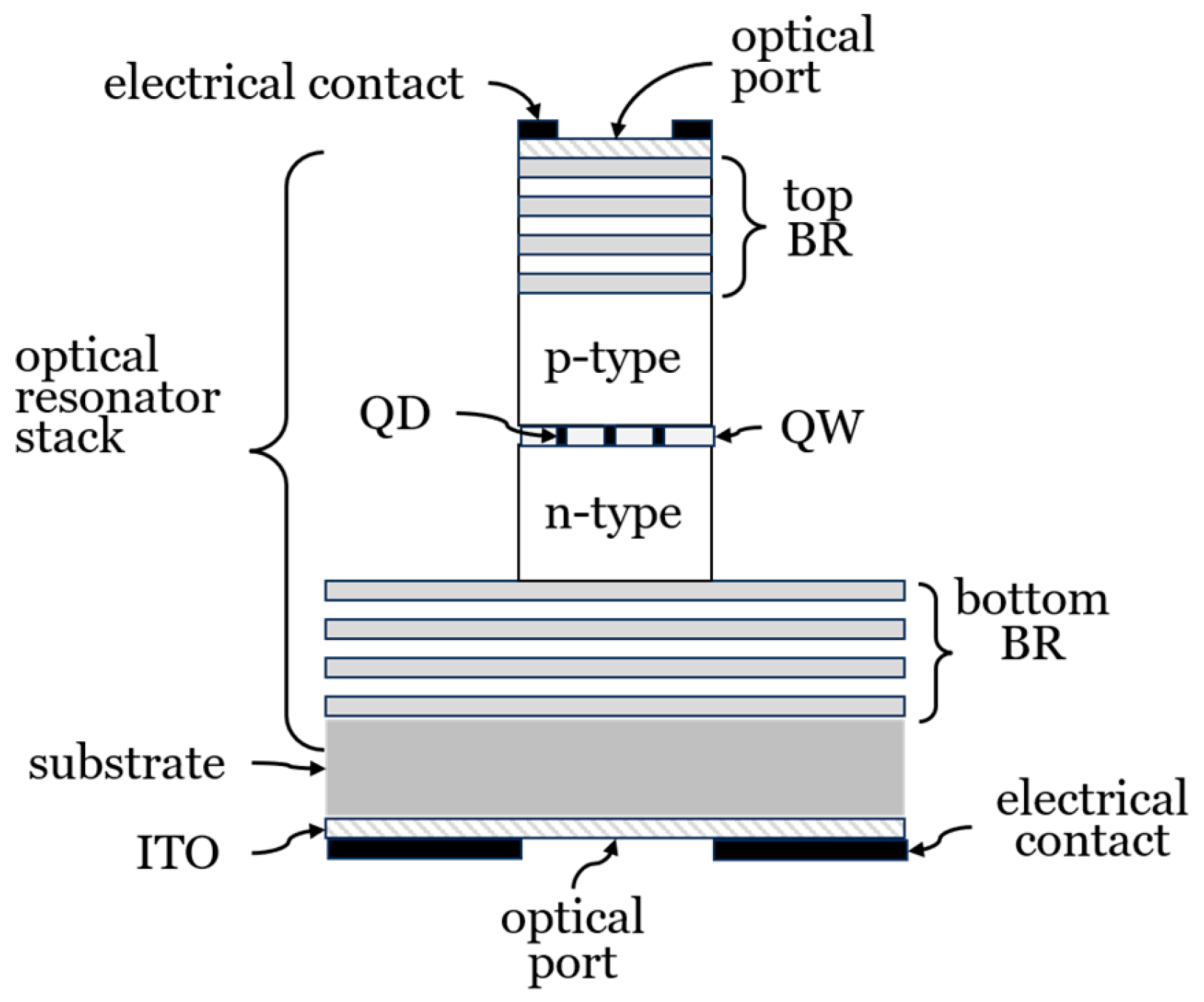
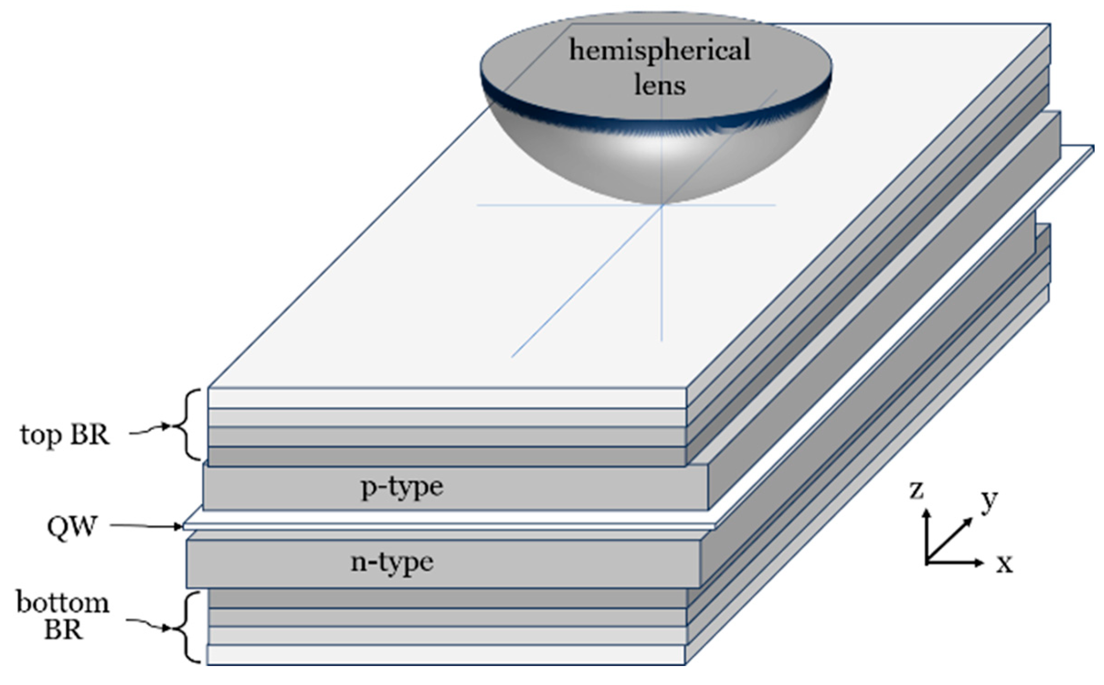
Figure 1 is a stack of compound semiconductor layers comprising an optical field micro-cavity resonator substantially similar to those commonly found in ubiquitous Vertical Cavity Surface Emitting Lasers (VCSELs) and discussed in reference [
11]. It is noted that VCSELs are generally used in short distance optical communications over multimode optical fibers and generally operate at wavelengths in the 850 nm range where semiconductor compound compositions can be found to simultaneously offer 1) good lattice matching and 2) indices of refraction with sufficiently high contrast so that the number of layers in the top and bottom Bragg grating reflectors, that define the optical resonance cavity, can be kept to a minimum and still achieve a resonator cavity with sufficiently high quality factor.
Unfortunately, these fortuitous advantages are greatly diminished in the optical C-band where a substantially larger number of Bragg grating reflector layers, top BR and bottom BR, are needed to achieve a substantially adequate resonance finesse.
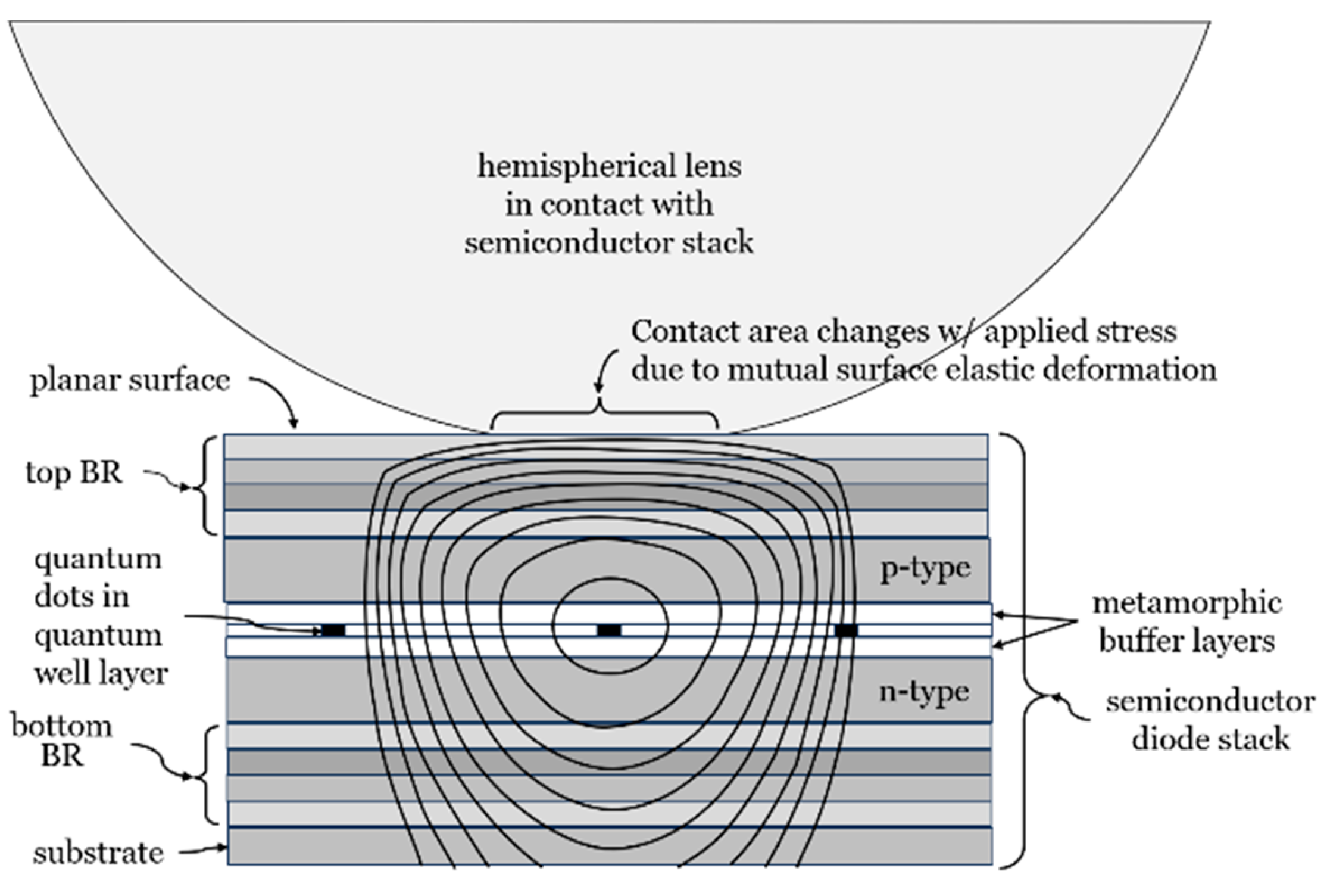
Quantum dots (QD) are fabricated in a semiconductor quantum well (QW) layer between a p-type and an n-type cladding layers, generally built on a GaAs substrate. It is noted that the structure is, in fact, a semiconductor diode having top and bottom electrical contacts.
A top and bottom thin layer of optically transparent Indium Tin Oxide (ITO) alloy of composition In
(2-x)Sn
xO
3, may be added to promote uniformity in the applied electric bias field. A bottom optical pump port is added to facilitate optical excitation of quantum dots whose fluorescence emission may be used to locate a single quantum dot in a sparse quantum dot field. A system designed to generate and align entangled photon emissions from a specific quantum dot for the purpose of deterministically generating, entangled photon pairs and channeling them into output optical fibers is shown in
Figure 2,
Figure 3 and
Figure 4 and 7.
C. Anvil Cell and Entangled Photon Harvesting
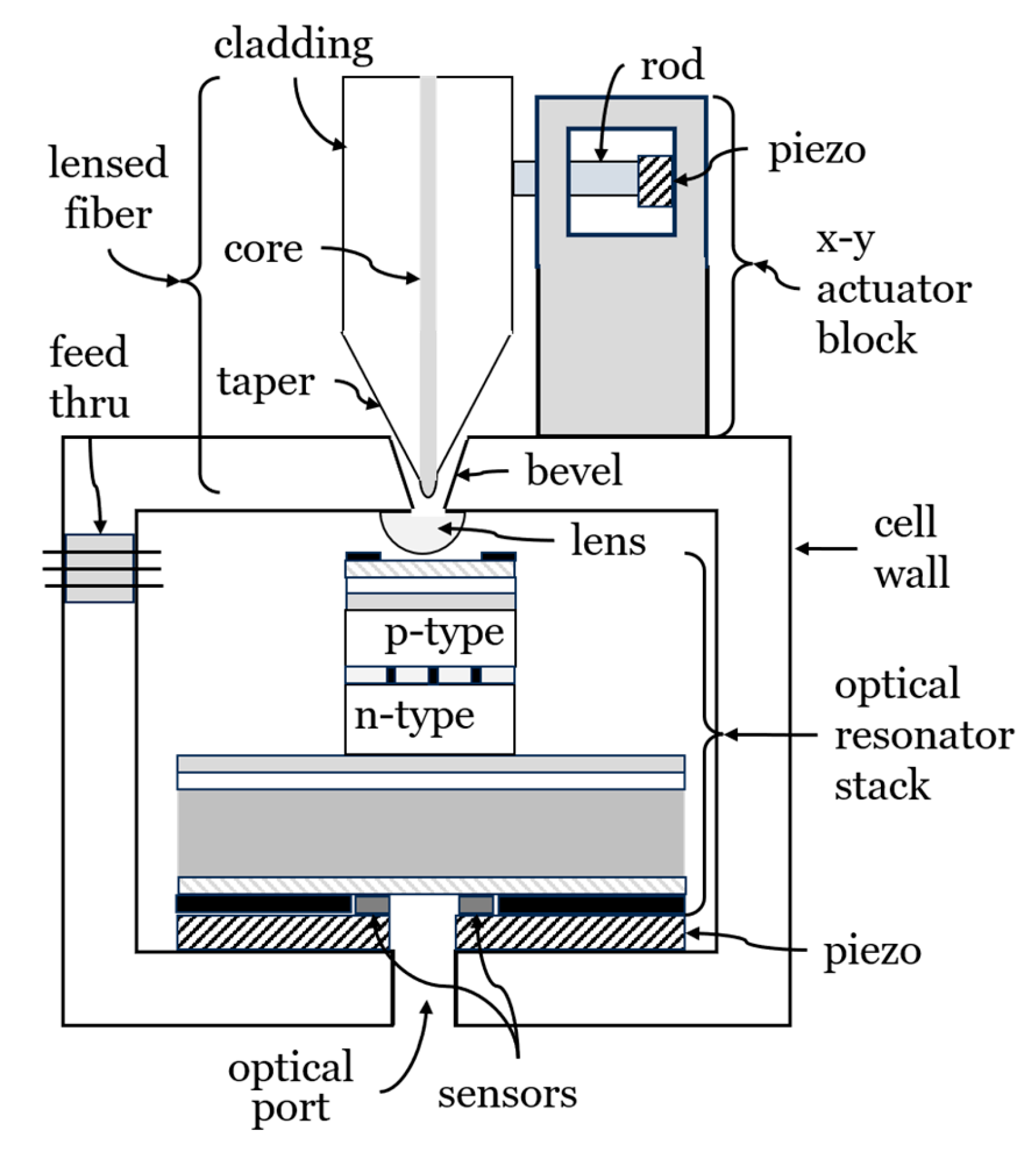
The primary purpose of the anvil cell is to generate a shear strain in a subsurface volume that contains the quantum dot source. The magnitude of the shear volume must be sufficient to sufficiently reduce the indistinguishability of the emitted entangled photon pairs. The cell wall enclosure provides the elastic spring constant restoring force that opposes the compressive stress produced by the piezoelectric actuator that pushes the semiconductor stack, shown in
Figure 1, against the hemispherical lens. Emitted photons exit the top port and are channeled into an optical fiber by the hemispherical lens into the core of a lensed optical fiber. An x-y actuator block is used to align the lensed fiber while feed-thru electrodes provide diode electrical bias, piezoelectric actuator power and sensor I/O.
Depicted in
Figure 2 is an anvil cell design whose purpose is to produce subsurface shear strain in a small volume
v, that includes the target quantum dot located at a distance
d, below the surface of the semiconductor stack shown in
Figure 1. The volume
v and subsurface distance
d, are nonlinear functions of the radius of the hemispherical lens, the applied force generated by the piezoelectric actuator (piezo), the effective spring constant of the anvil cell enclosure, the moduli of elasticity and Poisson ratios of each the hemispherical lens and the optical resonator stack. These determine the diameter, 2
r, of the contact area shown in more detail in
Figure 6. In the elastic limit the contact area should reversibly deform with applied stress whose magnitude can be monitored with stress sensors.
It is noted that the key parameters 2
r,
d and
v can be computed quasi analytically and is the subject of the theory of Hertzian contact stress, an excellent review of which may be found beginning with page 1658 in publication [
20].
Emitted entangled photon pairs can be channeled into an external output optical fiber by a lensed optical fiber.
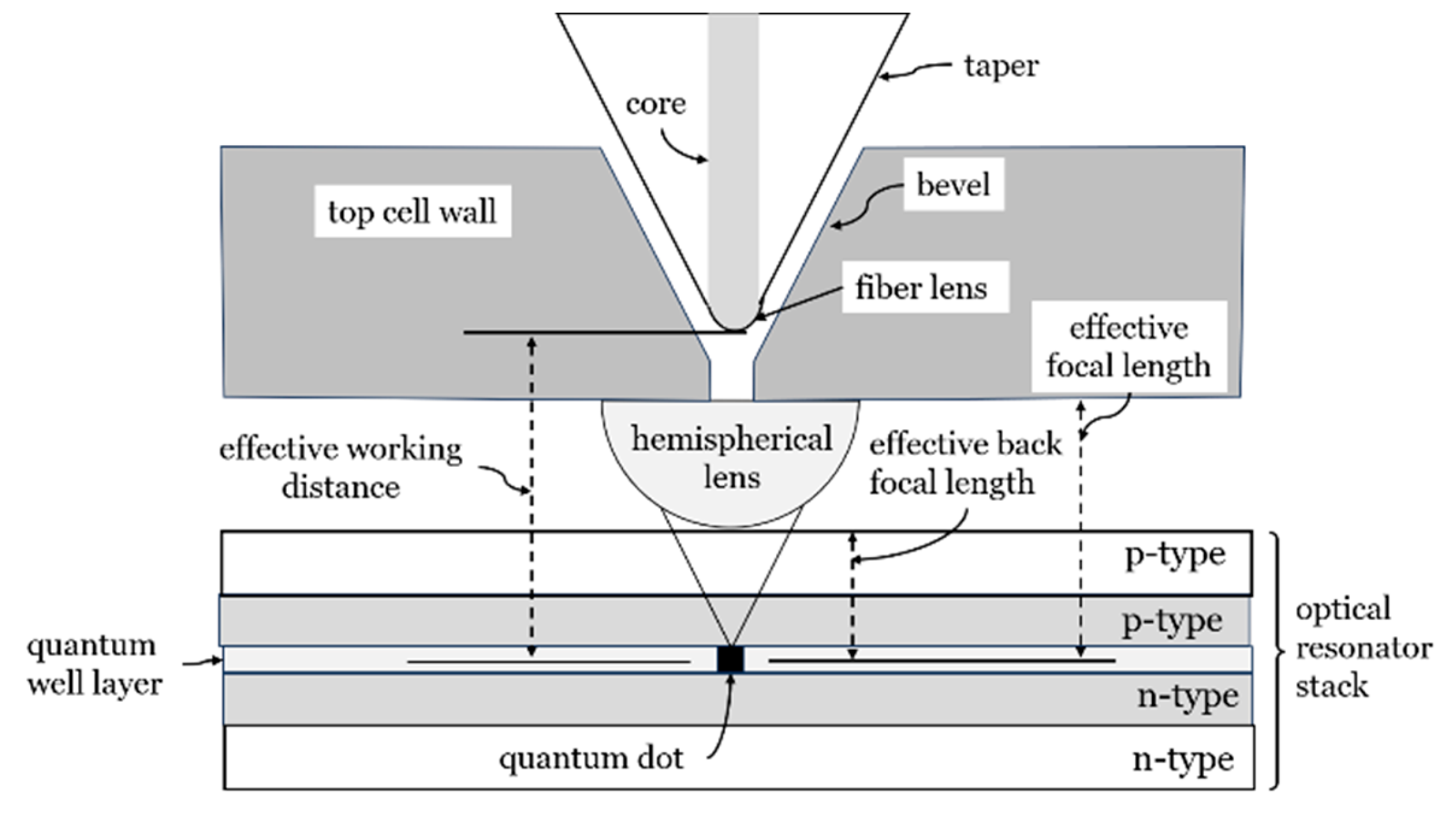
Figure 4 shows, in more details the role of components directly related to coupling emitted photons to an external optical fiber through a bevel access port in the anvil cell; in particular the role of the internal hemispherical lens which also serves to generate the subsurface shear strain field. The purpose of the bottom optical access port is explained in conjunction with
Figure 1.
The hemispherical optical lens has the dual purpose of aiding in channeling the emitted entangled photon pairs into the external optical fiber and to provide subsurface shear strain. Lens materials having sufficient mechanical hardness, vis a vis the semiconductor stack and high transparency in the optical C-band are, for example, fused silica and Al2O3.
The electrical feed thru provides low bias voltage to the optical resonator cavity diode stack, high bias voltage to drive the piezoelectric actuator providing external stress and I/O signal/power to the calibrated force sensors. The beveled access hole on the anvil cell top wall provides lensed fiber access.
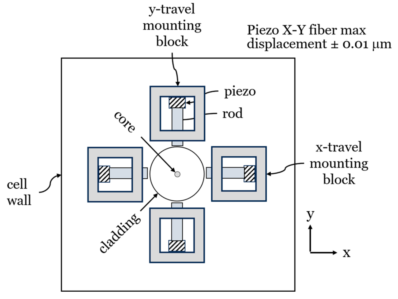
The x-y actuator block attached to the top wall of anvil cell provides fine optical fiber alignment in the x-y plane to locate a specific quantum dot and optimize the collection of entangled photon pairs therefrom.
D. Lensed Fiber Fine Positioning
Once a quantum dot is selected, for example, by locating its fluorescence emission under optical pumping through the bottom optical port in the anvil cell, its location is more precisely ascertained by moving the lensed optical fiber in the x-y plane orthogonal to the quantum well layer containing the quantum dot. This is accomplished by the piezoelectric actuators mounted on the anvil cell top wall used to minimally translate the lensed optical fiber.
E. Quantum Dot Source to Optical Fiber Photon Channeling
In
Figure 4 only that portion of the top wall of the anvil cell that contains the bevel access port that enables access to the lensed optical fiber is shown. The clearance between the bevel cut and lensed fiber enables alignment of the lensed fiber in the x-y plane by means shown in
Figure 3 and intended to optimize the collection efficiency between a quantum dot emitter and the collecting optical fiber core with the aid of a hemispherical lens which is also used to generate the subsurface shear strain. Important distances to consider in a first order optical simulation are shown as 1) the effective working distance from the plane of the quantum dot to the tip of the lensed fiber, 2) the effective focal length from the planar surface of the hemispherical lens to the plane of the quantum dot, and 3) the effective back focal length from the tangent to the hemispherical lenses’ curved surface to the plane of the quantum dot.
Several optical simulators are commercially available with which to simulate the light collection efficiency of combinations of the various parameters. For example, Ansys Optics and Photonics Simulation Software.
F. Subsurface Generation of Maximum Shear Strain
Figure 5 is a less detailed perspective representation of the structure depicted in
Figure 1.
Contours in
Figure 6 are meant to represent surfaces of constant shear strain. Contained smaller contour area correspond to higher in magnitude in a smaller volume under conditions of applied constant external stress. The volume of maximum shear strain can be designed to coincide with a volume that contains a single quantum dot by means summarized in conjunction with
Figure 2 and
Figure 4. It should be noted that the formalism used to describe the shear strain generated during the application of an external compressive stress between two objects whose surfaces are in mechanical contact is based on the elastic limit of all components. For example, the depth,
d, of maximum shear train below the flat surface is estimated as
Figure 6.
Hertzian theory of contacting surface. Depicted is a side view of the drawing in
Figure 5 emphasizing a rendition of subsurface shear strain contours resulting when a spherical surface is in compressive contact with a planar surface [
20,
21,
22].
Figure 6.
Hertzian theory of contacting surface. Depicted is a side view of the drawing in
Figure 5 emphasizing a rendition of subsurface shear strain contours resulting when a spherical surface is in compressive contact with a planar surface [
20,
21,
22].
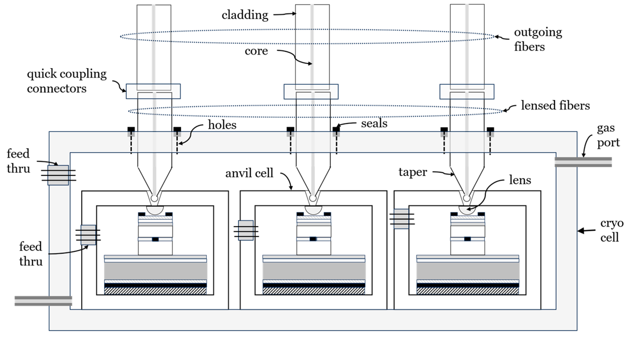
G. Cryogenic Assembly of Quantum Dot Sources of Entangled Photons
Figure 7 depicts one approach for increasing the throughput of a quantum information network by taking advantage of plural deterministic and synchronized sources of entangled pairs of photons. In the figure is shown an array of anvil cells each hosting an activated quantum dot in a quantum well layer while being coupled to a lensed optical fiber. A cryogenic enclosure keeps all anvil cells contained therein within a desired range of temperature by continuously flowing cold gases through I/O gas ports. A closed-cycle cryostat may provide cooling gases at about 10 K. Lensed optical fiber arrays couple streams of entangled photon pairs from quantum dots sources to matching outgoing optical fiber arrays by means of standard single mode optical fiber quick couplers/decouplers. Cryogenic seals minimize loss of cooling gas through optical fiber access holes. Electrical feedthroughs provide power and sensor I/Os as needed.
