1. Introduction
Formulating a precise definition of ’energy transition compatible with sustainable development’, not only from a strictly environmental point of view, is not an easy task. In fact, the concept changes depending on numerous factors such as geographical, environmental, social and economic. However, it is possible to give a definition of this process in a generic and commonly acceptable way as the ’gradual change of society and the economy towards sustainable actions from an environmental, social and governance point of view’. The UN has addressed this topic numerous times since the 1980s (i.e. in the Brundtland Commission) and has universally described and structured the problems underlying the concept of sustainable development; see ’UN Agenda 2030’ [
1]. The problems that need to be addressed to carry out a gradual transition are numerous, not all of them are easily solvable, and even some of them have not yet been outlined in their particular characteristics; for example the criteria for the objective measurement of sustainability in the industrial sector and even less in the civil and domestic spheres have not yet been defined, and a precise definition of the parameters with which to arrive at an objectively comparable model is still missing [
2,
3].
In Europe the ESG European Institute Commission is an organization whose objective is to define and suggest the criteria for sustainable development also from an economic and financial point of view, however this is a difficult task due to the difficulty of building a taxonomy of all categories involved in these processes. If on the one hand it is clear that it is necessary to address the problem from a global point of view, on the other hand it must be taken into account that the scenario is extremely heterogeneous given that the social, economic and cultural conditions are extremely different. In Europe there is an intense debate on how to address these problems and above all with what speed to boost the transformations that imply the removal of the dependence of energy production on fossil fuels. As mentioned, sustainable development cannot only be framed in an ecological context, but also considering important social and governance aspects. If we made the mistake of considering only one of these areas, there could be serious consequences and negative repercussions on the others [
4].
However, aside these general considerations, that we consider as a point of reference for our actions, one of the tasks of technicians and researchers is certainly to try to remove the obstacles that can make it difficult to adopt systems useful for the sustainable development process. Just some important areas in which research is engaged, studying innovative solutions that facilitate the transition at least from a technical and technological point of view, are: the improvement of the energy efficiency of production from renewable sources; the reduction of costs of the equipment and their installation; the ease of use; the security; the duration and reduction of their environmental impact; the compatibility with other conversion systems connected to the same grid.
Through the interactions with companies producing PV systems, and with users and potential users, some needs of a technical nature have emerged which pushed us to identify solutions that can satisfy the requests. Many of these technical aspects concern the quality of the output voltage of DC/AC converters from photovoltaic sources that connect both to the electrical grid and to isolated grids. In particular, some specifications concern the stability in frequency and voltage amplitude on isolated grids, while on prevalent power grids problems have been highlighted regarding the current ripple affecting the output filters. This circumstance often makes it difficult to design this stage respecting the limits of both conducted and radiated electromagnetic compatibility and therefore following the rules dictated by the standards as well as in the specifications imposed by the operator of the electricity line.
From a more general point of view, further problems are highlighted, very often unintentionally overlooked by both conversion system manufacturers and users. One of these is the high harmonic content, both at high frequency and at frequencies lower than 50 Hz, introduced into electrical grids and which often propagates causing unpredictable effects [
5]. Dangerous interactions with other conversion systems can occur, generating potential situations of latent instability; they can be triggered by particular events such as the disconnection or connection of a branch of the electricity grid, or the onset of a fault [
6,
7].
A further requirement has been reported which concerns the voltage supplied by the panels and strings of photovoltaic panels. In particular, it is frequently considered useful to have conversion systems capable of operating on relatively low DC voltages, for example around 100V, in order to create very low voltage strings made up of several elements in parallel, each composed of no more than one pair of panels in series that can achieve a peak voltage rating of 120V.
The main guidelines to follow for the design of a conversion system that meets the mentioned needs can be summarized as follows:
Possibility of connection to isolated grids and distribution grid;
Connection to a very low voltage photovoltaic system, not exceeding 120V;
Drastic scaling of reactive elements;
Improved performance in terms of harmonic content injected in the grid;
Improvement of the overall reliability of the conversion system;
Less susceptibility of the control system to grid disturbances, with particular regard to phenomena known as "harmonic stability" and greater robustness in terms of ability to contribute to grid
Following the indicated criteria, a critical analysis is carried out aimed at identifying the most suitable conversion topology, considering and comparing both classic and less conventional configurations. From the studies reported in the bibliography, but also from the experience gained in the design of CSI converters, some important differences, among all types, emerge with strong evidence.
1.1. Structure of paper
The structure of the paper follows the design logic that was followed allowing to arrive at the final topology of the conversion system.
The design solutions present in the literature based on both VSI converters and CSI converters were considered by evaluating their respective characteristics and performances, as well as their adequacy with respect to the specifications set on the maximum voltage of the photovoltaic system and on their ability to interface with both a standard distribution grid or an insulated grid.
Section 2 reports the considerations that led to the choice of a CSI conversion bridge, while
Section 3 describes the modulation technique used in the CSI bridge and the implementation method.
Section 4 considers a possible promising conversion solution, for the DC/DC conversion stage, in terms of voltage step-up capacity. In order to verify its performance and establish its ability to respond to the established specifications, some simulations were carried out which allowed it to be characterized. The data provided by these simulations suggested introducing some modifications to the DC/DC stage that allowed to significantly improve its step-up capacity and to eliminate the fourth leg of the CSI bridge. The same Chapter describes the modulation technique adopted for this stage and the related synchronization technique with the CSI bridge.
Finally,
Section 5 reports the data relating to the simulation of the entire model, without controls of the output voltage (in the case of an isolated network) or the output current (in the case of connection to the distribution network), in this case the module and the phase of the CSI reference current were set to constant values. Likewise, the model is not equipped with current control of the DC/DC stage since the Duty-Cycle has been set at a constant value.
2. Issues and Advantages of Conversion Systems Based on CSI
The
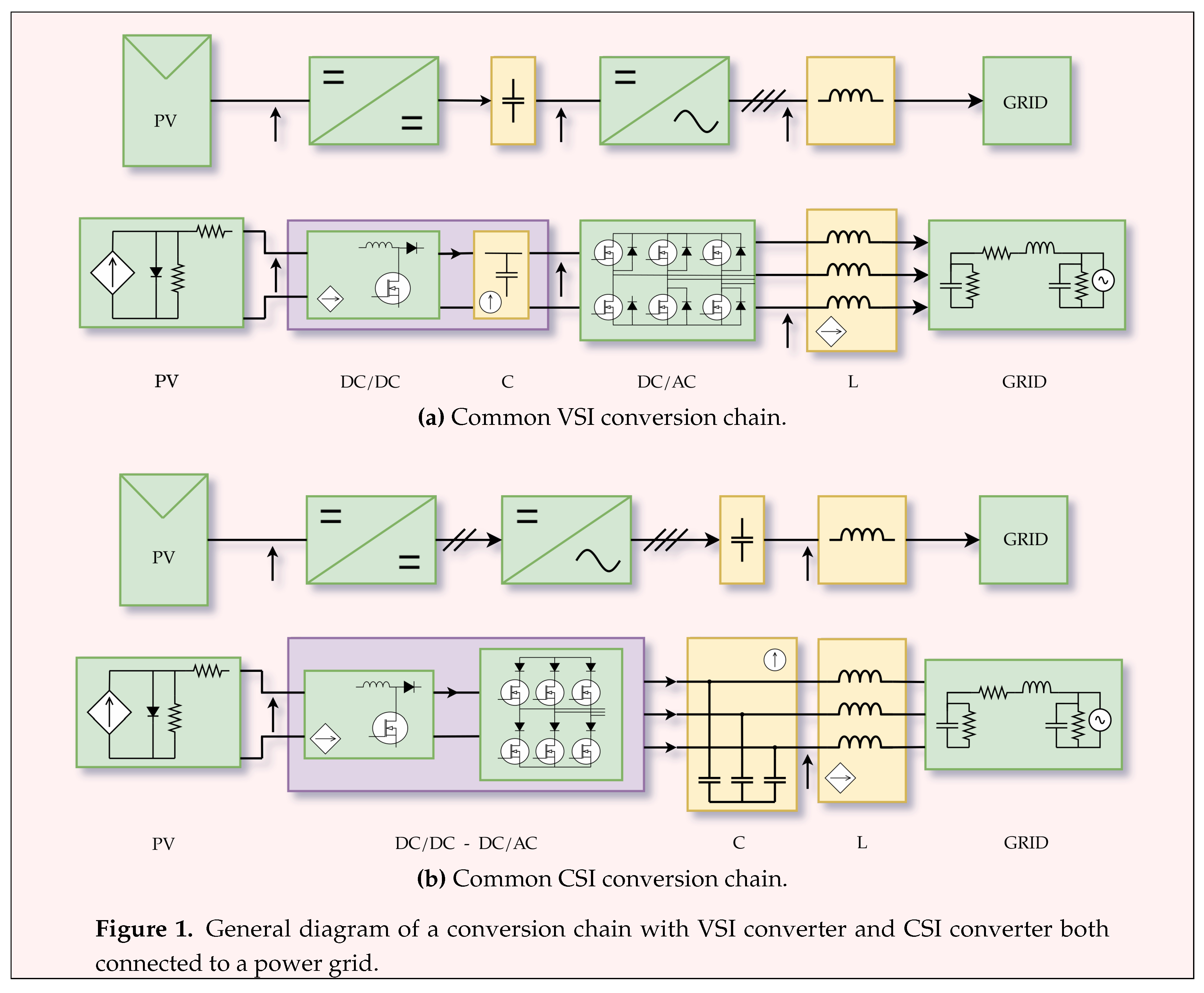
Figure 1 shows the most commonly adopted conversion lines based on VSI inverters, see
Figure 1 and CSI inverters
Figure 1, both designed to allow the controlled transfer of electrical energy from a low voltage photovoltaic source to a electric grid. For each conversion line, a simplified conceptual diagram has been drawn, with the respective functional explanatory diagram at the bottom, in order to highlight the functions performed by the individual conversion elements and their characteristic circuits.
An important issue of PV conversion systems concerns their stability. As is well known, the tendency to instability is related to the impedance of the electric grid and its articulation. This feature is taken into account through the stability index [
8,
9,
10], which is strictly dependent on the overall impedance present on the connection node. As a result, grid stability is particularly critical for weak grids, microgrids, or isolated grids. From a strictly electrotechnical point of view,
Figure 1a allows some important considerations to be made:
The first is the need to insert a highly inductive elements to connect the VSI inverter with the grid, given that both VSI bridge and the grid could be considered as voltage generators. This fact has consequences on the difficulty in designing a current control system with sufficient dynamic performance to guarantee the control of the stability of the grid voltage [
11], furthermore, in this section, it is often necessary to use a transformer to reach sufficiently high voltage levels, introducing further factors that can influence the control dynamics [
12];
the second remark concerns the DC/DC conversion section which must be completed by a capacitive reactive element so that the inverter can be powered by voltage. The presence of a capacitance of a sufficiently high value does not allow high dynamic performance to be obtained in the DC-Link voltage control, compromises the dynamic capability of the MPPT control [
13,
14], and introduces sub-synchronous resonances [
15]. The choice of this capacitive element is critical, as it must be made on the basis of a difficult compromise given that, on the one hand, low value of the capacity reduce the settling time during environmental disturbances and allow the performance of the MPPT to be improved, on the other the inverter current control requires strong stability of the DC-link voltage and therefore an high value of capacity. As a consequence of these conflicting needs the design of whole conversion line results particularly difficult to manage [
16].
Considering the CSI inverter-based conversion line shown in
Figure 1b, the following considerations can be made:
the first is that the CSI can be considered, from a strictly electrotechnical point of view, a current generator, as such, it presents two interesting characteristics which are the ability to have a more stiff control current compared to the VSI and therefore to require the presence of reactive elements of much more limited value on the connection to the grid, (C) and (L). This foster the design of control systems for the current fed into the grid;
the second is that the inverter requires a current power supply, so the DC/DC converter has no capacity (C), so it is clear that many of the problems related to the control of VSI-based conversion lines, which have been mentioned above, are greatly reduced in the case of CSI. Numerous comparative studies have been done by researchers on these two different types of conversion [
17,
18,
19,
20] from which interesting evaluations have emerged that suggest the convenience of adopting one or the other based on specific applications. In particular, as regards the solution shown in
Figure 1b, notable advantages have been highlighted in the implementation and design of the control of the current feding the grid, furthermore the stability of the DC-link and the performance of the MPPT are significantly improved. An obvious drawback is the higher losses due to the currents recirculating in the DC-link inductor and in the bridge. The capacity value is lower, even if the DC-link inductor is particularly bulky and requires very careful design to limit conduction losses. Similar to what happens for passive elements, switching losses are better in power devices, but conduction losses are worse.
the third consideration, perhaps the most relevant, is that the CSI inverter has natural boost characteristics and therefore, if the DC/DC converter is designed to support this characteristic, it is possible to avoid transformers and also to limit the size of the necessary reactive elements, both on the DC-link and on the grid connection.
Further observations can also be made on the reliability of the two systems, remembering that the CSI has an intrinsic short circuit capability, and shows greater general reliability. Based on all these considerations, the type chosen is the one based on the CSI converter, i.e. the one shown in
Figure 1b. On this conversion line it is now necessary to identify the types of the two DC/DC and DC/AC conversion stages and carry out a first rough sizing of the passive elements, keeping in mind that the sizing of the latter will have to be refined on the basis of the required dynamic performance of regulation systems.
3. CSI Bridge
In order to better introduce the common problem of the CSI topology and outline the solution, the CSI operation and the adopted modulation technique is reported below. The CSI bridge adopted in this project is based on a classic scheme, it is made up of three branches composed of power devices with diodes in series for blocking the currents during the switching phases .
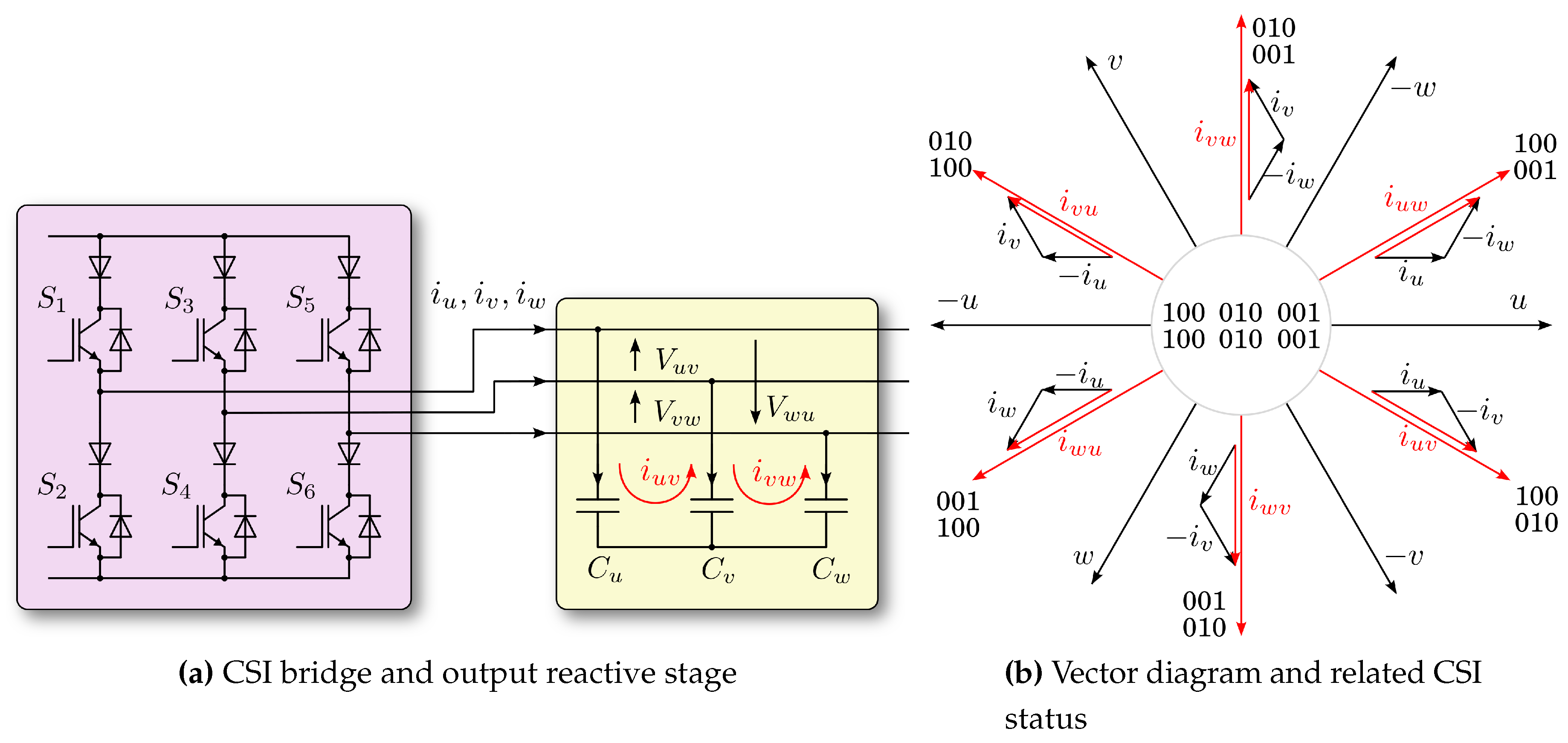
The generic scheme is the one shown in
Figure 2a.
Figure 2b is rather trivial and is common to all CSI bridges, it represents the current base vectors that can be generated depending on the states of the devices. At the center of the diagram are the three free-wheeling states that do not circulate current in the capacitor bank.
3.1. CSI Modulation Strategy
Less trivial, however, is the strategy that can be implemented to obtain a certain current value at the output of the bridge, or to pursue a certain voltage value, set as a reference. The scientific literature is full of more or less sophisticated solutions on this subject.
In the proposed implementation, the following criteria were followed to design the switching strategy for this project:
Reduce the complexity of the calculation algorithms given that the entire modulation and control system will have to be implemented on a single microcontroller (TI F28379D). Programming is performed using Simulink Embedded Coder® Support Package, which offer important advantages for rapid prototyping, software portability, and the production of standardized code for embedded systems. The Simulink models described below were programmed according to criteria for the automatic production of code on a microcontroller, therefore the functions for managing code under interrupt and the discretization of some variables were implemented;
Modulation with vector current references, therefore of SVM type;
Use of techniques aimed at the optimal exploitation of the devices, therefore symmetrical modulation in the respective quadrants.
Based on these indications, hereafter we can describe the various elements and the performed functions. Calling the reference current, it is broken down into its module and phase components , .
The entire time interval during which the first active state of the bridge is activated is calculated with the expression
, where
is the relative switching frequency with asymmetric modulation,
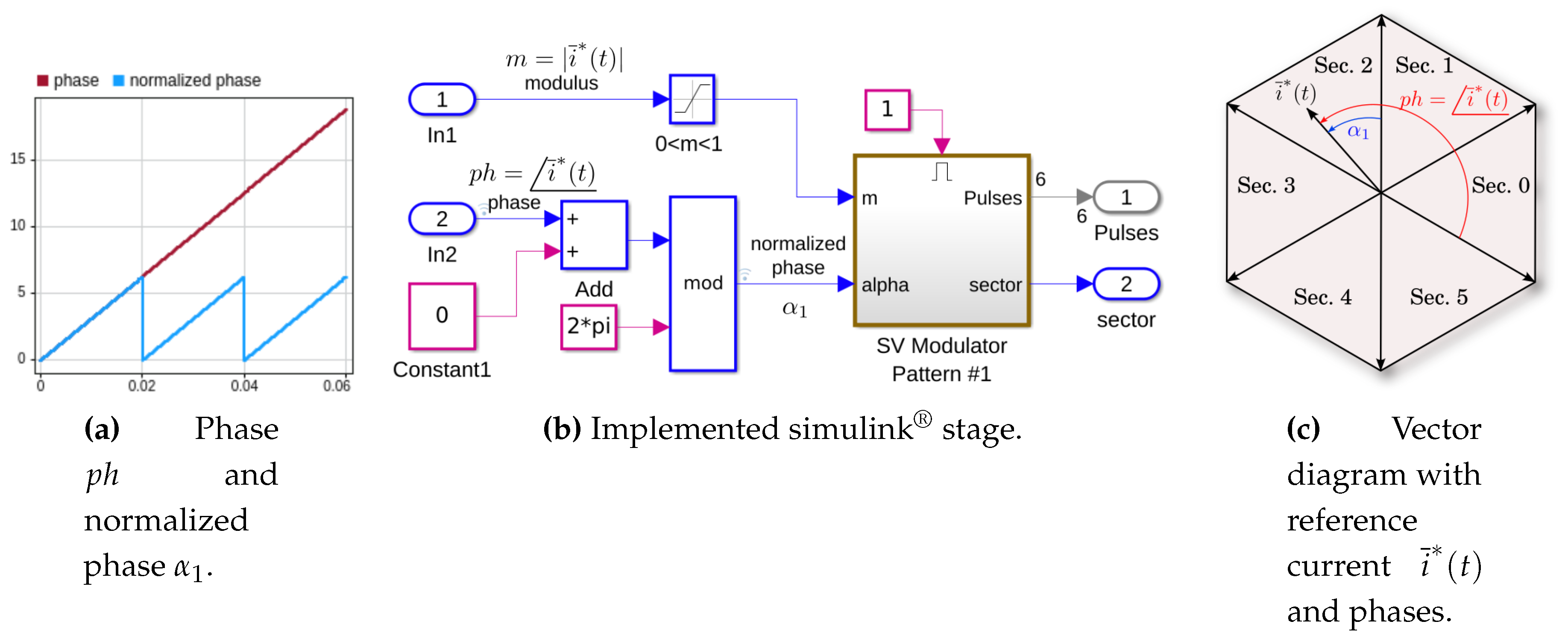
is the value of the reference current anomaly with respect to the first basis vector of the sector in which the reference current is located, see
Figure 3. The entire time interval during which the second active state of the bridge is activated is calculated with the expression
. The entire time interval during which the bridge must be in one of the states producing zero current on the three-phase system is given by the difference
.
The sector in which the reference current lies is obtained from the phase value, which is calculated with the aid of a look-up table which implements the function
. This type of implementation, see
Figure 4, was chosen to make the microcontroller code more efficient.
The subsequent functions transform
,
, and
into the corresponding time intervals. In particular,
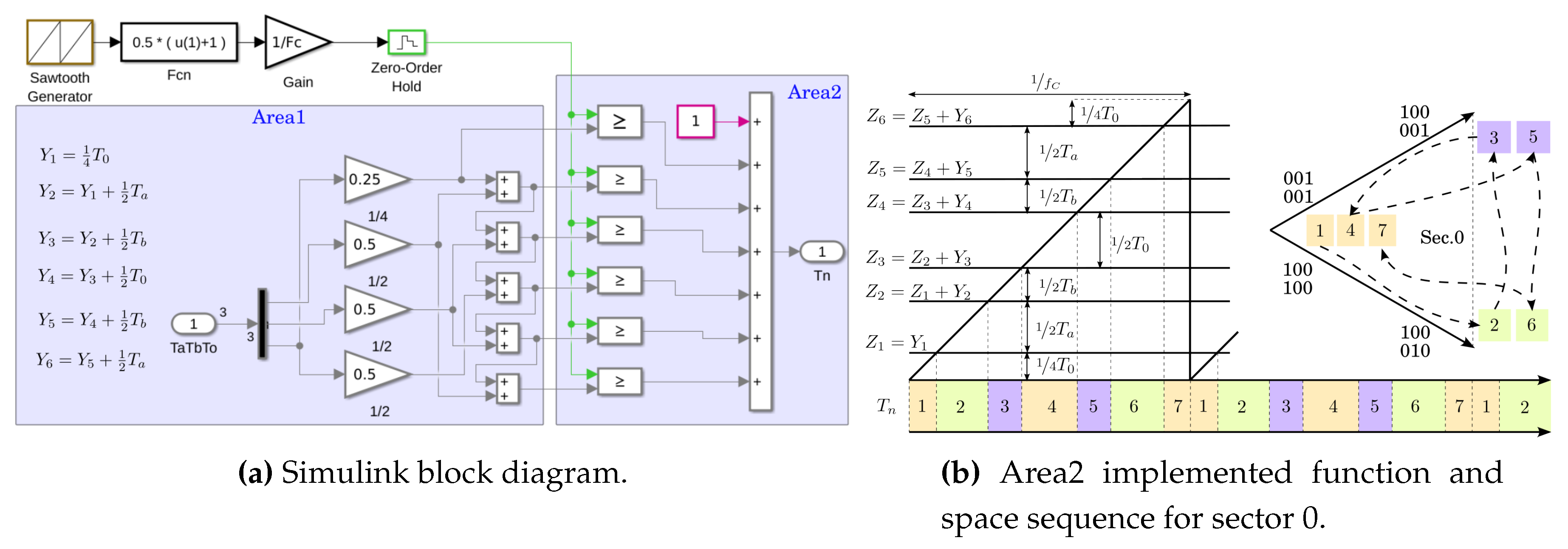
Figure 5 shows the code that calculates the sequences with which the states of the bridge follow one another in any of the sectors. In this case, although the ramp used to generate the time base has a sawtooth shape, the switching strategy is symmetrical, however, it is relatively easy to swap to asymmetric switching by modifying the code reported in Area1. The model reported in Area2 generates the
numbering.
Figure 5b shows the temporal diagram of the switching sequences and the spatial representation of the bridge states in sector 0 chosen as an example. The
numbering, together with the sector number, are the input variables for a 3D matrix in which the states of the six bridge devices
are stored. The device states are shown in the
Table A1 in the Appendix A.
3.2. Dead Time Implementation
Of course, there are numerous methods for implementing dead-times in a CSI bridge modulator. In this project, it was chosen to avoid the use of indexed tables or matrices, preferring a direct calculation technique also based on the measurement of the state of the bridge in real time.
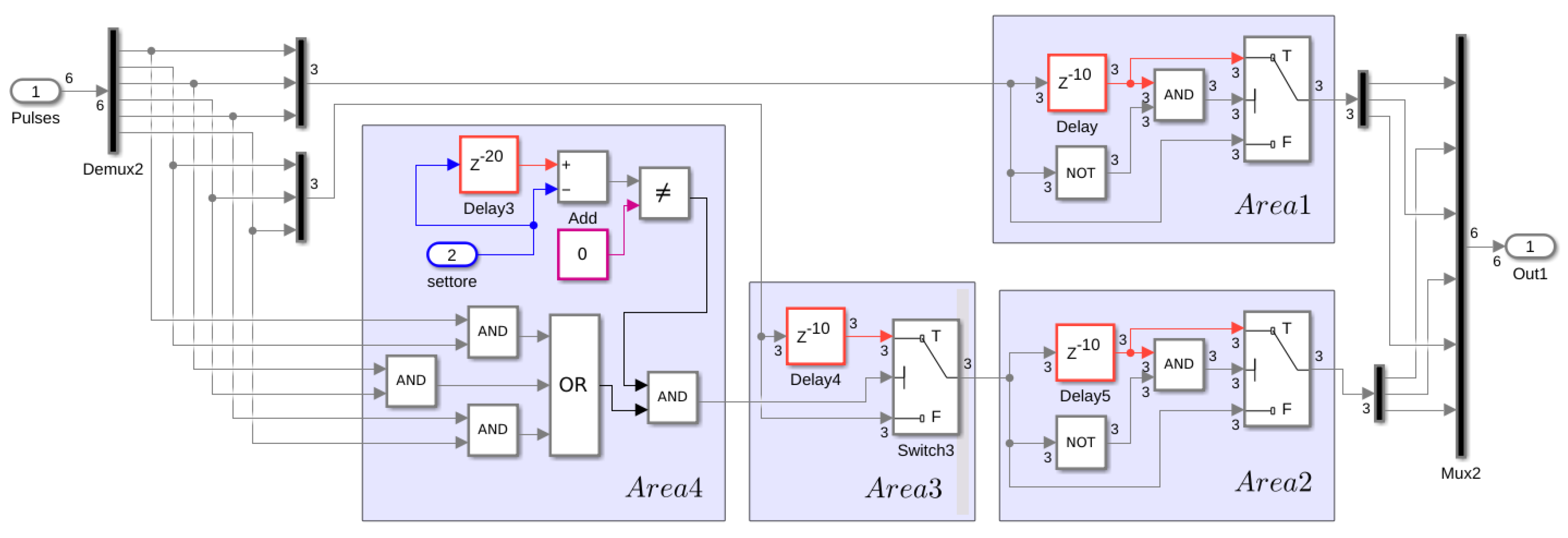
Referring to the diagram of
Figure 6, some areas have been highlighted in order to make the identification of functions clearer. The introduction of the dead time is done by delaying the falling edge of all six device control signals by an amount equal to
, where
is the smallest calculation period with which the microcontroller interrupt routines are managed . The delay is introduced by the sections indicated with
and
. The value of
is a project parameter and can depend on numerous factors, including the choice of the type of power devices. An exception has been introduced in this simple procedure which consists in delaying the control signals of devices
when there is a sector change and when the state of the devices is in current free-weeling. The detection of the free-wheeling state is carried out by the code of
, the further delay is introduced by the elements present in
. This correction, although introducing a small distortion in the current control, is necessary to avoid too short switching intervals near the transition between one sector and the adjacent one. Intervals of this type may not be adequately managed by the drivers and may have unpredictable consequences on the real state of the devices. It was therefore preferred to implement a more robust solution rather than a perfectly linear SVM modulation technique.
4. Key Considerations on the DC/DC Conversion Stage Structure and Control
On the basis of the foregoing, it is necessary to identify a conversion topology for the DC/DC - voltage/current stage, capable of supporting and delivering a sufficiently stable current considering the voltage present on the input terminals of the CSI bridge.
4.1. DC/DC Stage Topology Selection for Low Voltage PV Source
For simplicity, let’s assume, in this phase, that the converter is connected to an ideal power grid. The CSI converter naturally presents a DC/AC operation if observed from the load towards the DC-link, the voltage present on the latter is extremely variable and is governed by the three-phase voltage on the terminals connected to the grid and by the CSI switching state that occurs at a given moment. See
Figure 7
The value of this voltage can vary from zero when the bridge is in the current recirculation state, to the peak l-l value of the grid when the bridge switches in correspondence with one of the maximum l-l grid voltage. Also, depending on the variability of the load and any reactive currents, it may occur that the voltage control system on the grid node injects a current such as to discharge the voltage on the bank of capacitors connected to the grid node, when this occurs switching state of the CSI reports a negative voltage on the DC-link. For the choice of DC/DC stage type, most suitable for this project, the following general specifications were taken into consideration: no transformer, no interlived type, no mutual coupling between inductors and high step-up capacity. The choice fell on the typology known as “switched-inductors” [
21,
22,
23,
24,
25] which seems to meet all the requests mentioned.
4.2. General topology of proposed system and validation of DC/DC converter stage
In order to validate the choice some simulations in MATLAB-SIMULINK® were carried out.
The
Figure 8 shows the basic scheme on which the simulations were performed. The
Figure 8b represents the real scheme adopted in the simulation in which the CSI bridge, of
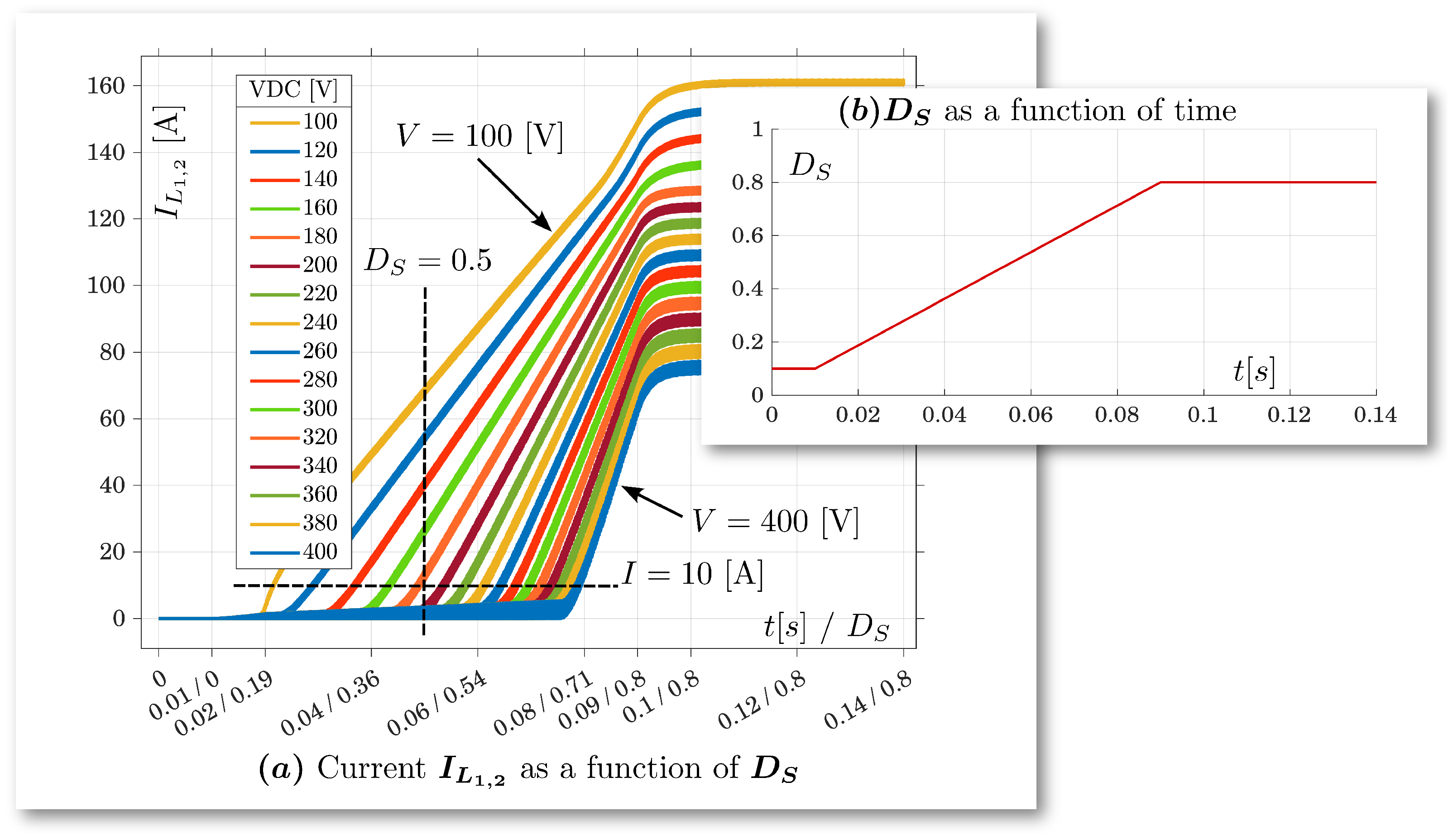
Figure 8a, was replaced by a variable voltage generator in order to reduce calculation times. This simplification does not affects the results we want to achieve since, in this case, we only want to characterize the DC/DC stage. The aim is to determine the ability of the "switched-inductors" to generate current both as a function of the Duty-Cycle, with which the S device is controlled, and as a function of the DC-link voltage set by the CSI bridge. The overall simulation consists of sixteen distinct simulations in which the VPV voltage is kept constant at a value of
, each of them was performed with different V
DC voltage values between
and
. The resulting data is shown in the
Figure 9. Each simulation is carried out for a total time interval of 140 [ms]. During this interval the Duty-Cycle, which we briefly indicate further down with the symbol
DS, is adjusted according to the curve shown in
Figure 4b. The curves in
Figure 4a show the current of inductors
IL1,2 and
IL2 that can be transferred from the DC/DC stage to the CSI according to the following expression
Where
represent the local mean value of current.
With these data the following considerations can be made:
Considering these data, the DC/DC stage based on switched inductors appears to be an excellent candidate to meet the specifications both for its ability to generate the required current, for its voltage boost capabilities and, last but not least, for its circuital simplicity.
It is worth observing that the curves in the
Figure 9 have completely general features and therefore represent a useful general characterization of the "switched-inductors" circuit.
4.3. Converter topology and lay-out issues
Modulation techniques for CSI converters are, and still are, studied extensively by the scientific community [
24,
26,
27,
28]. The main objectives of this research can be summarized in the following points:
reduction of the harmonic content of the voltage generated by the CSI;
reduction of switching losses;
improvement of dynamic performance;
improve the exploitation of switching devices and balance switching and conduction losses.
The main objectives of the choice of the modulation technique is the containment of the harmonic distorsion of current sipplied in the grid, and the optimization of the performance in terms of overall efficiency. This involves making suitable technological choices, such as the selection of power components, making the most of their performance, also by increasing the switching frequency, and adopting modulation techniques that allow the THD value to be reduced. As is known, one of the most significant drawbacks of the CSI converter, compared to the VSI, are the outstanding conduction losses. The designer can act on various fronts in order to mitigate these losses. The first is certainly to use devices that have a low R
ON value, another important design aspect concerns the choice of the topology of the conversion system and as a direct consequence the layout design which must also take into account the losses due to conduction of the tracks of the printed circuit and, as already mentioned, the reduction of parasitic inductances. The choice of switching devices will be discussed later in the text, here it is appropriate to describe the method used in selecting the circuit topology. Many CSI configurations, especially those dedicated to conversion systems for photovoltaic systems, adopt the so-called fourth leg which supports the three legs of the bridge. This additional electrical branch was introduced to reduce common mode variations and earth leakage current [
29,
30] and also with the purpose of recirculating the free-wheeling current along a path with a single power device instead of through two devices of any one of the bridge branches [
31]. This solution, although effective in some cases, seems to be less suitable for photovoltaic applications as it requires the use of additional reactive elements to prevent the recirculating current from passing through the photovoltaic modules. A different circuit configuration solution, quite simple and widely described by [
22,
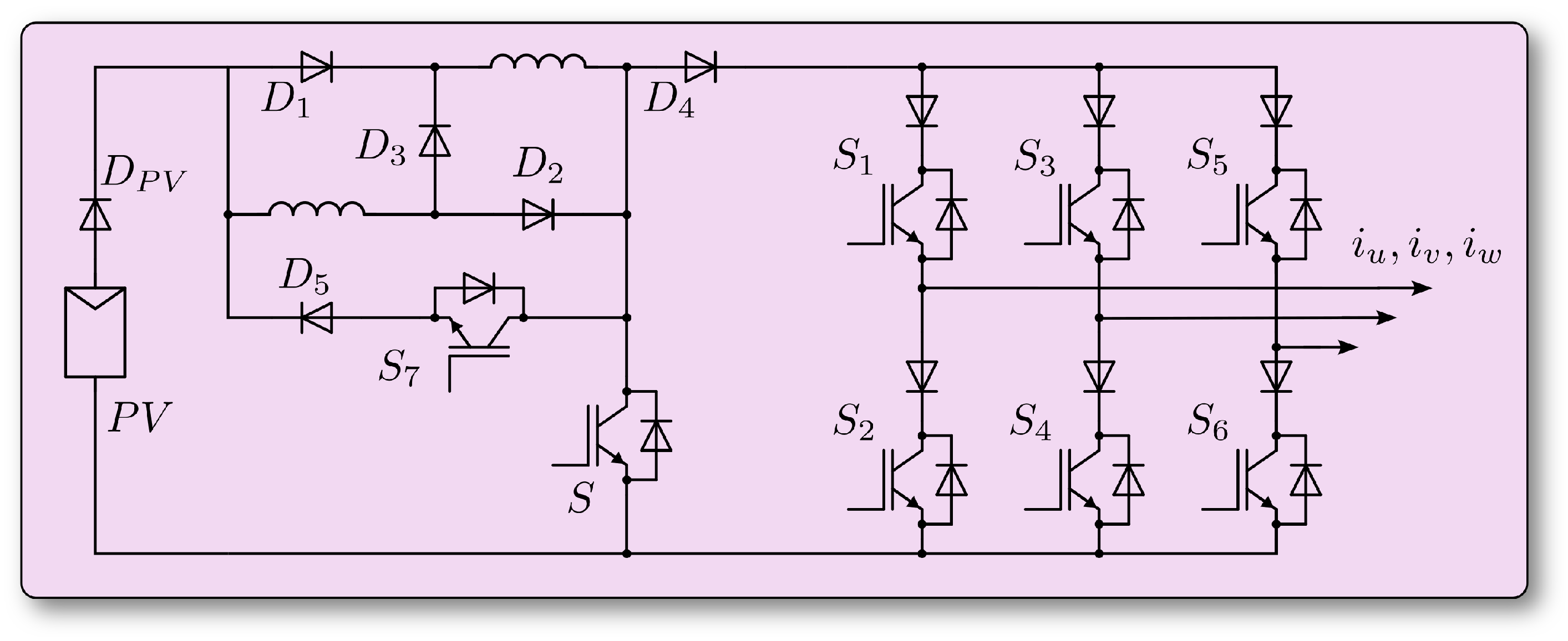
23], involves the recirculation of the current exactly at the ends terminals of the switchg-inductors as shown in
Figure 10 through the S7 device which must be activated during free-wheeling intervals. This solution also has another important advantage because it allows to design a printed circuit characterized by minimum paths of the recirculation current. It is also worth remembering that switching a current in a CSI inverter, unlike what happens in a VSI inverter, also implies a serious commitment in studying the layout of the converter: it is particularly important to reduce parasitic inductances to the minimum possible present in electrical meshes in which strong current variations are present. Otherwise, such current switching generates strong voltage variations which can compromise the integrity of the components and produce serious electromagnetic compatibility and susceptibility problems.
4.4. Compatibility of a Single DC/DC Boost Stage with the CSI Bridge
As extensively described in [
21,
22,
23,
24,
25] the switched-inductors circuit allows the charging of the inductors in parallel when the device S of
Figure 10 is in the ON state, and allows the discharge of the accumulated current of the series inductors when the device S is in the OFF state. The voltage at the input terminals of the CSI bridge can overlap with the states of the device S and consequently modify the charging and discharging state of the switched inductors. For example, this happens when switch S is in the ON state and the
voltage is negative. In this case the current flows through the bridge rather than through the device S. Similarly, but electrically symmetrical way, it is not possible to transfer current from the boost modules to the bridge when the
voltage is greater than the voltage across the
series inductors. As can be seen from the paragraph
4.2, in which the characteristics of the “SI” circuit have been reported, these circumstances cannot be avoided because the correct functioning of the DC/DC stage requires that the device S must be controlled with a Duty-Cycle adjusted up to at least a value of 0.8. At this point we must note that the two conversion stages, the CSI bridge and the DC/DC boost, cannot be considered as independent entities. The respective regulation systems have as their primary objective, the first, i.e. the one of the bridge, the regulation of the voltage on the grid node, and the second, i.e. that one of the "SI" module, the regulation of the current on the DC-link. The regulation system that controls the module and the phase of the SVM modulator is relatively simple if the DC-link current is assumed to be constant or in any case variable in a limited range. However, it would be advisable for the current available at the DC-link to be of a value commensurate with the current requested by the load. The control system of the DC/DC boost stage requires the adjustment of the duration of the time intervals during which to charge the current inductors and transfer this current to the bridge, however, as already mentioned, these phases are subject to the value of the DC-link voltage and then to the status of the bridge devices. In short, the two conversion stages are not independent either by electrical point of view or by a logical point of view. This fact suggests two different design paths: The first involves the study and implementation of a sophisticated control system that takes into account the interactions between the two converters and is able to guarantee the voltage profile on the grid node in the case of an isolated grid, or the current requested by the load in the case of a prevailing power electricity grid, and also the optimal management of energy flows and, consequently, the best performance of the system. The second way is to look for a HW solution that makes the two systems independent. In this way, the relevant controls can be significantly simplified by managing both the energy flow on the grid node and the current on the DC-Link in a simpler way. In this project the second path was followed.
4.4.1. Doubling Switched-Inductors
One proposal to provide independence to the two stages is to introduce a further module with switched inductors, in parallel to the first. The two modules can be controlled alternatively, i.e. while one of them can discharge the current to the bridge, the other can be in the charging phase.
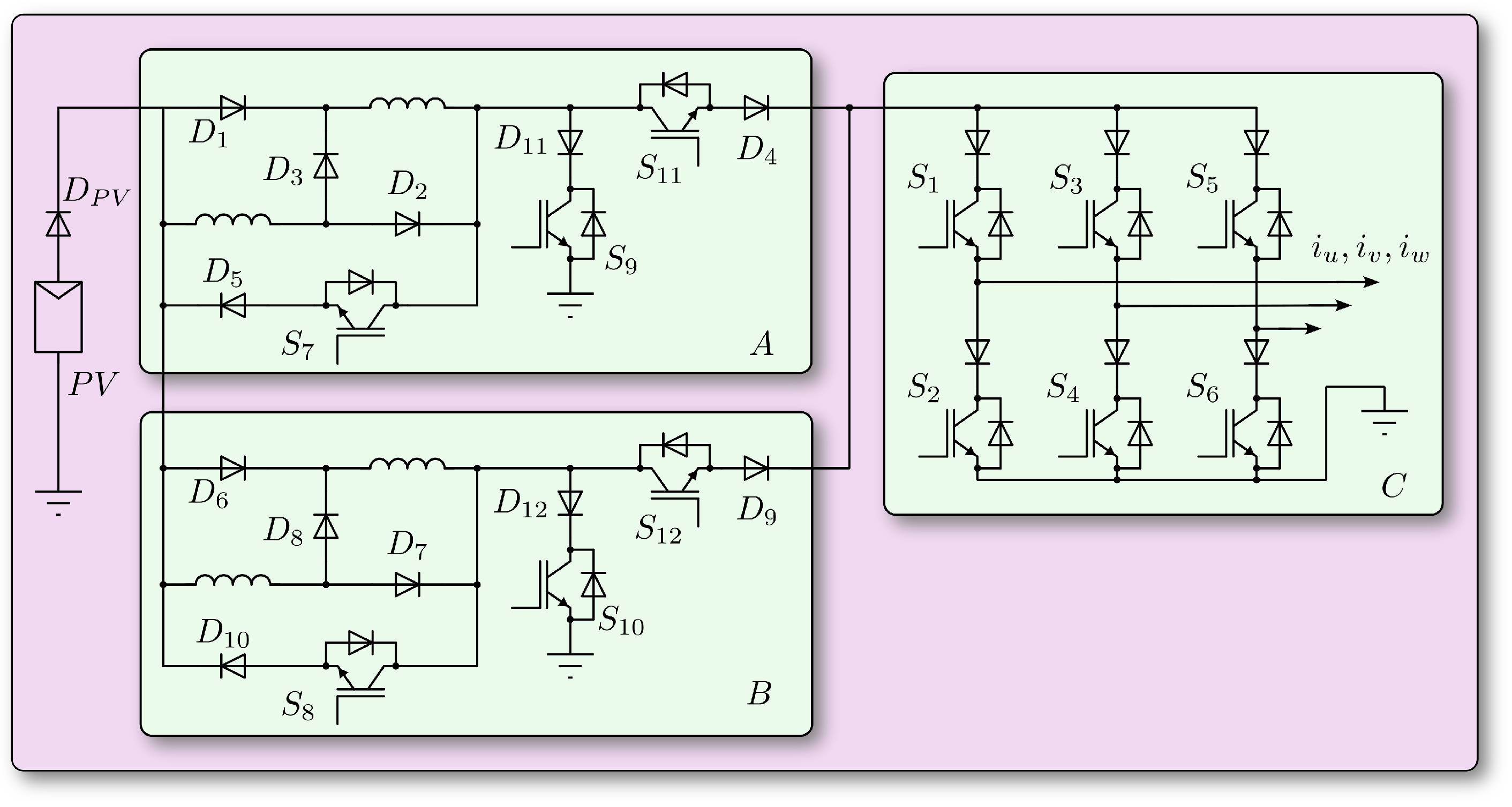
The difficulty of coordinating the states of the boost module with the states of the bridge suggests introducing a further module with switched inductors, in parallel to the first. In this configuration, shown in
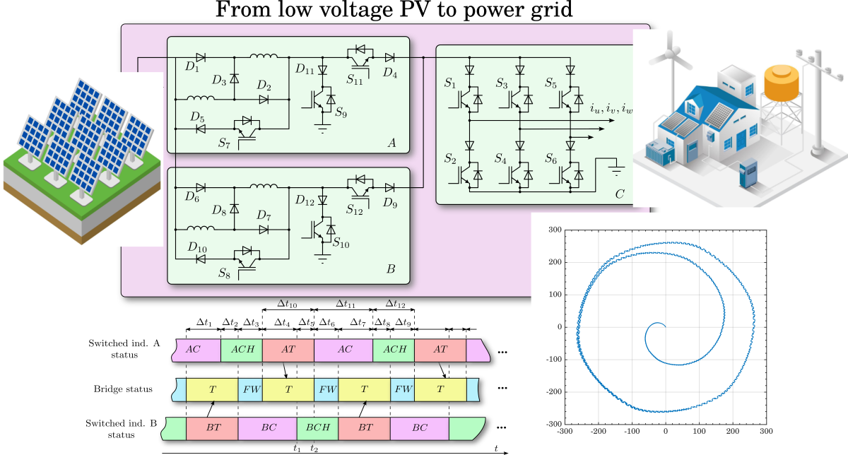
Figure 11, the two modules can be controlled in an alternative way. The coordination of the states of the two SI modules with respect to the states of the bridge is shown in
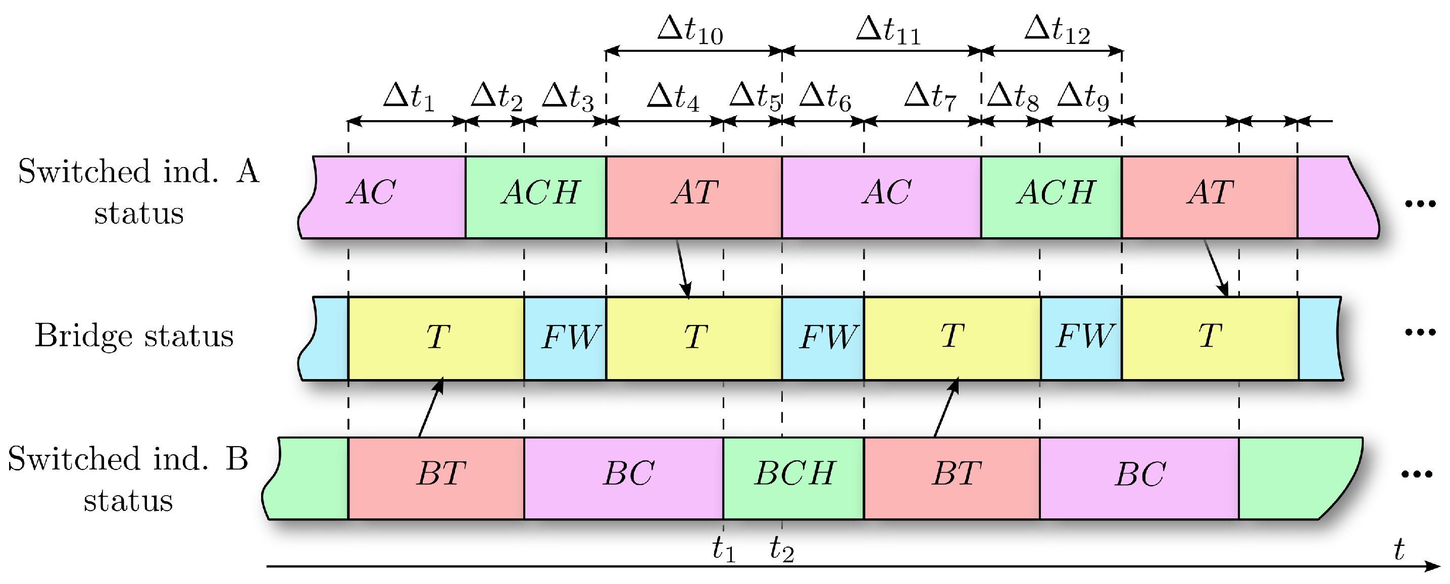
Figure 12, in which three bands are drawn that develop as a function of time. The central one represents the states of the bridge, it considers the "passive" free-wheeling state, indicated with FW and the "active" state when the current is transferred to the grid, indicated with T. The other two bands respectively represent the status of the SI-A module and those of the SI-B module. Each of these modules can be in one of the following three states: “charging”, indicated by AC in the case of module A, “transfer” indicated by AT and “current holding”, indicated by ACH . The time intervals in which there is current transfer towards the bridge and from the bridge to the grid node (AT and T), must coincide in an alternative sequence, i.e. the current flow must be guaranteed alternatively by the SI modules, as indicated by the arrows. The complementary time interval, for each of the SI modules, respectively AC+AFW and BC-BFW, can be managed to regulate the duty cycle of each of the modules and therefore the current accumulated by them. There is the possibility of an overlap of the AC and BC states, in this case it is necessary to verify the electrical compatibility of this event with the photovoltaic power system. In case of incompatibility, the constraint
must be introduced in the control logic. The overall scheme is certainly more complex, the number of power devices increases considerably, as do the drivers necessary to control their state, however regulation variables are introduced which allow simpler and more precise control of both the DC current and the voltage (or current) towards the grid node.
Table 2 reports the status of the power devices together with the status of bridge. It allows us to better explain the sequence of events and states in the intervals that follow one another over time.
5. Simulation Results
Below are some results obtained through simulation of the SIMULINK® model of the system useful for characterizing and defining the general performance in steady state. In the simulation, an isolated grid was connected on which there is a load of []. The capacitor bank on the same grid node consists of a star with a capacitance equal to [50 ]. The reference values of the magnitude of the space vector generated by the CSI modulator and the Duty-Cycle of the CSI converter have been set. In these conditions, slight distortions of the voltages present on the grid node will be visible. This is due to the absence of regulation of both the module and phase of the grid voltage, and of the DC-link current module.
The simulation data spans 60[ms]. The voltage of the photovoltaic system is generated via an increasing ramp starting from 5[ms] and ending with 80[V] at 80[ms]. The magnitude of the current vector generated by the CSI modulator is set at 45%. The states of the SI modules are equal to each other and extend for a total of 164 us. Each time interval, as also reported in
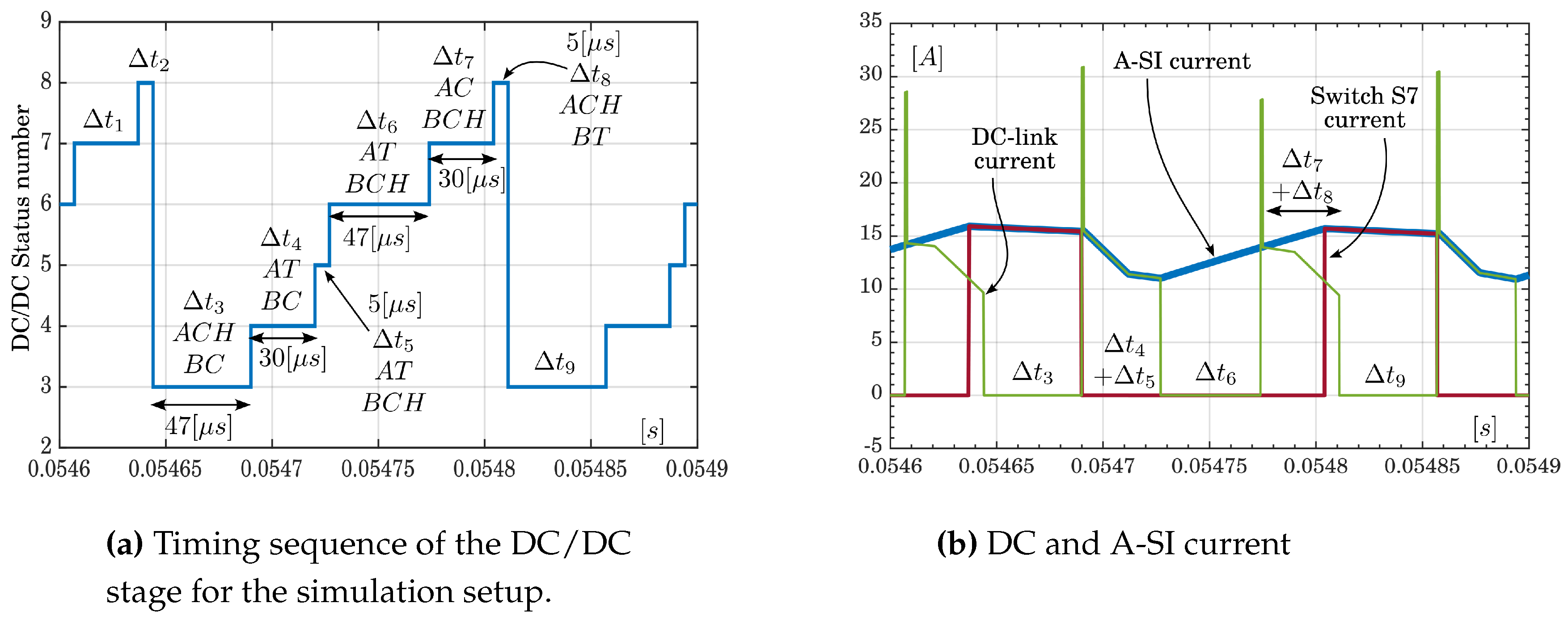
Figure 12, has been fixed and the timing is reported in
Figure 13a:
Figure 13b shows the current diagram of the DC-link, the current diagram in one of the inductors L of the A-SI module and the current in the S7 device. The time interval is the same as in
Figure 13a:
.
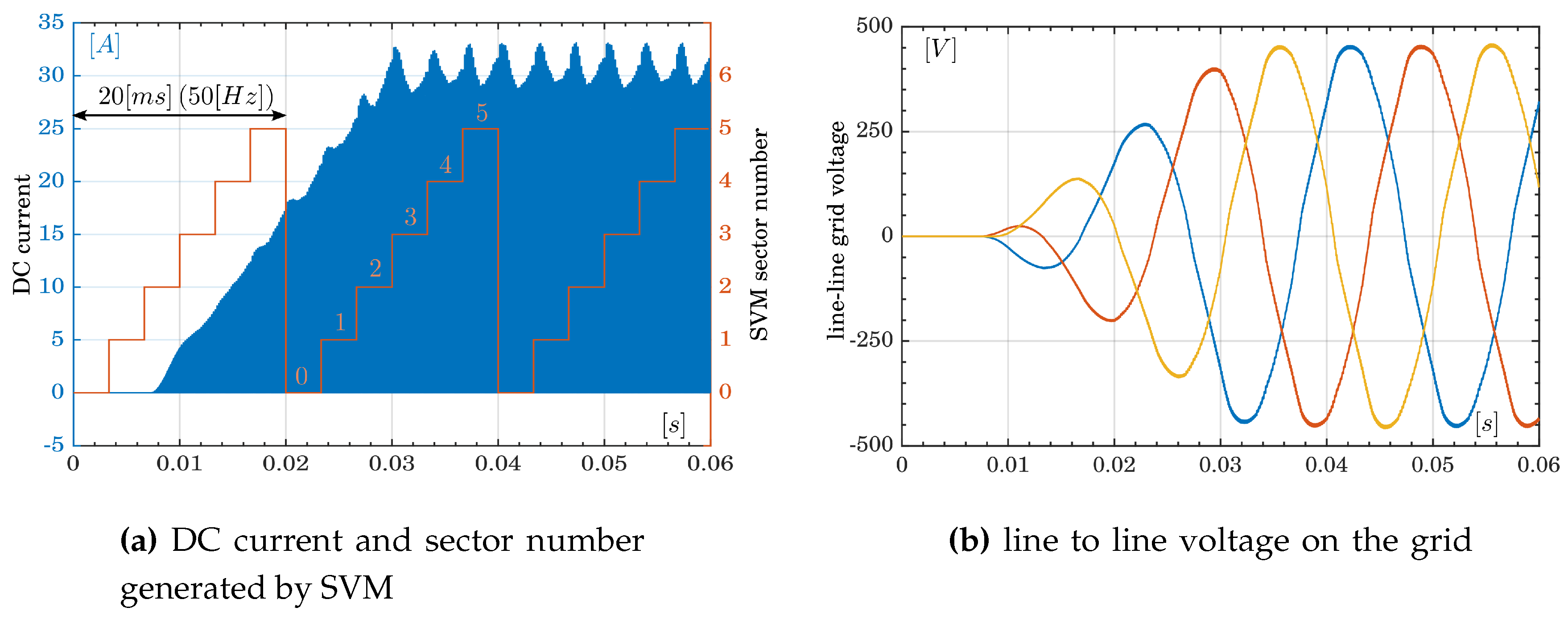
Figure 14a reports the DC-link current for the entire similation period
and, as a temporal and spatial reference, a diagram representing the number of SVM sector. On the right side the line-to-line voltages of the grid are shown, which, in this case, is assumed to be of the isolated type. The power transferred to the load is
.
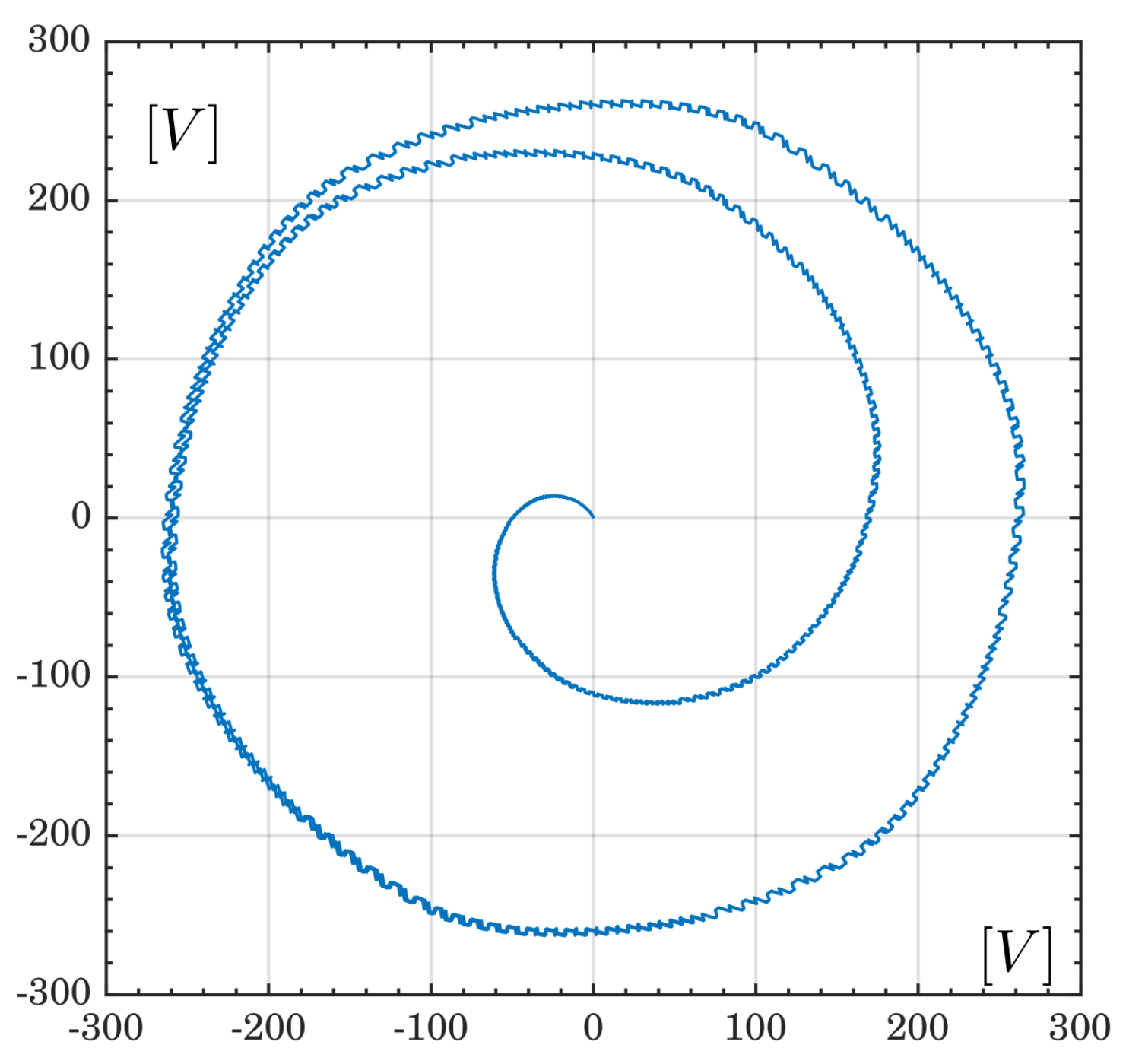
Figure 15 shows the path of the voltage space vector to the grid node.
6. Discussion
This paper dealt with the design procedure, leading to the definition of a conversion topology that allows to transfer the energy from a low voltage photovoltaic system to a three-phase electrical grid with a nominal voltage of both of isolated type and of prevailing power. The target power is . In this context the dynamic performances of the entire conversion system will not be reported, because these will be dealt with in a future manuscript where all the control functions will be described in detail. The specifications for the construction of this conversion system were dictated by industrial and commercial needs. The requirement to make a large voltage step has, in general, significant negative implications on the performance of the entire system, however the design choices made have sought to limit energy dissipation as much as possible. From this need, a synchronized modulation strategy between the states of the bridge and the states of the SI modules has been identified. It is worth noting the following points considered peculiar by the authors:
The topolgy identified and the modulation technique described allow an independent regulation of the DC-link current and of the current that the bridge transfers to the grid. In the case of a distributed grid, these choices favor the design of a dynamically more efficient system for the regulation of the power absorbed by the photovoltaic system and therefore to implement more performing MPPT strategies. In the case of an isolated grid, the punctual management of the current allows to respond more quickly to the requests of the connected load, limiting to a minimum the circulation of current inside the conversion system and reducing the conduction losses both in the inductors and in the power devices.
The data represented in
Figure 9, together with the description of the method with which they were obtained, are useful for the characterization of a cascaded SI module with a generic voltage generator in the range of the electrical quantities that were used, therefore they are general data useful for the design of systems that adopt this conversion topology.
The possibility of recirculating the current through the inductors of the DC/DC stage allows to avoid the use of the so-called fourth leg of the CSI bridge, known in literature with the acronym CSI7 or H7 [
30,
32,
33], since the current coming from the SI modules is zero during the free-wheeling of the bridge, despite this typology being established with a certain frequency in the design of CSI converters and has even been defined as a "universal solution for CSI converters" [
31].
With the aim of improving the losses due to the switching and conduction of the devices, SiC type components were adopted which present significantly superior performance in terms of voltage drop in ON-state [
34,
35,
36] and particular attention was paid designing switched inductors.
7. Patents
Patent Pending: Application IT102024000019174
Author Contributions
Conceptualization, R.D.; methodology, R.D.; software, R.D.; validation, R.D. and F.M.; formal analysis, R.D. and F.M.; investigation, R.D. and F.M.; resources, R.D. and F.M.; data curation, R.D. and F.M.; writing—original draft preparation, R.D.; writing—review and editing, R.D and F.M.; visualization, R.D, F.M. and F.P.; supervision, R.D and F.M.; project administration, R.D, F.M. and F.P.; funding acquisition, R.D and F.P.; All authors have read and agreed to the published version of the manuscript.
Funding
This research was funded by Cloudwise s.r.l.
Acknowledgments
The authors thankfully acknowledge Industrial Electronics Laboratory of University of Cassino “G. D’Angelo” for technical advice and support. The authors also thankfully acknowledge to the anonymous reviewers whose comments have helped us to enhance our work.
Conflicts of Interest
The authors declare no conflicts of interest.
Abbreviations
The following abbreviations are used in this manuscript:
| CSI |
Current Source Inverter |
| SI |
Generic switching Inductors module |
| VDC
|
DC-link voltage |
| S |
generic switch device of DC/DC boost stage |
| DS |
Duty-Cycle of one stage DC/DC |
| IL |
Inductor current |
| SVM |
Space Vector Modulation, or Space Vector Modulator |
|
local mean value of DC-link current |
| T |
Transfer mode of CSI bridge |
| FW |
Free Wheeling mode of CSI bridge |
| A-SI |
Switching inductors module A |
| B-SI |
Switching inductors module B |
| AC |
A-SI Charging state |
| ACH |
A-SI Current Holding state |
| AT |
A-SI current Transfer state |
| BC / BCH / BT |
The same as above but for the B-SI module |
Appendix A
Appendix A.1. 3D data table containing the switching status
The following table reports the data of the switching status which are referred in
Table A1.
Switch matrix implemented in the SVM.
Table A1.
Switch matrix implemented in the SVM.
| device |
|
|
|
|
|
|
|
|
|
|
|
|
| 1 2 3 4 5 6 7 |
1 2 3 4 5 6 7 |
1 2 3 4 5 6 7 |
1 2 3 4 5 6 7 |
1 2 3 4 5 6 7 |
1 2 3 4 5 6 7 |
|
1 1 1 0 1 1 1 |
0 1 0 0 0 1 0 |
0 0 0 1 0 0 0 |
1 0 0 0 0 0 1 |
0 0 0 0 0 0 0 |
0 0 1 1 1 0 0 |
|
1 0 0 0 0 0 1 |
0 0 0 0 0 0 0 |
0 0 1 1 1 0 0 |
1 1 1 0 1 1 1 |
0 1 0 0 0 1 0 |
0 0 0 1 0 0 0 |
|
0 0 0 0 0 0 0 |
0 0 1 1 1 0 0 |
1 1 1 0 1 1 1 |
0 1 0 0 0 1 0 |
0 0 0 1 0 0 0 |
1 0 0 0 0 0 1 |
|
0 1 0 0 0 1 0 |
0 0 0 1 0 0 0 |
1 0 0 0 0 0 1 |
0 0 0 0 0 0 0 |
0 0 1 1 1 0 0 |
1 1 1 0 1 1 1 |
|
0 0 0 1 0 0 0 |
1 0 0 0 0 0 1 |
0 0 0 0 0 0 0 |
0 0 1 1 1 0 0 |
1 1 1 0 1 1 1 |
0 1 0 0 0 1 0 |
|
0 0 1 1 1 0 0 |
1 1 1 0 1 1 1 |
0 1 0 0 0 1 0 |
0 0 0 1 0 0 0 |
1 0 0 0 0 0 1 |
0 0 0 0 0 0 0 |
References
- UN. The Sustainable Development Agenda. https://www.un.org/sustainabledevelopment/.
- Semenova, N.; Hassel, L.G. On the Validity of Environmental Performance Metrics. Journal of Business Ethics 2014, 132, 249–258. [Google Scholar] [CrossRef]
- Escrig-Olmedo, E.; Fernández-Izquierdo, M.; Ferrero-Ferrero, I.; Rivera-Lirio, J.; Muñoz-Torres, M. Rating the Raters: Evaluating how ESG Rating Agencies Integrate Sustainability Principles. Sustainability 2019, 11, 915. [Google Scholar] [CrossRef]
- Braccini, A.; Margherita, E. Exploring Organizational Sustainability of Industry 4.0 under the Triple Bottom Line: The Case of a Manufacturing Company. Sustainability 2018, 11, 36. [Google Scholar] [CrossRef]
- Wang, X.; Blaabjerg, F. Harmonic Stability in Power Electronic-Based Power Systems: Concept, Modeling, and Analysis. IEEE Transactions on Smart Grid 2019, 10, 2858–2870. [Google Scholar] [CrossRef]
- Enslin, J.; Heskes, P. Harmonic Interaction Between a Large Number of Distributed Power Inverters and the Distribution Network. IEEE Transactions on Power Electronics 2004, 19, 1586–1593. [Google Scholar] [CrossRef]
- Li, Y.; Fan, L.; Miao, Z. Wind in Weak Grids: Low-Frequency Oscillations, Subsynchronous Oscillations, and Torsional Interactions. IEEE Transactions on Power Systems 2020, 35, 109–118. [Google Scholar] [CrossRef]
- Ali, K.; Putranto, L.M.; Imam, A.; Tumiran.; Yasirroni, M. Determination of Optimal PV Energy Share Considering Voltage Stability Index. In Proceedings of the 2020 2nd International Conference on Smart Power amp; Internet Energy Systems (SPIES). IEEE, 2020. [CrossRef]
- Uzun, U.E.; Pamuk, N.; Taskin, S. Effect of Solar Photovoltaic Generation Systems on Voltage Stability. In Proceedings of the 2022 Global Energy Conference (GEC). IEEE; 2022. [Google Scholar] [CrossRef]
- Sun, J. Impedance-Based Stability Criterion for Grid-Connected Inverters. IEEE Transactions on Power Electronics 2011, 26, 3075–3078. [Google Scholar] [CrossRef]
- Holmes, D.G.; Lipo, T.A.; McGrath, B.P.; Kong, W.Y. Optimized Design of Stationary Frame Three Phase AC Current Regulators. IEEE Transactions on Power Electronics 2009, 24, 2417–2426. [Google Scholar] [CrossRef]
- Midtsund, T.; Suul, J.A.; Undeland, T. Evaluation of current controller performance and stability for voltage source converters connected to a weak grid. In Proceedings of the The 2nd International Symposium on Power Electronics for Distributed Generation Systems. IEEE; 2010. [Google Scholar] [CrossRef]
- Nasiri, M.; Chandra, S.; Taherkhani, M.; McCormack, S.J. Impact of Input Capacitors in Boost Converters on Stability and Maximum Power Point Tracking in PV systems. In Proceedings of the 2021 IEEE 48th Photovoltaic Specialists Conference (PVSC). IEEE; 2021. [Google Scholar] [CrossRef]
- Santra, S.B.; Chatterjee, D.; Kumar, K.; Bertoluzzo, M.; Sangwongwanich, A.; Blaabjerg, F. Capacitor Selection Method in PV Interfaced Converter Suitable for Maximum Power Point Tracking. IEEE Journal of Emerging and Selected Topics in Power Electronics 2021, 9, 2136–2146. [Google Scholar] [CrossRef]
- Moradi-Shahrbabak, Z.; Bakhshai, A.; Tabesh, A. Effect of dc-link capacitor on small signal stability of grid connected PV power plants. In Proceedings of the 2018 IEEE 12th International Conference on Compatibility, Power Electronics and Power Engineering (CPE-POWERENG 2018). IEEE, 2018. [CrossRef]
- Yan, G.; Ren, J.; Mu, G.; Jin, L.; Duan, S.; Jia, Q. DC-link voltage stability analysis for single-stage photovoltaic VSIs connected to weak grid. In Proceedings of the 2016 IEEE 8th International Power Electronics and Motion Control Conference (IPEMC-ECCE Asia). IEEE; 2016. [Google Scholar] [CrossRef]
- Azmi, S.; Ahmed, K.; Finney, S.; Williams, B. Comparative analysis between voltage and current source inverters in grid-connected application. In Proceedings of the IET Conference on Renewable Power Generation (RPG 2011). IET, 2011. [CrossRef]
- Potdukhe, K.C.; Munshi, A.P.; Munshi, A.A. Reliability prediction of new improved current source inverter (CSI) topology for transformer-less grid connected solar system. In Proceedings of the 2015 IEEE Power, Communication and Information Technology Conference (PCITC), Oct 2015, pp. 373–378. [CrossRef]
- Rajeev, M.; Agarwal, V. Single Phase Current Source Inverter With Multiloop Control for Transformerless Grid–PV Interface. IEEE Transactions on Industry Applications 2018, 54, 2416–2424. [Google Scholar] [CrossRef]
- Wang, Z.; Miao, Z.; Fan, L.; Yazdani, A. Weak Grid Operation of A Grid-Following Current-Sourced PV Solar System. In Proceedings of the 2021 North American Power Symposium (NAPS), Nov 2021, pp. 01–06. [CrossRef]
- Cheng, L.; Chen, P.; Yang, A.; Zhang, Q.; Wang, L.; Qian, Z.; Zhang, M.; Zhang, T. A Multilevel Asymmetric Current Source Inverter Topology Using Switched Inductor. In Proceedings of the 2022 4th International Conference on Power and Energy Technology (ICPET). IEEE; 2022. [Google Scholar] [CrossRef]
- Mao, M.; Zheng, Y.; Chang, L.; Xu, H. A single-stage high gain current source inverter for grid-connected photovoltaic system. In Proceedings of the 2015 9th International Conference on Power Electronics and ECCE Asia (ICPE-ECCE Asia), June 2015, pp. 1902–1907. Switched inductors, simulazione in matlab, PV. High voltage gain. Grid connected converter. Buona l’introduzione, utile per spunti: 3 state CSI. [CrossRef]
- Mao, M.; Li, Y.; Chang, L. Optimal design and experiment validation of switching inductor based tri-state CSI. In Proceedings of the 2017 Chinese Automation Congress (CAC), Oct 2017, pp. 6923–6927. [CrossRef]
- Li, C.; Chang, L.; Mao, M. Improved SVM for High Gain Tri-state CSI to Reduce DC Side Inductor Current Ripple. In Proceedings of the 2019 10th International Conference on Power Electronics and ECCE Asia (ICPE 2019 - ECCE Asia). IEEE; 2019. [Google Scholar] [CrossRef]
- Stephen, A.; K. P., R.; S, G. Review on Non-isolated High Gain DC-DC Converters. In Proceedings of the 2022 Third International Conference on Intelligent Computing Instrumentation and Control Technologies (ICICICT). IEEE, 2022. [CrossRef]
- Gnanasambandam, K.; Rathore, A.K.; Edpuganti, A.; Srinivasan, D. A Novel Optimal Space Vector Modulation Technique of Current Source Inverter for Solar Power Integration. In Proceedings of the 2018 IEEE International Conference on Power Electronics, Drives and Energy Systems (PEDES). IEEE, 2018. [CrossRef]
- Liu, Y.; Wang, M.; Xu, Z.; Yan, S. MPC Control of Three-Phase CSI in Unbalanced Grid. In Proceedings of the 2022 International Conference on Power Energy Systems and Applications (ICoPESA); 2022; pp. 357–361. [Google Scholar] [CrossRef]
- Aguirre, M.P.; Calvino, L.; Valla, M.I. Multilevel Current-Source Inverter With FPGA Control. IEEE Transactions on Industrial Electronics 2013, 60, 3–10. [Google Scholar] [CrossRef]
- Guo, X.; Xu, D.; Wu, B. Four-Leg Current-Source Inverter With a New Space Vector Modulation for Common-Mode Voltage Suppression. IEEE Transactions on Industrial Electronics 2015, 62, 6003–6007. [Google Scholar] [CrossRef]
- Anand, S.; Gundlapalli, S.K.; Fernandes, B.G. Transformer-Less Grid Feeding Current Source Inverter for Solar Photovoltaic System. IEEE Transactions on Industrial Electronics 2014, 61, 5334–5344. [Google Scholar] [CrossRef]
- Wang, W.; Gao, F.; Rui, S. Operation and modulation of H7 current source inverter with hybrid SiC and Si semiconductor switches. In Proceedings of the 2015 9th International Conference on Power Electronics and ECCE Asia (ICPE-ECCE Asia). IEEE; 2015. [Google Scholar] [CrossRef]
- Lorenzani, E.; Immovilli, F.; Migliazza, G.; Frigieri, M.; Bianchini, C.; Davoli, M. CSI7: A Modified Three-Phase Current-Source Inverter for Modular Photovoltaic Applications. IEEE Transactions on Industrial Electronics 2017, 64, 5449–5459. [Google Scholar] [CrossRef]
- Bendre, A.; Wallace, I.; Nord, J.; Venkataramanan, G. A current source PWM inverter with actively commutated SCRs. IEEE Transactions on Power Electronics 2002, 17, 461–468. [Google Scholar] [CrossRef]
- Catellani, S.; Bier, A.; Martin, J.; Gabriel, L.; Barruel, F. Characterization of 1.2kV Silicon Carbide (SiC) semiconductors in hard switching mode for three-phase Current Source Inverter (CSI) prototyping in. In Proceedings of the Proceedings of PCIM Europe 2015; International Exhibition and Conference for Power Electronics, Intelligent Motion, Renewable Energy and Energy Management, May 2015, pp. 1–8.
- Lee, Y.; Castellazzi, A. Discrete-time optimization of current-sensor-less control for a high-frequency all-SiC CSI converter. In Proceedings of the 2022 25th International Conference on Electrical Machines and Systems (ICEMS); 2022; pp. 1–5. [Google Scholar] [CrossRef]
- Sahan, B.; Araújo, S.V.; Nöding, C.; Zacharias, P. Comparative Evaluation of Three-Phase Current Source Inverters for Grid Interfacing of Distributed and Renewable Energy Systems. IEEE Transactions on Power Electronics 2011, 26, 2304–2318. [Google Scholar] [CrossRef]
|
Disclaimer/Publisher’s Note: The statements, opinions and data contained in all publications are solely those of the individual author(s) and contributor(s) and not of MDPI and/or the editor(s). MDPI and/or the editor(s) disclaim responsibility for any injury to people or property resulting from any ideas, methods, instructions or products referred to in the content. |
© 2024 by the authors. Licensee MDPI, Basel, Switzerland. This article is an open access article distributed under the terms and conditions of the Creative Commons Attribution (CC BY) license (http://creativecommons.org/licenses/by/4.0/).
