
Submitted:
12 September 2024
Posted:
13 September 2024
You are already at the latest version
Abstract
This paper introduces a systematic approach to the design of Direct Current-to-Digital Converter (DCDC) specifically engineered to overcome the limitations of traditional current measurement methodologies in System-on-Chip (SoC) designs. The proposed DCDC addresses critical challenges such as high power consumption, large area requirements, and the need for intermediate analog signals. By incorporating a current mirror in a cascode topology and managing the current across multiple binary-sized branches with the Successive Approximation Register (SAR) logic, the design achieves precise current measurement. A simple comparator, coupled with an isolation circuit, ensures accurate and reliable sensing. Fabricated using the TSMC 180 nm process, the DCDC achieves 8-bit precision without the need for nonlinearity calibration, showcasing remarkable energy efficiency with an energy per conversion of 1.52 pJ, power consumption of 117 µW, and a compact area of 0.016 mm². This innovative approach not only reduces power consumption and area, but also provides a scalable and efficient solution for next-generation semiconductor technologies. The ability to conduct online measurements during both standard operations and in-field conditions significantly enhances the performance and reliability of SoCs, making this DCDC a promising advancement in the field.
Keywords:
reliability
; measurement
; ADC
; DCDC
; CMOS
; VLSI
; SAR
1. Introduction
The continuous advancement of semiconductor technology has positioned Integrated Circuits (ICs) as a key component in a wide array of applications, from everyday consumer electronics to critical systems in the automotive, aerospace, and medical industries [1,2,3,4,5]. These applications necessitate precise and effective real-time monitoring of IC operational parameters, including quiescent and operational currents. This monitoring is crucial as it allows designers to identify unusual chip behavior and assess their health, thereby proactively addressing potential issues that could affect system performance and reliability.
This approach not only enhances our comprehension and control of IC performance, but it also plays a significant role in improving the reliability and safety of the systems that rely on it. For example, to improve the reliability of ICs, it is essential to mitigate the effects of aging phenomena such as hot carrier injection (HCI), bias temperature instability (BTI), time-dependent dielectric breakdown (TDDB) and electromigration (EM) [6,7,8,9,10]. Among these, EM in the Power Delivery Networks (PDNs) of ICs is a major concern, largely due to its dependence on current density and temperature. Precise current measurement is key to managing these effects. By calculating current density using the known cross-sectional area of the PDN and combining it with temperature data, the expected Median Time to Failure (MTTF) due to EM can be estimated. This estimation is done using Black’s Equation, a widely accepted model in IC reliability studies [11].
Power consumption is another crucial aspect that directly influences the performance and lifespan of circuits. One element of power consumption that has received considerable focus is the quiescent current, which is the current a device draws when it’s idle or in standby mode. A lower quiescent current is preferred because it means that less power is consumed during idle periods, thereby prolonging the overall battery life. Indeed, measuring the quiescent current is extremely important as it offers valuable insights into a device’s power efficiency during its idle state. This can aid in the early identification of potential problems, the optimization of power management strategies, and ultimately, the extension of the device’s operational lifespan. As such, the precise and ongoing monitoring of quiescent current is a critical part of ensuring the optimal performance and longevity of ICs [12].
Traditional methods of current measurement, which are commonly used in SoC designs, involve the use of ADCs and thin-film resistors. These components work in tandem to convert the current into a voltage signal, which is then transformed into a digital value. However, this method presents certain inefficiencies, particularly when applied to SoC designs that incorporate multiple currents to be measured. The process of converting current to voltage and then to digital values introduces challenges such as higher power consumption and error accumulation.The presence of multiple current sources in SoC designs further exacerbates these challenges. Each current may require its own set of ADCs and thin-film resistors, leading to an increase in the system’s power consumption and physical footprint. Additionally, this can also increase the potential for errors[13,14]. Therefore, while traditional methods of current measurement are widely used, they present significant challenges when applied to complex SoC designs.
The direct conversion of current into digital values has emerged as a promising solution to the challenges faced in the field of ICs. This concept, known as Direct-to-Digital Converters (DxDCs), has been gaining significant attention in recent years [15,16,17]. DxDCs streamline the process of data acquisition by eliminating the need for intermediate analog signals, thereby enhancing the efficiency of the system.
In this context, we propose a novel method that directly measures the current and functions effectively as a current sensor. This ADC stands out by enabling online measurements both during normal SoC operations and in-field conditions. This capability ensures that SoCs can be monitored and managed effectively throughout their operational lifecycle, thereby enhancing both performance and reliability.
The remainder of this paper is organized as follows: Section II delineates the materials and methodologies employed in the design of the DCDC. This section is bifurcated: the first subsection elucidates the circuit design of the DCDC, encompassing its transistor-level realization, while the second subsection expounds on the design of the testbench utilized to conduct the Histogram test on the detailed design of the proposed DCDC. Section III presents the simulation results, thereby validating the design. Finally, Section IV offers the conclusion.
2. Circuit Design Method
The proposed DCDC realization is illustrated in Figure 1. is the current that the DCDC generates corresponding digital value. A Banba band-gap reference [18] is presumed to be available in this figure to generate the biasing voltages. The binary weighted current generation branches are controlled by a SAR logic design. A simple comparator is used to decide the output voltage level to achieve the desired SAR logic search. Gate switching is employed in this design to control the current flowing into the binary-weighted branches.
2.1. Binary-Weighted Branches Design
Figure 2 is used to explain the design concept:
A current mirror is utilized in the cascode topology to minimize systematic errors caused by different voltages at , , and binary-weighted branches (e.g. ). This arrangement is designed to generate binary-weighted currents, , ..., from the reference current, . The drain current, , in each NMOS transistor can be expressed as given in Equation (1).
According to this equation, the drain current of an NMOS transistor is correlated with its size, electron mobility(), oxide capacitance per unit area(), a function of its and , and a function of . According to Figure 2 and equation:
the drain current of an NMOS transistor is correlated with its size, electron mobility(), oxide capacitance per unit area(), a function of its and , and a function of .According to Figure 2 and equation:
and equation,
in which i is an integer from 0 to and n is the number of desired bits. Since the gates and sources of and are tied together, it implies that:
Employing (4) and solving (2) in (3), (5) is derived as equation:
by maintaining the drain-source voltage of the transistors at an equal level, it is possible to eliminate the term. This leads to the current flowing through binary-weighted branches being solely dependent on the ratio between the current reference generator and the base transistor of the respective binary-weighted branch as shown in equation:
When the SAR logic initiates a search for the value, each branch establishes a connection to the midpoint from the Most Significant bit (MSB) to the Least significant bit (LSB), allowing the binary-weighted current to traverse the branch. As per equation:
The value is generated, digitally representing the participation of the corresponding branch in the total current. here refers to the common node voltage, and in this case it is . In a balanced state, the value will be as equation:
The design was executed in such a way that it remains stable in saturation once the DCDC has reached a balanced state.
2.2. Comparator
A simple comparator design, consisting of two inverters in series, is used to generate a digital output based on the current value. The design depends on two key factors: the inverter threshold and the comparator resolution. The selection of an appropriate value for the comparator gain depends on the resolution of the DCDC. For example, to achieve clear logic for a DCDC with n-bit accuracy, it is assumed that the lower margin of the comparator is and the higher margin is , necessitating a resolution of:
These two voltages depends on technology in which design is implemented. Given that the node driving the comparator is a high impedance node, employing this simple comparator will not introduce errors in the measurement due to noise.
2.3. Isolation Circuit
To maintain circuit balance and ensure precise current sensing, an isolation circuit is utilized. When using a PMOS current mirror as the source of , it is essential to isolate the sensing node from the primary node to maintain a constant drain-source voltage for the reference and mirrored currents. The PMOS transistor fulfills this role, as illustrated in Figure . To prevent the sensing current from being influenced by varying voltages in the main node due to different currents, a negative feedback loop is established using a folded cascode operational amplifier with an NMOS input pair, capable of operating at voltages above .
3. Fabrication and Measurement
To measure and evaluate the operation principle of the circuit, an 8-bit DCDC is manufactured using the TSMC180-HV-BCD process. In this example, a maximum current of 200 µA is expected to be measured. This value is chosen according to the requirement of an NXP LDO designed using the current matching technique introduced in [19]. In this application, the LDO has an output current ranging from to , and this current is sampled to a range of to . The reference current chosen to be:
This reference current should be chosen to generate biasing voltages for the base NMOS transistors in a way that ensures that they are ’comfortably saturated’ without requiring large transistor sizes.
Additionally, the MSB branch will have a current of . For each subsequent branch from the MSB to the LSB, the current will be halved. In other words, the second MSB bit will have a weight of , while the LSB bit will have a weight of . Dummy branch will have the same value of . This concept will be explained in the result section in detail.
The layout is implemented in a die area divided into four quadrants, with this design located in quadrant C. Only pins from one quadrant are assembled on the chip and input / output electrostatic discharge (ESD) protection is applied to the input and output pins of the design.
Figure 3.
The layout of the fabricated DCDC: (a) The locations of different blocks, including the binary-weighted array, switches, isolation circuit, and comparator, are indicated. (b) The PadFrame arrangement and the allocation of the pins in quadrant C are shown.
Figure 3.
The layout of the fabricated DCDC: (a) The locations of different blocks, including the binary-weighted array, switches, isolation circuit, and comparator, are indicated. (b) The PadFrame arrangement and the allocation of the pins in quadrant C are shown.
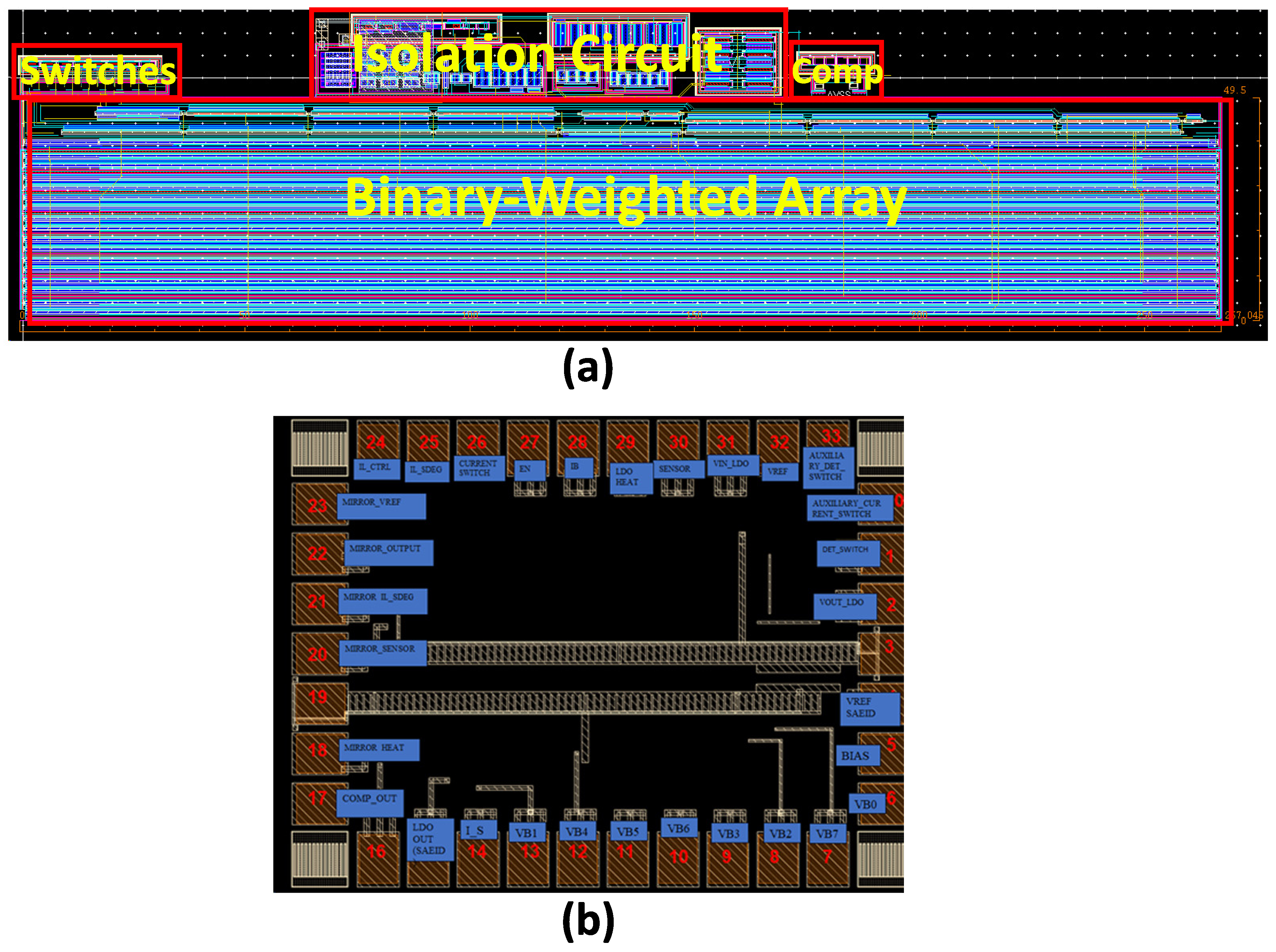
The microscopic view of the manufactured DCDC is shown in Figure 4, including the presence of blocks related to other projects that are not the focus of this article.
It appears that dummy fill is used extensively. However, dummy blockers can be strategically placed to avoid filling certain areas while still meeting density requirements. Each metal and poly layer has a ’dm’ layer that can be used to prevent the script from inserting dummies. Although removing dummy fill may affect the consistency and yield of the etching, it should only be applied to nonsensitive areas. Removing the dummy fill can help reduce some parasitics, depending on the purpose of the circuit.
An , which is determined to be measured, is generated using a programmable two-stage high-side current source circuit from Texas Instruments(TI) [21] and illustrated in Figure 5.
A critical consideration in the design of this circuit is the response characteristics of the NMOS and PMOS transistors employed. These transistors possess large input capacitances, which reduce their response time. Additionally, the node connecting the circuit to the DCDC exhibits high impedance, potentially limiting the final operational speed of the DCDC. A compensation circuit is also implemented to prevent instability due to the feedback loop and to avoid output current oscillation. The current is controlled using the DAC80508 from TI, as described by the following equation:
In this setup, the parameter k denotes the accuracy of the DAC, which can be configured to 12, 14, or 16 bits. The reference voltage is set to 1.25 V using an external resistor divider network. Resistors to are employed to adjust the current and to cancel the DAC output voltage offset.
Voltage sources are required from an on-chip voltage reference to initiate the chip. However, as the design is standalone, TI LDOs, including LP2981I, TPS7A0212, TPS7A0215, TLV75509, TPS7A0212 and TPS7A0218, are utilized. The purpose of these LDOs are as follows, respectively: 3.6 V is used to supply the DAC and op-amp circuit with the necessary voltages, 1.2 V for generating , 1.5 V for setting the reference voltage of the isolation circuit (which can be adjusted as required), 0.9 V as the bias voltage , and 1.8 V as the analog supply voltage for the chip. All of these LDOs will be supplied by a voltage generator that is set to be 5 V. This entire configuration is mounted on a printed circuit board (PCB) shown in Figure 6a. The circuit’s performance is evaluated using the DE2-115 FPGA from TI. To initiate and adjust the DAC code, the Serial Peripheral Interface (SPI) standard is required for communication with the DAC. The core of the SPI is implemented in Verilog and connected to JP4 on the FPGA. Additionally, SAR logic is implemented to control the binary-weighted array, with different voltage logics. The SAR is implemented on FPGA pin JP5 with a voltage of 1.8 V. The Universal Asynchronous Receiver-Transmitter (UART) is implemented on the FPGA to transmit data from the FPGA to a computer. An analog device logic analyzer ensures correct communication between the DAC and the FPGA.
Software developed using QT Designer and Python collects data through the serial port and generates the necessary Excel files.
The operation of the DCDC was evaluated across a range of temperatures. To maintain the circuit at the desired temperature, a test equity half-cubic temperature chamber was utilized. To ensure that the temperature remained at the desired level, a PT1000 sensor was used. The setup of this experiment can be seen in Figure 6c,d.
4. Results
In this section, we present the results of the proposed DCDC design as outlined in the previous sections. Our evaluation encompasses both simulation and experimental data to validate the performance and functionality of the DCDC under various conditions. The analysis includes key metrics such as accuracy, power consumption, and area efficiency, as well as the comparison of theoretical predictions with actual measured outcomes.
The performance of the DCDC was evaluated through a series of experiments, utilizing an 8-bit resolution as implemented with the TSMC 180-nm process. We first discuss the simulation results, which provide an initial validation of the design parameters and functionality. Subsequently, we present the experimental measurements obtained from the fabricated chip, highlighting the operational efficacy of DCDC in practical scenarios.
4.1. Simulations
4.1.1. Process, Local Mismatch and Temperature Sensitivity
To evaluate the sensitivity of the design to process and temperature variations, Monte Carlo simulations are conducted at three temperature corners: -50 °C, 27 °C, and 150 °C, covering the AEC-Q100 Grade 0 temperature range. This approach is necessary for understanding how variations in transistor parameters affect circuit performance. By statistically analyzing thousands of possible variations at each temperature corner, the simulation helps predict and quantify deviations in key performance metrics of the DCDC, including the current deviation of each individual binary branch from its nominal value.
The evaluation process involves fixing the input node of the comparator at a meta-stable position and activating each individual binary-weighted branch. The currents flowing through these branches are adjusted according to their nominal values, with deviations caused by temperature and mismatches accounted for using a voltage-controlled current source (VCCS).
To assess this statistical behavior, a useful parameter is the standard deviation. The standard deviation helps in understanding the shape of the data distribution. For example, in a normal distribution (bell-shaped curve), approximately of the data falls within one standard deviation of the mean, about falls within two standard deviations, and approximately falls within three standard deviations. Monte Carlo simulations typically assume a normal distribution, but deviations from these percentages can indicate non-normal or skewed distributions:
In this equation, represents the standard deviation, N is the number of data points, denotes each individual data point, and is the mean (average) of the data points. By evaluating the current in each branch and calculating the mean and standard deviation (STD), we can assess the effects of process and temperature variations on the circuit’s performance.
This assessment is vital because the circuit operates under the principle of superposition. If the deviations of each individual binary branch remain within specified limits, it ensures that the total error across the entire circuit will also be within acceptable bounds. The superposition principle means that the total error is the sum of the errors from each component, so managing the error of each branch helps keep the overall error within manageable levels. If the total error due to process and temperature variations is less than 1 LSB (Least Significant Bit) in current, then the DCDC’s accuracy is at least as precise as the resolution represented by the LSB.
Furthermore, errors propagate from the MSB to the LSB in a predictable manner. If the MSB error is less than 0.5 LSB, the error in the next MSB bit (second most significant bit) will be less than 0.25 LSB, and this trend continues, with each subsequent bit’s error being half of the previous bit’s error. Therefore, if the MSB error is within 0.5 LSB, the overall system error, including all less significant bits, remains well within the 1 LSB limit. This ensures that the accuracy of the system aligns with the precision level indicated by the LSB.
As specified above, this design covers an application range of to . The total current, determined by downscaling the maximum current , will be . In an -bit DCDC, the current for each bit is calculated using Equation (15):
and,
where to 7, and represents the mirroring index of the branch. For example, at , is with , while the current decreases to with in the smallest branch. These values indicate the nominal current for each bit.
The results of a Monte Carlo simulation with 1000 points at three different temperatures for the three MSB branches, simulated in Specter, are shown in Figure 7.
As stated before, to ensure that the error due to process and temperature variations remains minimal, the deviation of the MSB bit current should be less than half the LSB current. Here, as previously specified, . To achieve 8-bit accuracy, the variation in the MSB bit must satisfy:
In this example, as shown in Figure 7, the worst behavior in terms of mismatch occurs at the coldest temperature. The STD of the MSB current, depicted in Figure 7c, is evaluated to be , and . Following this trend to the lower bits, and . This indicates that as we move to lower bits, the standard deviation decreases proportionally, maintaining the required accuracy for an 8-bit design. Table 1 shows the complete values for every individual bit in terms of STD and mean.
The observed variations are closely associated with the dimensions of the base transistors. According to Equation (17):
where W and L represent the width and length of the transistor, respectively, and A is a constant specific to a particular parameter, such as current, provided in the Process Design Kit (PDK) [20]. As the dimensions of the transistor increase, the mismatch decreases, thereby improving the overall performance and reliability of the circuit.
4.1.2. Transient
To accurately assess the performance of an Analog-to-Digital Converter (ADC), it is essential to examine two critical parameters: Integral Non-Linearity (INL) and Differential Non-Linearity (DNL). These parameters can be effectively evaluated using a ramp test.
Integral Non-Linearity (INL) quantifies the deviation of the actual ADC transfer function from an ideal straight line that represents the expected linear response. During a ramp test, a linearly increasing or decreasing input signal is applied to the ADC, and the output is recorded. INL at a given code k is defined as:
where is the actual output voltage corresponding to the digital code k, and is the ideal output voltage for that code. A high INL value indicates significant deviations from linearity, leading to errors in the conversion process. As a result, INL directly impacts the overall accuracy of the ADC by introducing systematic errors throughout the input range.
Differential Non-Linearity (DNL) measures the deviation between the actual and ideal step sizes between adjacent digital codes. The DNL at a specific code k is expressed as:
where represents the actual step size between codes k and , and is the ideal step size. In a ramp test, by carefully analyzing these step sizes as the input voltage increases or decreases, one can calculate the DNL for each code. High DNL values can result in missing codes, where certain input levels do not correspond to any digital code, potentially leading to data loss. Therefore, DNL primarily affects the precision of the ADC by ensuring the consistency and uniformity of the conversion steps.
Relationship and Accuracy Implications: The ramp test is instrumental in identifying and quantifying INL and DNL, which are closely related to the ADC’s accuracy and precision. INL affects the overall accuracy by indicating how much the ADC’s output deviates from an ideal linear response, with lower INL values reflecting higher accuracy. DNL affects the ADC’s precision by ensuring that each step in the input voltage is consistently represented in the digital output. Minimizing both INL and DNL is crucial for achieving reliable, accurate, and precise analog-to-digital conversion.
these points should be considered to understand the INL and DNL curves:
Evaluate INL:
- Check for Maximum Deviation: Identify the points on the INL curve where the deviation is largest (positive or negative), showing the worst-case non-linearity.
- Linearity: Ideally, the INL curve should be as flat as possible. A flat INL indicates good linearity of the ADC across its entire input range.
- Systematic Errors: Look for systematic trends in the INL curve (e.g., consistently increasing or decreasing), which may indicate issues in the ADC design or external influences like power supply variations.
Evaluate DNL:
- Uniformity of Steps: Analyze how close the DNL values are to zero. A DNL of zero means the step sizes are uniform, which is ideal.
- Check for Missing Codes: If DNL at any point, it indicates a missing code, meaning some input ranges are not represented in the output.
- Random Noise vs. Systematic Errors: Random variations in DNL might indicate noise, whereas consistent patterns could suggest systematic errors in the ADC design.
Interpret Results:
- Good ADC Performance: A good ADC will have INL and DNL close to zero across the entire input range, indicating accurate and precise conversion.
- Poor ADC Performance: Large deviations in INL or DNL, especially in certain regions, suggest potential problems in the ADC’s design or implementation, leading to inaccuracies.
In this example, the input of the DCDC was transferred from to , in the worst corner of the Monte Carlo simulation, that is, the corner with the largest mismatch in three different temperatures. One consideration for testing the performance of the DCDC is the clock speed of the SAR logic. According to Figure 1, the input node of the comparator is a high impedance node and has a large parasitic capacitor . To ensure that the conversion is performed correctly, the voltage of this node should settle according to the capacitor voltage Equation (20):
where:
As I has a higher value, it changes more quickly with time, resulting in faster voltage settling. However, with smaller currents, it takes longer to settle. To avoid any missing codes, this should be carefully considered. The internal dynamics of the circuit during conversion can be illustrated in Figure 9.
Figure 8.
Transient behavior of the nodes involved in the conversion process. From the moment the SAR logic triggers bit (bit 7), it takes approximately 430 ns for the output to stabilize.
Figure 8.
Transient behavior of the nodes involved in the conversion process. From the moment the SAR logic triggers bit (bit 7), it takes approximately 430 ns for the output to stabilize.
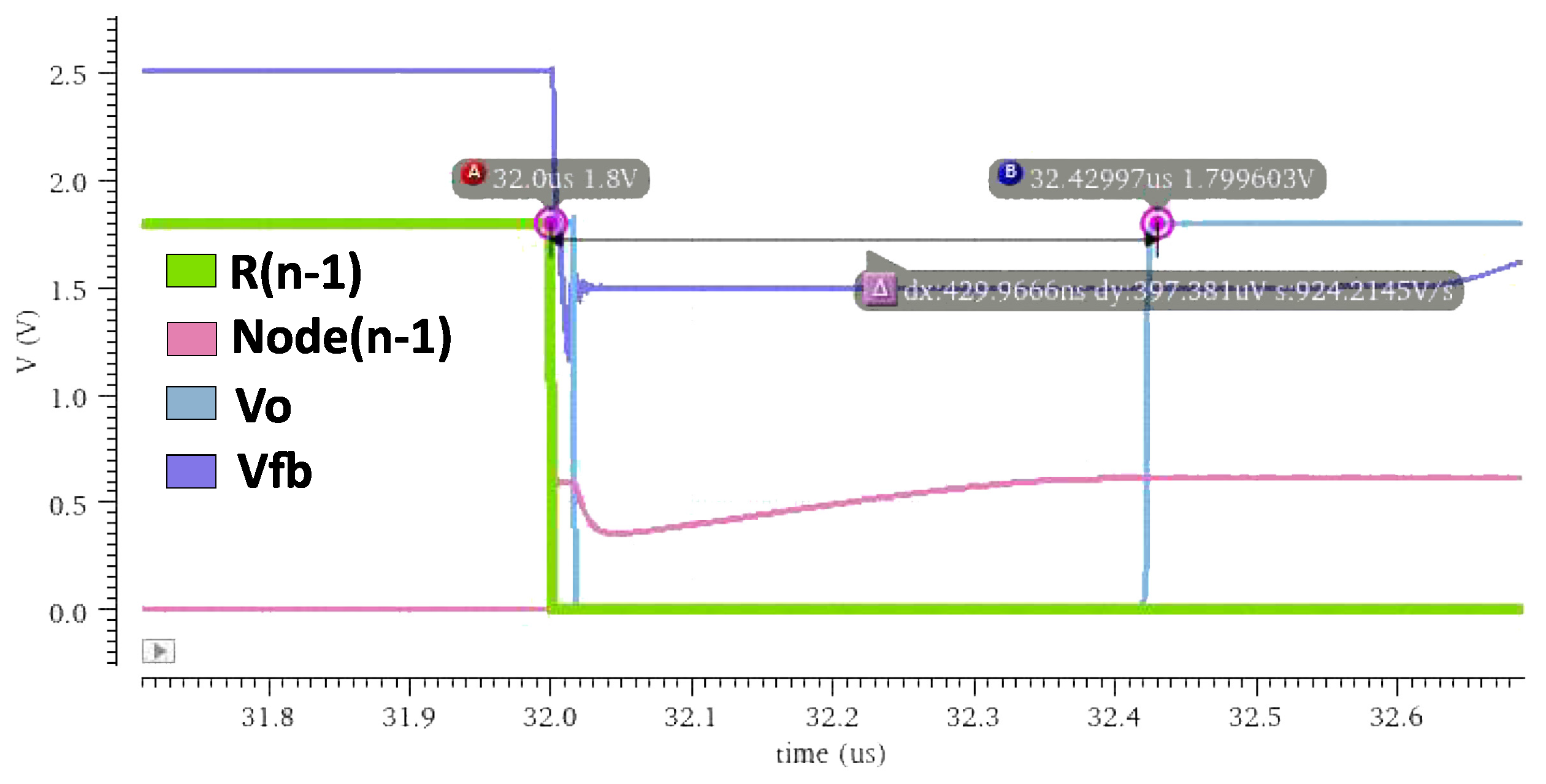
Figure 9.
(a) DNL and (b) INL of the post-layout simulation.
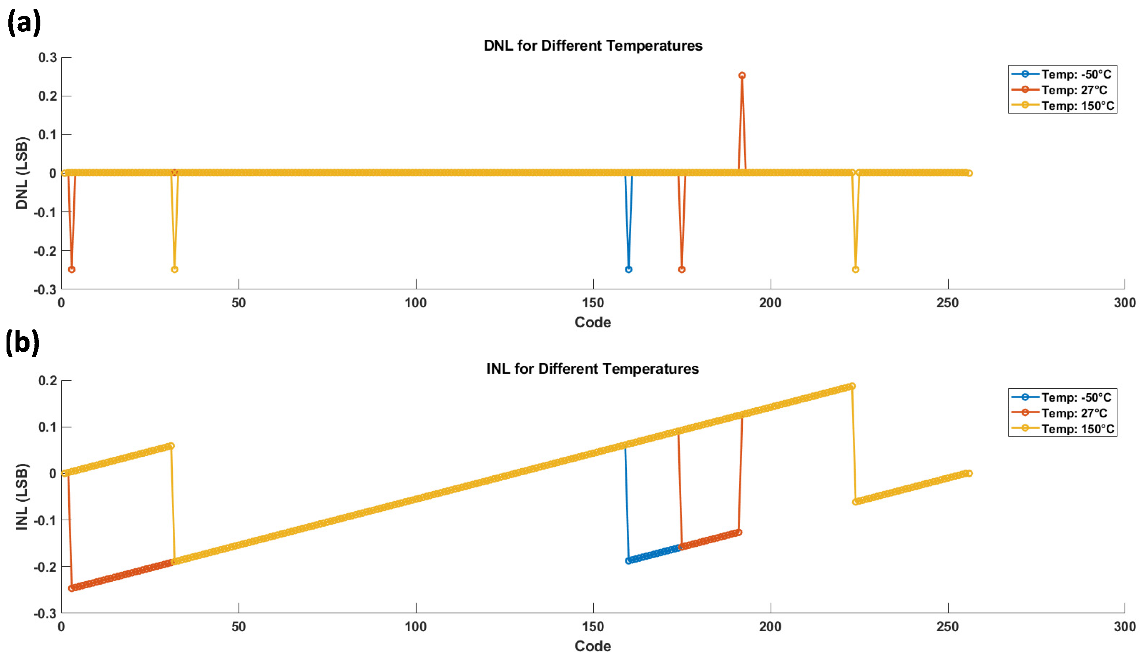
Considering this in the conversion, the INL and DNL plot in is shown according to the post-layout simulation results.
4.2. Measurement
4.2.1. Ramp Test
As stated in the Simulation section, the Ramp test is one of the most effective methods to evaluate the performance of an ADC. To perform this test, the test bench shown in Figure 7 is used, where a gradual voltage change is applied to achieve a gradual current change with 14-bit accuracy, resulting in 64 hits.
This evaluation is conducted at different clock speeds and temperatures, specifically at -10 °C and 100 °C in a temperature chamber, and at room temperature, as shown in Figure 6b–d. The reason for not testing at higher and lower temperatures stems from two limitations: the components on the PCB are designed to operate between -25 °C and 125 °C, and the temperature chamber operates between -40 °C and 130 °C.
Another option to control the temperature would be to use a micro-bath, but the oil used in a micro-bath is prohibitively expensive and begins to evaporate at 125 ° C. Since our goal was to measure performance under hot and cold conditions rather than precise temperature control, we ensured that the temperature of the die was sufficiently hot and cold for this purpose.
The state machine governing the measurement process during the ramp test is illustrated in Figure 10.
The conversion results at different clock speeds are presented as INL and DNL plots in Figure 11.
Based on the analysis of the test bench, we have determined that to maintain the desired accuracy, the system should operate at a clock speed of 25 kHz. This clock speed ensures that the deviations remain within acceptable limits, specifically under LSB, as shown in the previous figures.
To further evaluate the performance under different temperature conditions, we conducted tests at -10°C and 100°C. The results at these temperatures were also plotted for INL and DNL using the 25 kHz clock speed, as this configuration provided the most reliable accuracy in our initial testing. The following figures present the INL and DNL plots for these extreme temperature conditions, ensuring that the system maintains its accuracy in a wide range of operating environments Figure 12.
From this evaluation, the INL and DNL curves at a clock speed of 25 kHz and room temperature indicate that the system achieves an accuracy within 1 LSB, suggesting that 8-bit accuracy is maintained under these conditions. However, as the clock speed increases, the accuracy diminishes. This reduction in precision is likely due to the capacitive effects in the circuit, as depicted in Figure 7.
Another trend verified in the measurements, which was also predicted by the simulations, is that the sensor exhibits better performance at higher temperatures compared to colder temperatures. This can be concluded by comparing the DNL curves at different temperatures: at -10°C, the DNL deviation is around LSB, at room temperature it decreases to LSB, and at 100 ° C it improves further to LSB.
4.2.2. Spectrum Test
The spectrum test is a dynamic evaluation method used to assess the performance of DCDCs by analyzing the frequency domain of the converter’s output when subjected to a known input signal, usually a sine wave. This test is particularly effective in identifying frequency-related issues like harmonic distortion, spurious tones, and noise characteristics that may not be apparent through time-domain analysis. The key parameters evaluated include Signal-to-Noise Ratio (SNR), Spurious-Free Dynamic Range (SFDR), and Total Harmonic Distortion (THD). These metrics are crucial to ensuring the converter’s ability to maintain signal fidelity and accuracy, especially in high-frequency or rapidly changing signal environments.
To evaluate the dynamic performance of the DCDC, a spectrum analysis was performed using a coherent sampling approach. Coherent sampling is a technique used in ADC testing where the input sine wave frequency is chosen so that an integer number of sine wave cycles fits exactly into the time window of the data acquisition. This ensures that the sampled data do not have any discontinuities at the beginning and end of the acquisition window, which could cause spectral leakage and distort the frequency spectrum.
The relationship between the parameters for coherent sampling is given by:
where - J is the number of sine wave cycles within the sampling window, - M is the number of samples, - is the frequency of the input signal, and - is the sampling frequency.
The sampling frequency is determined by the following equation:
where - is the clock frequency, and - n represents the resolution (in bits) of the DCDC.
Coherent Sampling Setup
The following steps were taken to set up the coherent sampling:
Input Signal Generation: A sine wave signal was generated in MATLAB with a peak-to-peak amplitude slightly lower than the maximum current that the DCDC could handle. The frequency of the sine wave was selected so that an integer number of cycles would fit exactly within the data acquisition time window. This ensured that the sampled data did not contain any discontinuities at the beginning or end of the acquisition window, thereby preventing spectral leakage.
Conversion to DAC Codes: The generated sine wave current signal was converted into corresponding DAC input codes using Equation (12). These codes were then programmed into the DAC via the FPGA.
Spectrum Analysis Procedure
Data Acquisition: The output of the DCDC, after the sine wave signal was input, was collected, and preprocessing was carried out to remove any potential noise or artifacts from the data. The mean (average) of the signal was calculated as follows:
where - is the mean of the signal, - N is the total number of samples, and - represents the n-th sample of the signal.
The signal was then adjusted by subtracting the calculated mean:
where - is the mean-adjusted (processed) signal.
FFT and Magnitude Spectrum: The preprocessed data, now centered around zero, was transformed from the time domain to the frequency domain using the Fast Fourier Transform (FFT):
where - is the k-th frequency component in the spectrum, and - represents the complex exponential component of the FFT.
From the resulting frequency spectrum, key parameters were calculated. The fundamental power, which represents the main signal component, was determined as:
where - is the power of the fundamental frequency component, - corresponds to the index of the fundamental frequency, and - represents the squared magnitude of the fundamental frequency component.
The noise power, excluding the fundamental component, was calculated by summing the remaining power in the spectrum:
where - is the total noise power, - represents the total power of all frequency components excluding the fundamental frequency.
Using these values, the Signal-to-Noise Ratio (SNR) was calculated:
Spurious-Free Dynamic Range (SFDR): The SFDR was determined as follows:
where - distortion represents the power of the most significant spurious tone or distortion in the signal.
Effective Number of Bits (ENOB): Finally, the Effective Number of Bits (ENOB) was derived from the SNR:
Analysis of Results: The spectrum analysis provided insights into the DCDC’s ability to accurately convert the input signal without introducing significant noise or distortion. The results, characterized by a clean spectrum with minimal artifacts, confirmed that the DCDC performed as expected under the test conditions.
This systematic approach to spectrum analysis allowed for a thorough evaluation of the DCDC’s dynamic performance, ensuring that it met the required specifications for accurate and reliable current-to-digital conversion.
The result of the processing measured data is shown in Figure 13:
The ENOB of 7.21 bits reflects the resolution of the DCDC converter, taking into account both noise and distortion. An ENOB of 7.21 bits suggests that the DCDC operates close to its theoretical maximum resolution of 8 bits, with minimal degradation due to noise and distortion.
4.3. Comparison and Discussion
4.3.1. DxDCs Comparision
Although the converters compared in Table 2:
serve different purposes -[15] being a Light-Dose-To-Digital Converter and [16] a temperature-to-digital converter - the type and application of these converters differ, the comparison focuses on common critical parameters such as power consumption, area and energy efficiency, which are relevant across various DxDC designs.
This work demonstrates an energy per conversion of 1.52 pJ and power consumption of 117 µW. In comparison, [16], despite its different application, exhibits an energy per conversion of about 9 nJ and power consumption of 2250 µW. This highlights the significant energy efficiency of the proposed design. Additionally, while [15] operates in a smaller process node (65 nm vs. 180 nm), our design achieves a significantly smaller area (0.016 mm² vs. 1.71 mm²). These metrics underscore the efficiency and compactness of our approach, making it particularly suitable for low-power and space-constrained applications, despite differences in their functional domains.
4.3.2. Area
The total area occupied by the DCDC, as shown in the layout in Figure 3, is 0.016 in a 180 technology. The primary goal of this design is to eliminate the need for standalone ADCs and thick film resistors to convert current to voltage and then to a digital signal. For comparison, an ultra-small sigma-delta ADC introduced by Taylor [22] occupies 0.07 in a 65 technology, demonstrating a 4.375 times improvement in area efficiency, even before considering the scaling factor between the technologies.
Traditional designs often require thin-film resistors to convert current to voltage. For instance, a typical thin-film resistor, such as a 10 k resistor in a 65 nm technology, can occupy approximately 0.04 mm² [23]. In contrast, our design achieves the same functionality without the need for such resistors, thus saving valuable area on the chip.
Moreover, in a SoC environment, where multiple instances of this structure may be required, replicating our design further reduces the overall area consumption compared to traditional approaches that would necessitate additional resistors and ADCs. This highlights the scalability and efficiency of our approach, particularly in large-scale integrated systems.
4.3.3. Power Consumption
The total power consumption of the chip in the worst-case scenario has been evaluated to be 0.144 mW. This figure encompasses all the power drawn from the DC voltage source within the circuit. Notably, approximately two-thirds of this power consumption originates from the isolation op-amp, which was fabricated without optimization. It is estimated that by using an op-amp specifically designed for this structure, the power consumption could be reduced by 50%.
In comparison, Taylor’s ADC [22] demonstrates a power consumption of 8 mW in its most power-efficient configuration. Even with the current non-optimized design, our approach offers a significant reduction, with a 55.5-fold decrease in power consumption. This dramatic reduction highlights the efficiency of our design, especially in applications within System-on-Chip (SoC) environments where precise current measurement is critical. This efficiency not only conserves energy but also minimizes heat generation, which is essential for maintaining the reliability and longevity of the SoC components.
5. Conclusions
In this paper, we introduced a systematic approach to designing a Direct Current-to-Digital Converter (DCDC), exemplified through an 8-bit implementation aimed at advanced current measurement in System-on-Chip (SoC) applications. The proposed DCDC leverages a current mirror in a cascode topology, integrated with Successive Approximation Register (SAR) logic, to achieve precise 8-bit resolution without the need for nonlinearity calibration. Fabricated using the TSMC 180 nm process, this design showcases exceptional performance, including an energy per conversion of 1.52 pJ, power consumption of 117 µW, and a compact total area of just 0.016 mm².
The results from both simulations and experimental evaluations validate the effectiveness of this design across various operating conditions, including extreme temperatures, confirming that the DCDC maintains accuracy within 1 LSB at different clock speeds and environmental conditions. The comparison with other DxDCs highlights the superior energy efficiency and compactness of our design, making it particularly suitable for low-power, space-constrained applications.
This work addresses the challenges of traditional current measurement methods by providing a scalable and efficient solution that eliminates the need for standalone ADCs and thick-film resistors. The DCDC’s capability for online measurements during both standard operations and in-field conditions significantly enhances the performance and reliability of SoCs, setting a new benchmark for future developments in semiconductor technologies.
Overall, the introduction of this systematic approach to DCDC design, illustrated through the 8-bit example, marks a significant advancement in current measurement technologies, offering a robust and reliable solution for modern SoC designs. Its integration into various SoC platforms has the potential to extend operational lifespans and improve the dependability of integrated circuits across diverse applications.
References
- Ji, Z.; Chen, H.; Li, X. Design for reliability with the advanced integrated circuit (IC) technology: challenges and opportunities. Sci. China Inf. Sci. 2019, 62, 226401. [Google Scholar] [CrossRef]
- Ghani, T.; Armstrong, M.; Auth, C.; Bost, M.; Charvat, P.; Glass, G.; Hoffmann, T.; Johnson, K.; Kenyon, C.; Klaus, J.; McIntyre, B.; Mistry, K.; Murthy, A.; Sandford, J.; Silberstein, M.; Sivakumar, S.; Smith, P.; Zawadzki, K.; Thompson, S.; Bohr, M. A 90nm high volume manufacturing logic technology featuring novel 45nm gate length strained silicon CMOS transistors. IEEE International Electron Devices Meeting 2003 2003, 11.6.1–11.6.3. [CrossRef]
- Porter, M.; Erich, R.; Ricotta, M. Medical Electronics Design, Manufacturing, and Reliability. In Materials for Advanced Packaging; Lu, D., Wong, C.P., Eds.; Springer International Publishing: Cham, 2017; pp. 767–811. [Google Scholar] [CrossRef]
- Dobbelaere, W.; Colle, F.; Coyette, A.; Vanhooren, R.; Xama, N.; Gomez, J.; Gielen, G. Applying Vstress and defect activation coverage to produce zero-defect mixed-signal automotive ICs. 2019 IEEE International Test Conference (ITC) 2019, 1–4. [Google Scholar] [CrossRef]
- Yu, Q.; Zhang, Z.; Dofe, J. Investigating Reliability and Security of Integrated Circuits and Systems. 2018 IEEE Computer Society Annual Symposium on VLSI (ISVLSI) 2018, 106–111. [Google Scholar] [CrossRef]
- Darko, E.N.; Bhatheja, K.; Adjei, D.; Strong, M.; Chen, D. On-Chip Monitoring of Time-Dependent Dielectric Breakdown (TDDB) using a Novel Leakage Current Sensor with Digital Output. 2023 IEEE International Integrated Reliability Workshop (IIRW) 2023, 1–6. [Google Scholar] [CrossRef]
- Udaya Shankar, S.; Kalpana, P. Reliability and Circuit Timing Analysis with HCI and NBTI. In Advances in VLSI, Communication, and Signal Processing; Harvey, D., Kar, H., Verma, S., Bhadauria, V., Eds.; Springer Singapore: Singapore, 2021; pp. 371–392. ISBN 978-981-15-6840-4. [Google Scholar]
- Saniç, M.T.; Yelten, M.B. Time-dependent dielectric breakdown (TDDB) reliability analysis of CMOS analog and radio frequency (RF) circuits. Analog Integrated Circuits and Signal Processing 2018, 97, 39–47. [Google Scholar] [CrossRef]
- Zhao, X.; Wan, Y.; Scheuermann, M.; Lim, S.K. Transient modeling of TSV-wire electromigration and lifetime analysis of power distribution network for 3D ICs. 2013 IEEE/ACM International Conference on Computer-Aided Design (ICCAD) 2013, 363–370. [CrossRef]
- Dong, Z.; Sun, Z.; Yang, X.; Li, X.; Xue, Y.; Luo, C.; Cai, P.; Wang, Z.; Wang, S.; Zhang, Y.; Wang, C.; Ren, P.; Ji, Z.; Wu, X.; Wang, R.; Huang, R. Catching the Missing EM Consequence in Soft Breakdown Reliability in Advanced FinFETs: Impacts of Self-heating, On-State TDDB, and Layout Dependence. 2023 IEEE Symposium on VLSI Technology and Circuits (VLSI Technology and Circuits) 2023, 1–2. [CrossRef]
- de Orio, R.L.; Ceric, H.; Selberherr, S. Physically based models of electromigration: From Black’s equation to modern TCAD models. Microelectronics Reliability 2010, 50, 775–789. Available online: https://www.sciencedirect.com/science/article/pii/S0026271410000193 (accessed on 1 January 2024). [CrossRef]
- Bui, T. Why Low Quiescent Current Matters for Longer Battery Life. Available online: https://www.analog.com/media/en/technical-documentation/technical-articles/why-low-quiescent-current-matters-for-longer-battery-life.pdf (accessed on 1 January 2024).
- Yi, S.-C. A 10-bit current-steering CMOS digital to analog converter. AEU - International Journal of Electronics and Communications 2015, 69, 14–17. Available online: https://www.sciencedirect.com/science/article/pii/S1434841114002003 (accessed on 1 January 2024). [CrossRef]
- Khan, D.; Basim, M.; Ain, Q.u.; Shah, S.A.A.; Shehzad, K.; Verma, D.; Lee, K.-Y. Design of a Power Regulated Circuit with Multiple LDOs for SoC Applications. Electronics 2022, 11, 2774. [Google Scholar] [CrossRef]
- Lee, I.; Moon, E.; Kim, Y.; Phillips, J.; Blaauw, D. A 10mm3 Light-Dose Sensing IoT2 System With 35-To-339nW 10-To-300klx Light-Dose-To-Digital Converter. In 2019 Symposium on VLSI Circuits; IEEE, 2019; pp. C180–C181. [CrossRef]
- Ganji, M.; Saikiran, M.; Chen, D. A Wide-Range Low-cost Temperature to Digital Converter Independent of Device Models. In Proceedings of the 2022 IEEE International Symposium on Circuits and Systems (ISCAS); IEEE, 2022; pp. 605–609. [Google Scholar] [CrossRef]
- Kashmiri, S.M.; Xia, S.; Makinwa, K.A.A. A Temperature-to-Digital Converter Based on an Optimized Electrothermal Filter. IEEE Journal of Solid-State Circuits 2009, 44, 2026–2035. [Google Scholar] [CrossRef]
- Banba, H.; Shiga, H.; Umezawa, A.; Miyaba, T.; Tanzawa, T.; Atsumi, S.; Sakui, K. A CMOS bandgap reference circuit with sub-1-V operation. IEEE Journal of Solid-State Circuits 1999, 34, 670–674. [Google Scholar] [CrossRef]
- Sekyere, M.; Bruce, I.; Yang, R.; Chen, D.; McAndrew, C. C.; Jin, X.; He, C.; Garrity, D. Matching Critical Analog Circuit Components Up to 3rd Order Gradients for All Possible Exact Matching Ratios. IEEE Transactions on Computer-Aided Design of Integrated Circuits and Systems 2024, 1, 1–1. [Google Scholar] [CrossRef]
- Sekyere, M.; Darko, E.N.; Bruce, I.; Odion, E.O.; Bhatheja, K.; Chen, D. Ultra-Small Area, Highly Linear Sub-Radix R-2R Digital-To-Analog Converters with Novel Calibration Algorithm. In Proceedings of the 2023 IEEE 66th International Midwest Symposium on Circuits and Systems (MWSCAS); 2023; pp. 604–608. [Google Scholar] [CrossRef]
- Texas Instruments. Available online: https://www.ti.com/lit/an/slaa867/slaa867.pdf (accessed on 18 August 2024).
- Taylor, G.; Galton, I. A Reconfigurable Mostly-Digital Delta-Sigma ADC With a Worst-Case FOM of 160 dB. IEEE Journal of Solid-State Circuits 2013, 48, 983–995. [Google Scholar] [CrossRef]
- Zogbi, D. Thin Film Resistors: A Bright Future for Precision Components, Integration and Miniaturization. TTI MarketEye, 2015. Available online: https://www.tti.com/content/ttiinc/en/resources/marketeye/categories/passives/me-zogbi-20150424.html?srsltid=AfmBOopBu-JdOHM28LVEoVPXkgQy_sG9RJ7Vu16JmuQjz4BWaSiLo2jZ.
- Zhurang Zhao, Embedded Linearity Test for ADCs, Master’s thesis, University of British Columbia, March 2001.
Figure 1.
Conceptual overview of the DCDC design, divided into seven key sections: (I) Biasing circuit and reference current generation using a Banba band-gap voltage reference [18], (II) Switch array controlling gate-switching of cascade transistors via NOT gates, (III) SAR logic for controlling the switch array, (IV) Binary-weighted array for reflecting the reference current, (V) Isolation circuit separating the main and active nodes, (VI) Current generation within the SOC for DCDC measurement, and (VII) Comparator composed of two series-connected inverters.
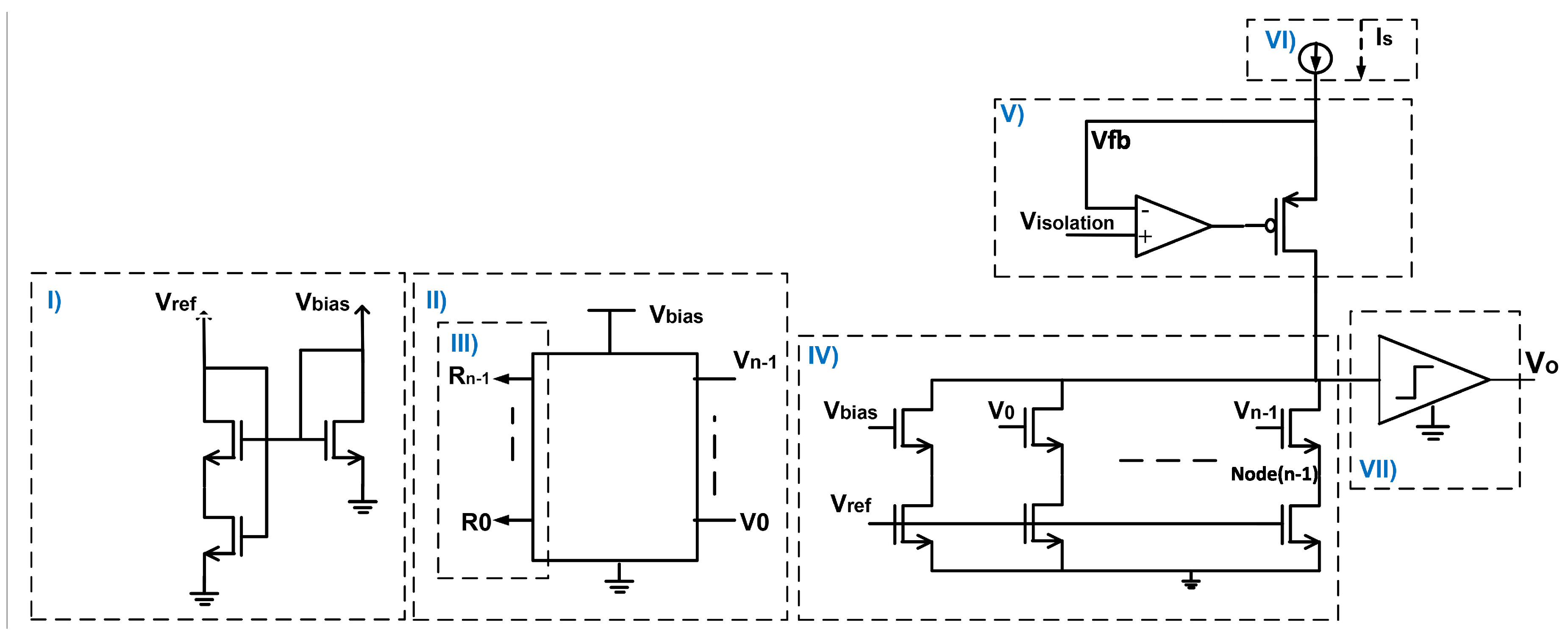
Figure 2.
Schematic of the DCDC operation. The size of the base transistor, , regulates the voltage and the current, , and must be "comfortably in saturation," implying to . The mechanism aims to solve for , and at the conclusion of the conversion, it is expected to achieve , with the structure settling into a meta-stable balance at .
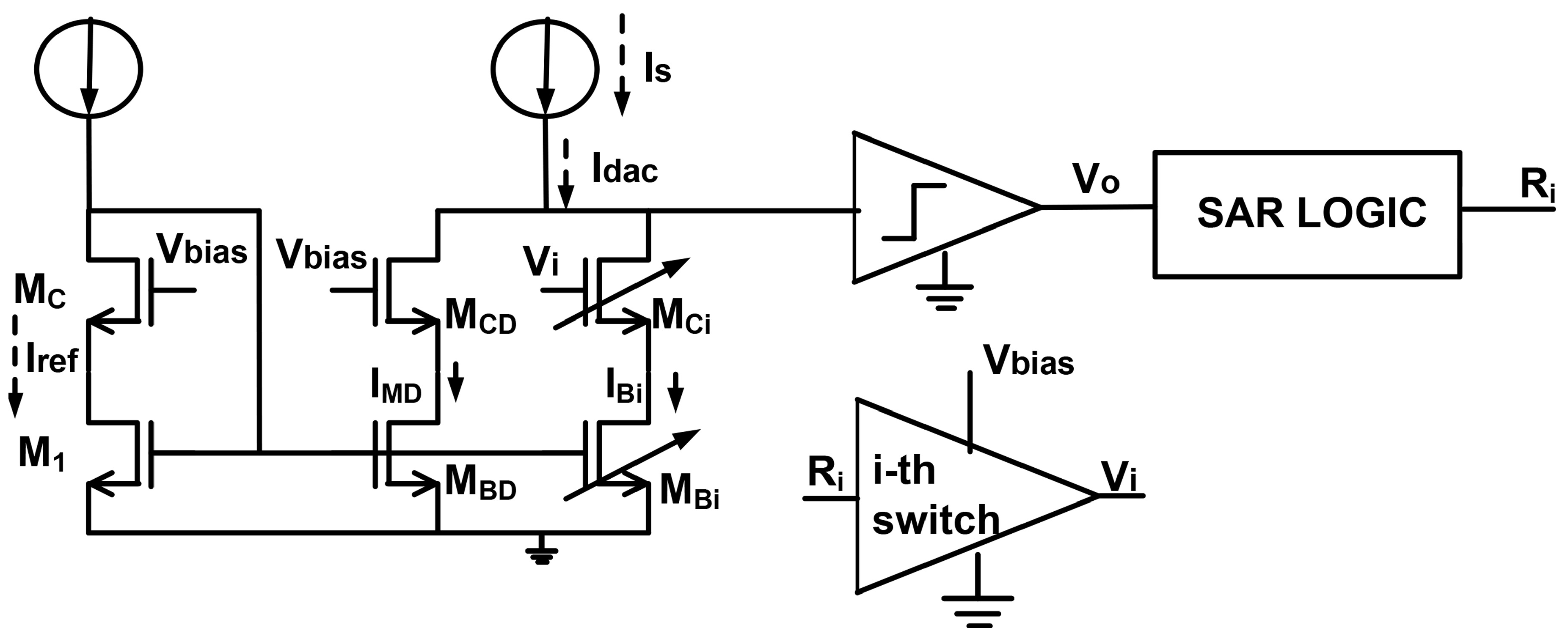
Figure 4.
Microscopic view of the die: (a) As it can be seen, there are four quadrant on the die, and only quadrant C is bonded, (b) and (C) shows the scaled view of the quadrant C, in which DCDC is fabricated.
Figure 4.
Microscopic view of the die: (a) As it can be seen, there are four quadrant on the die, and only quadrant C is bonded, (b) and (C) shows the scaled view of the quadrant C, in which DCDC is fabricated.
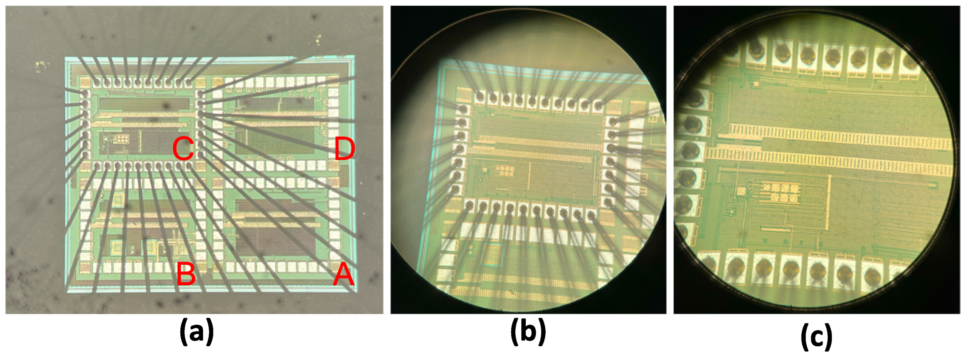
Figure 5.
This schematic diagram represents a current source circuit integrated with a DAC for precise voltage control. The design features N-channel and P-channel MOSFETs (, ), which work in conjunction with differential amplifiers (, ) and resistive feedback networks (, , ) to regulate the output current. The DAC provides a reference voltage (), ensuring the circuit maintains stability and accuracy across varying supply voltages (, ). is the reference voltage of the DCDC. This configuration is optimized for low-noise performance, making it ideal for applications requiring high precision and reliability [21].
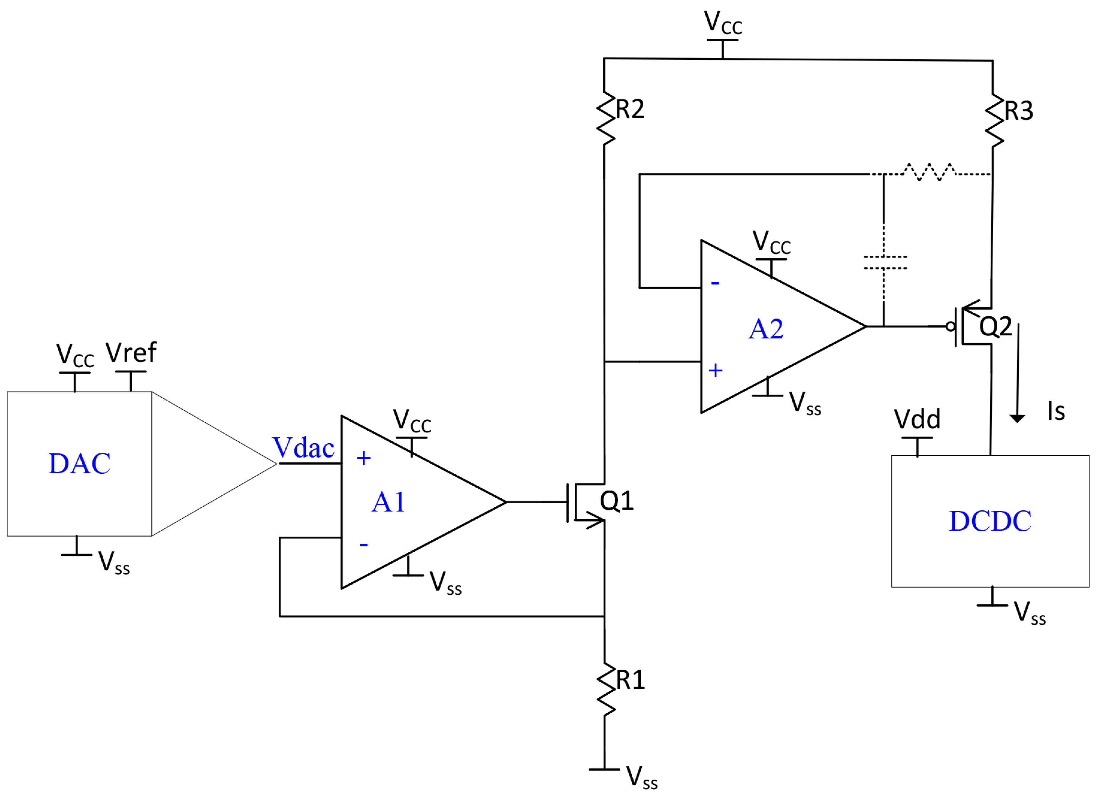
Figure 6.
The measurement setups are presented as follows: (a) The PCB of the test circuit is shown. As depicted in the photograph, an external 5V power supply is connected to the power lock connector of the circuit. The power management section on the PCB ensures that both the DCDC and the test circuit receive the required supply voltages. The current control circuit from TI is utilized [21]. The DUT is driven by the FPGA through two XH connectors: the top connector drives the SPI, while the bottom connector drives the SAR logic. (b) The circuit is tested in the presence of the FPGA. The pins specified for any connections on the FPGA are revealed. An RS232 to USB converter cable delivers data to the computer through UART. A logic analyzer from Analog Devices is used to monitor the SPI communication between the SPI and FPGA. (c) A temperature chamber is used to evaluate the operation of the DCDC under hot and cold conditions. A PT1000 sensor is utilized to measure the temperature at the top of the die. (d) The setup inside the chamber is shown. The DUT is placed on one side, with the FPGA and external voltage source connected to it. The PT1000 ensures that the temperature on the die remains at the desired level during testing.
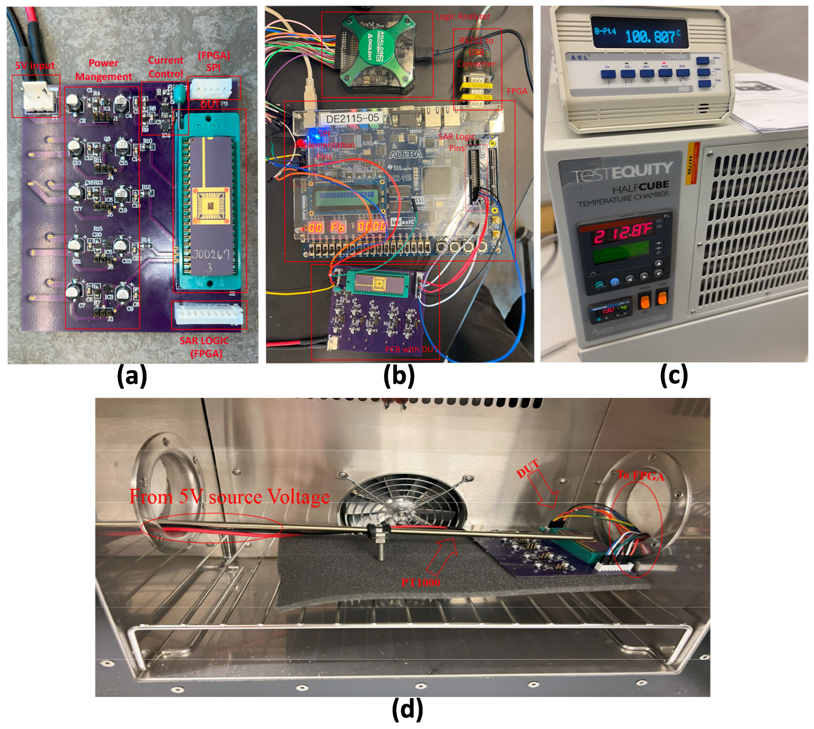
Figure 7.
This figure illustrates the current deviations caused by mismatches in the branches of (a) bit 5, (b) bit 6, and (c) bit 7, along with their respective mirroring ratios in (d), (e), and (f). To achieve the desired level of accuracy, each branch must maintain its corresponding current within the range defined by the LSB weight.
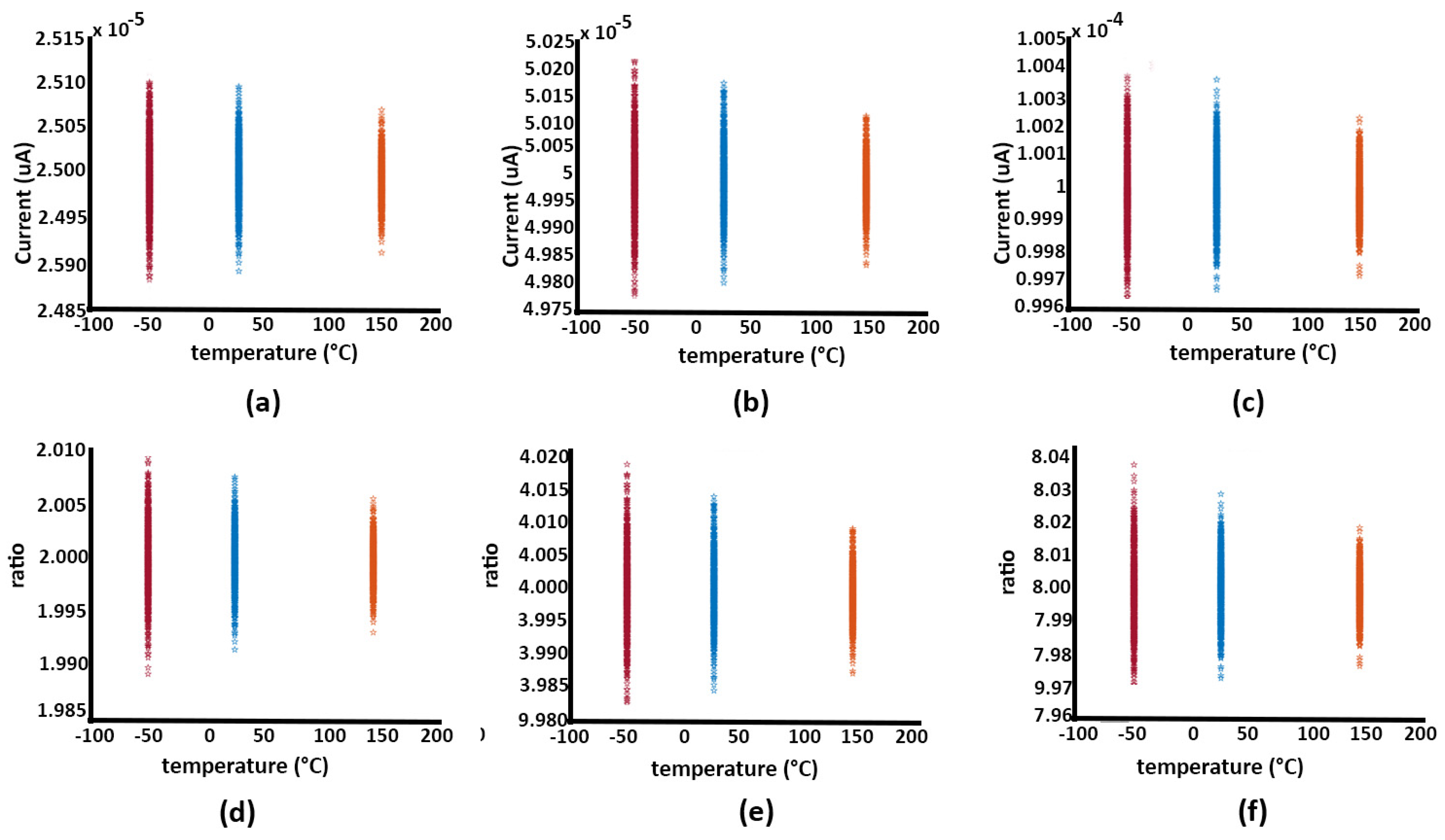
Figure 10.
The state machine of the ramp conversion is shown here: The process starts with system initialization in the ‘Start’ and ‘INIT’ states, followed by writing an initial value of zero to the DAC in ‘Write_DAC’. The ‘Check_write’ state verifies the correct value, and ‘Start SAR’ initiates the SAR logic for conversion. The speed of the conversion is determined here. After waiting in ‘Wait’, the result is sent via UART (‘SEND UART’), and the DAC value is incremented (‘Increment’). The cycle repeats until full scale is reached, concluding in the ‘END’ state.
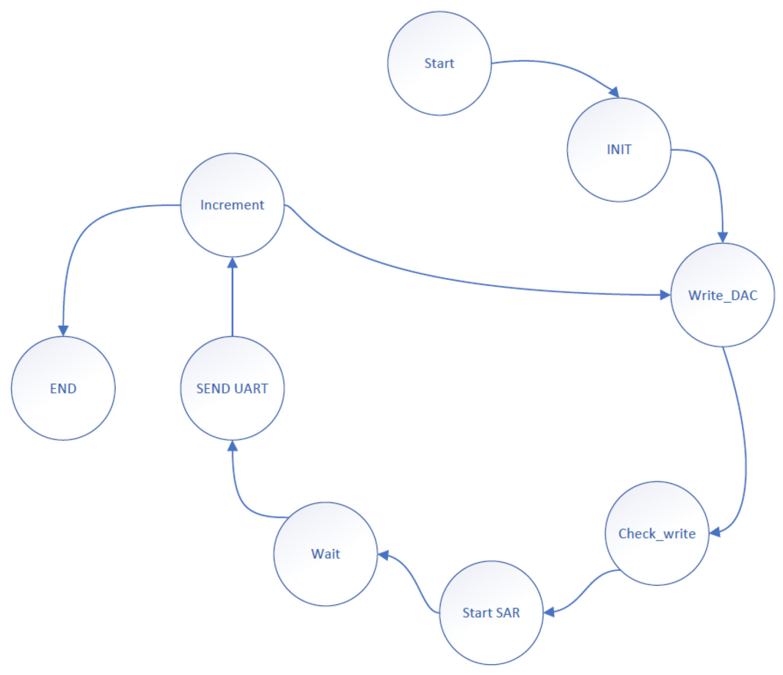
Figure 11.
INL and DNL curve is shown here: a) shows the DNL plots at 25 kHz and 50 kHz SAR clock speeds, respectively, both measured at room temperature. The observed deviation is within LSB at 25 kHz, which is likely attributed to the test bench setup. However, at 50 kHz, missing codes appear, and the deviation increases, indicating reduced accuracy. This limitation arises from the setup’s ability to handle higher speeds. (b) shows the corresponding INL plots at 25 kHz and 50 kHz, respectively.
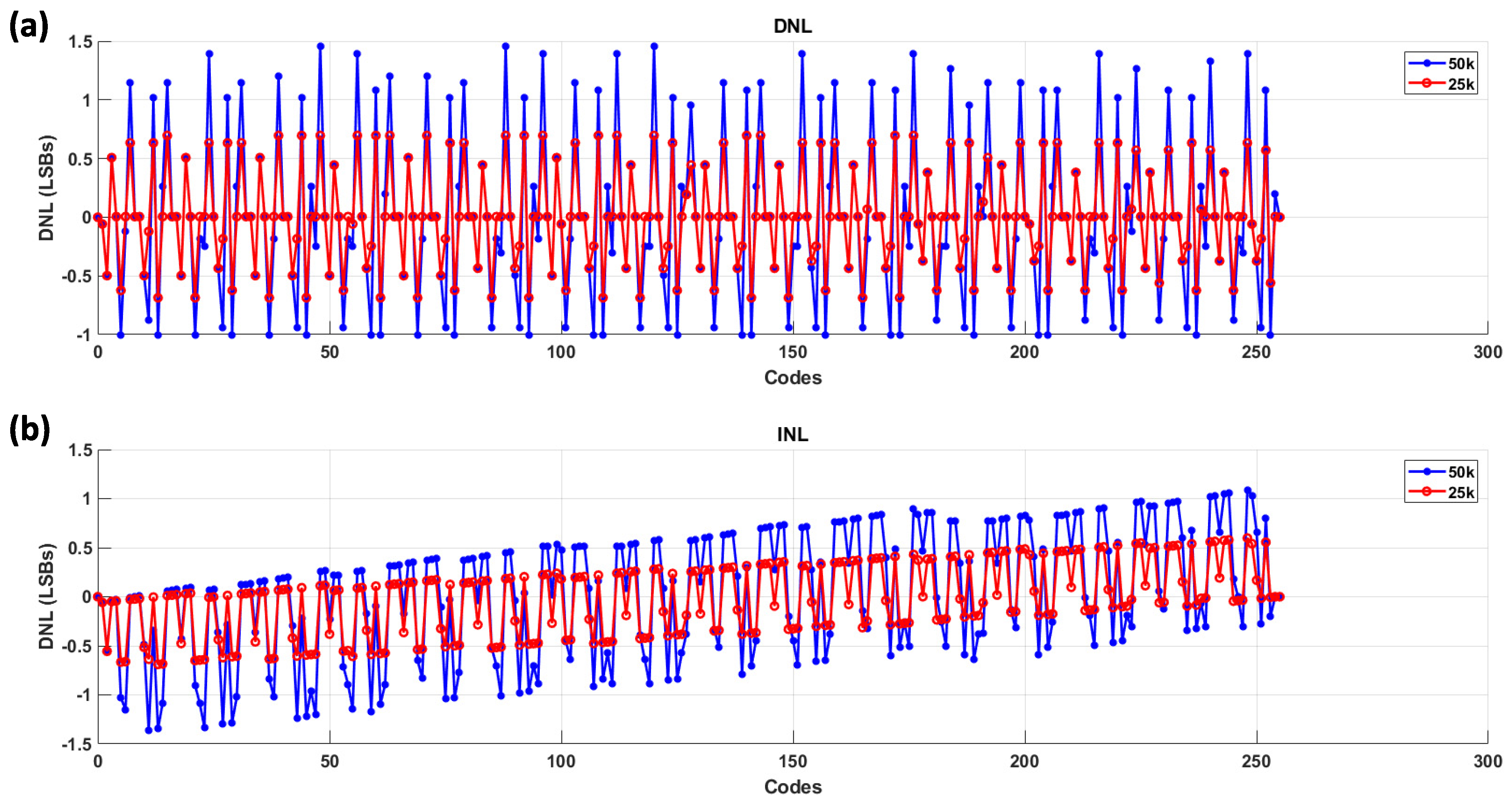
Figure 12.
(a) DNL plots at -10°C and 100°C, measured at 25 kHz SAR clock speed. The results indicate that the DNL deviation remains within LSB for the cold temperature, and less than LSB for the hot temperature. (b) INL plots at -10°C and 100°C under the same conditions. The INL curve shows a slight increase with code number, but the variation remains within acceptable limits, ensuring that the system maintains its accuracy across these temperature extremes.
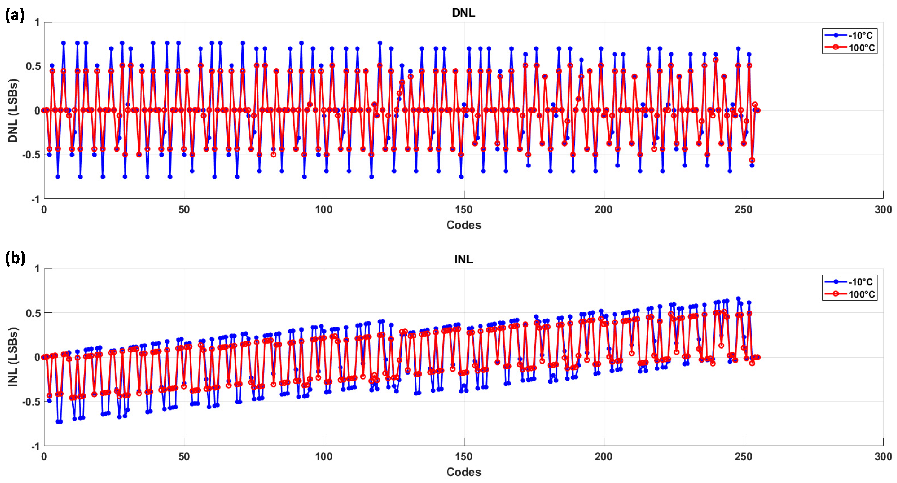
Figure 13.
The process of generating DAC code and performing spectrum analysis of the processed output is shown as follows: (a) A sine wave representing the current, which needs to be fed into the sensor, is depicted here. This sine wave covers a range slightly higher and lower than the minimum and maximum values required for . (b) Using Equation (12), the corresponding DAC code was generated and programmed into the FPGA, and the resulting Verilog code was saved. (c) The spectrum analysis was carried out using the state machine shown in Figure 10, following the procedure outlined from Equation (24) to Equation (31).
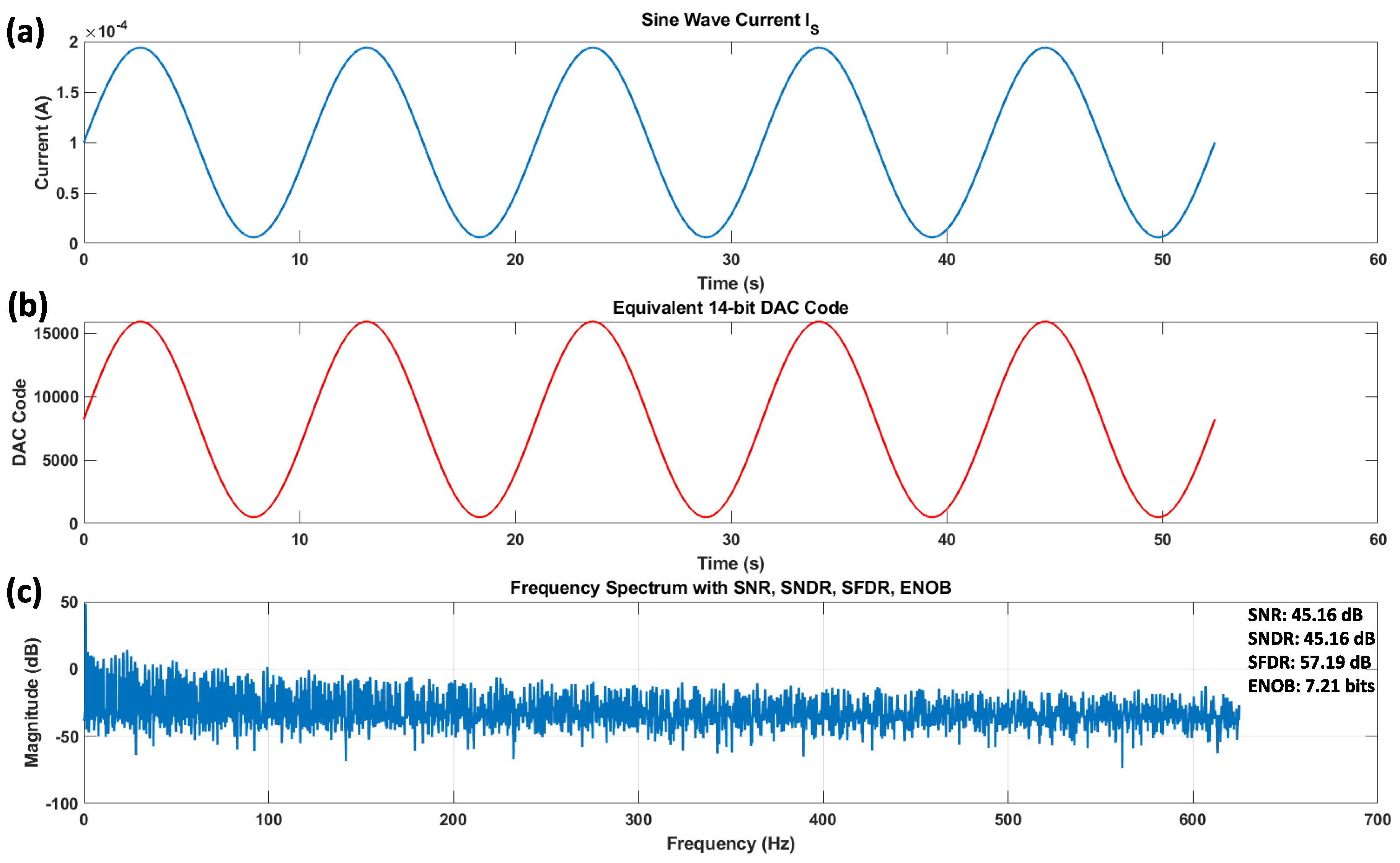

Table 1.
Current values and standard deviations for each bit at different temperatures ().
| Temp (°C) | Bit7 | Bit6 | Bit5 | Bit4 | Bit3 | Bit2 | Bit1 | Bit0 | Dummy | |
|---|---|---|---|---|---|---|---|---|---|---|
| -50 | mean | 1.00 | 0.50 | 0.25 | 0.13 | 0.0625 | 0.0312 | 0.0156 | 0.00777 | 0.00777 |
| std | 0.0138 | 0.00742 | 0.00402 | 0.00229 | 0.00141 | 0.000902 | 0.000611 | 0.000408 | 0.000408 | |
| 27 | mean | 1.00 | 0.50 | 0.25 | 0.13 | 0.0625 | 0.0312 | 0.0156 | 0.00778 | 0.00778 |
| std | 0.0108 | 0.00579 | 0.00313 | 0.00179 | 0.00111 | 0.000705 | 0.000477 | 0.000319 | 0.000319 | |
| 150 | mean | 1.00 | 0.50 | 0.25 | 0.13 | 0.0625 | 0.0312 | 0.0156 | 0.00778 | 0.00778 |
| std | 0.00814 | 0.00437 | 0.00235 | 0.00135 | 0.000836 | 0.000532 | 0.000360 | 0.000242 | 0.000242 |
Table 2.
Performance Summary and Comparison with other DxDCs.
| Items | This work | [15] | [16] |
|---|---|---|---|
| Process (nm) | 180 | 65 | 65 |
| Area (mm2) | 0.016 | 1.71 | 0.007 |
| Power (W) | 117 | 0.34 | 2250 |
| Energy/Conv. (pJ) | 1.52 | N.A. | 9 nJ |
| ENOB | 7.21 | N.A. | 10 |
| Inaccuracy | 0.36% | ±3.8% | 0.75% |
| Resolution () | 0.1375% | 2.4% | N.A. |
| Temperature(ºC) | -10 and 100 ºC | -20 to +80 | -55 to +200 |
| *Simulated in between -50 and 150 ºC | |||
Disclaimer/Publisher’s Note: The statements, opinions and data contained in all publications are solely those of the individual author(s) and contributor(s) and not of MDPI and/or the editor(s). MDPI and/or the editor(s) disclaim responsibility for any injury to people or property resulting from any ideas, methods, instructions or products referred to in the content. |
© 2024 by the authors. Licensee MDPI, Basel, Switzerland. This article is an open access article distributed under the terms and conditions of the Creative Commons Attribution (CC BY) license (https://creativecommons.org/licenses/by/4.0/).
Copyright: This open access article is published under a Creative Commons CC BY 4.0 license, which permit the free download, distribution, and reuse, provided that the author and preprint are cited in any reuse.


