
Submitted:
20 September 2024
Posted:
23 September 2024
You are already at the latest version
Abstract
Femtosecond laser two-photon polymerization (TPP) technology, known for its high precision and capability to fabricate arbitrary 3D structures, has been widely applied in the production of various micro-nano optical devices, achieving significant advancements particularly in the field of photonic wire bonding (PWB) for optical interconnects. Currently, research on optimizing both the optical loss and production reliability of polymeric photonic wires is still in its early stages. One of the key challenges is that inadequate metrology methods cannot meet the demand for multiphysical measurements in practical scenarios. This study utilizes in-situ scanning electron microscopy (SEM), for the first time, to monitor the working PWBs fabricated by TPP technology at the microscale. Optical and mechanical measurements are made simultaneously to evaluate the production qualities and to study the multiphysical coupling effects of PWBs. The results reveal that photonic wires with larger local curvature radii are more prone to plastic failure, while those with smaller local curvature radii recover elastically. Furthermore, larger cross-sectional dimensions contribute dominantly to the improved mechanical robustness. The optical loss deterioration of the elastically deformed photonic wire is only temporary, which can be fully recovered when the load is removed. After further optimization based on the results of multiphysical metrology, the PWBs fabricated in this work achieve a minimum insertion loss of 0.6 dB. In this study, the multiphysical analysis of PWBs carried out by in-situ SEM metrology offers a novel perspective for optimizing the design and performance of microscale polymeric waveguides, which could potentially promote the mass production reliability of TPP technology in the field of chip-level optical interconnection.
Keywords:
two-photon polymerization
; photonic wire bonding
; in-situ SEM
; optical loss
; mechanical reliability
1. Introduction
Femtosecond laser based two-photon polymerization (TPP) is an advanced technique that harnesses the ultra-short pulses and high peak power of femtosecond lasers to achieve 3D lithography in micro-nano scale [1,2,3,4]. Through two-photon absorption, it enables the precise construction of three-dimensional structures in photocurable resins [5,6]. This approach has been successfully employed in the fabrication of various micro-nano optical devices, which has promoted significant advancements in the field of chip-level optical interconnection [7,8,9]. For example, the TPP technology offers a novel solution for creating photonic wire bonds (PWB), enabling interconnections for chip-to-chip or chip-to-fiber scenarios [10,11,12]. Compared to optical coupling methods via precision alignment of microlenses, the advantages of PWB by TPP is significant. It bypasses the laborious mechanical alignment of precision optical elements between photonic chips, thereby improving overall chip yield. Additionally, PWB by TPP provides high production flexibility, making it adaptable to complicated optical configurations in the advanced scenarios of hybrid integration [13]. Most importantly, it facilitates automated large-scale production, paving the way for broader industrial applications.
As the fronts of photonic chip integrations continue to advance, there is an increasing demand for improved PWB performances, particularly regarding insertion loss due to reliability issues, which requires further validation by metrology methods. During fabrication, factors such as processing parameters, photoresist shrinkage, and development processes can compromise the dimensional accuracy of PWB microstructures [14,15]. Moreover, large overhang distances of PWBs weaken the mechanical stability of the structure and might induce unpredictable failures at working conditions. Without advanced metrology methods collecting multiphysical information at microscale, the optimization of PWBs regarding either optical loss or mechanical reliability is a black box problem. Meanwhile, existing testing methods are inadequate for real-time observation of deformation and optical loss in PWB under applied stress [16,17]. It is critical to enable the in-situ measurements of the optical loss and mechanical reliability of polymer waveguides like PWBs, so that the TPP production can eventually meet the high yield requirement of hybrid integrated photonic chip manufacturing.
With the development of three-dimensional manufacturing technologies at the micro- and nanoscale, in-situ scanning electron microscopy (SEM) is becoming an invaluable tool for the measurement and study of new materials and devices [18,19,20]. This method can simultaneously characterize both the mechanical properties and the microstructure of materials, significantly improving upon the "separated" and "static" limitations of traditional testing methods. Recently, in-situ SEM testing is evolving toward real-time and dynamic capabilities, allowing researchers to capture the key microstructural changes that dominantly influence the material properties [21,22,23]. This provides deeper insights into material behavior in practical applications. Researchers have utilized in-situ SEM to characterize the mechanical properties of TPP printed microstructures. For instance, R. Cherukuri et al. performed in-situ micropillar compression on SU-8 polymer fabricated via TPP, measuring mechanical properties such as modulus, hardness, yield strength, and strain rate sensitivity [24]. Similarly, N. Rohbeck et al. conducted a comprehensive study on the effects of temperature and strain rate on the mechanical properties of micron-sized 3D-printed polymers using Nanoscribe’s negative-tone photoresist IP-Dip [25]. Q. Li et al. employed in-situ SEM to measure the remarkable mechanical properties of Cu nanocluster-polymer micro-lattices [26], while Jens Bauer et al. characterized the compressive strength of micro-lattices and shell structures made from alumina-polymer composites [27]. However, there are currently few studies demonstrating the capability to measure both optical and mechanical properties, which is critically needed for the evaluation of PWBs. Specifically, when multiple physical fields are coupled (such as mechanical, thermal, and optical fields) upon microscale devices like PWBs in in-situ SEM testing, achieving a comprehensive and precise evaluation remains a significant technical challenge.
In this study, photonic wire bonds were fabricated using two-photon polymerization technology. Through simulation, the taper and bond dimensions were optimized, significantly reducing optical loss, with experimental results showing a minimum loss of 0.6 dB. A novel in-situ SEM metrology method is proposed, integrating optical coupling modules and nanomechanical measurements. The dynamic evolution of PWB microstructures is observed under SEM, while their optical and mechanical properties are measured simultaneously. The influences of cross-sectional size and curvature radius of the photonic wire on the mechanical robustness is examined. Good agreements are achieved with the numerical simulations. The real-time optical loss during deformation were collected to validate the multiphysical coupling in PWBs. The findings revealed that smaller local curvature radii of PWBs promise elastic recoveries over vertical indentations of 20 μm, which equals 15% of the photonic wire length. Larger cross-sectional sizes enhanced the load-bearing capacity of photonic wires. With properly selected local curvature radius and cross-sectional size, a fully recoverable PWB is demonstrated with both the geometrical shape and the optical loss to return to its initial value after the removal of force. This study pioneers the use of advanced in-situ metrology methods in promoting precise design and fabrication of TPP printed waveguides. The multiphysical results offer valuable insights for failure analysis and production optimization in advancing high-performance optical interconnect technologies. The combined methodology of microscale manufacturing and in-situ metrology establishes a strong foundation for further photonic device optimization.
2. Materials and Methods
2.1. Materials
The negative-tone photoresist (VancoreB) used for printing the photonic wire bonding (PWB) was purchased from Vanguard Corp. The single-mode fiber arrays with a mode field diameter of 10.4 μm used to accommodate interconnecting PWBs was purchased from FiberHom Incorporated.
2.2. PWB Fabrication and Characterization
Two-photon polymerization (TPP) was performed employing a Photonic Professional Sonata1000 (Vanguard) system. Microfabrication of all structures was performed in oil immersion mode with a femtosecond laser (780 nm, 100MHZ, 100fs) focused through a 40× oil objective lens (NA = 1.4; Zeiss). Printing was performed with a varied scan speed from 4 to 19 mm s−1 and laser power in the range of 2.89 to 5.78 mW. Slicing and hatching were set to 100 nm for all microgeometries. Fabricated structures on glass substrates were developed for 10 min in PGMEA, followed by rinsing with IPA for 5 min. The morphology of the fabricated structures from resists was observed using a Gemini SEM 360 scanning electron microscope (SEM, Zeiss). Prior to imaging, the structures were sputter coated with about 10 nm layer of Pt. The mechanical properties of the PWBs were tested via the in situ quantitative PicoFemto (NI-100) equipped with a 100 μm customized tungsten carbide cylindrical indenter with a speed of 200 nm s−1 inside the SEM. In the optical loss testing of the PWB, a single-frequency light source with a working wavelength of 1550 nm (ZG-T-15-100-SM, Hunyuan Technology Co., Ltd.) was applied to one side of the fiber array. A storage-type optical fiber power meter (MT-7603-C, Pro'sKit) was connected to the other end. The inherent loss of each channel was specified before the FA samples were shipped. To accurately determine the actual optical loss of the PWB, the loss from the fiber array must be excluded.
2.3. FEM Simulation
The optical simulations were performed using Lumerical software, with a PWB refractive index of n=1.53 and air (n = 1) as the surrounding medium. A laser source with a wavelength of 1550 nm was used, and the fiber dimensions and refractive index were based on FiberHome@SMF-G657A1 optical fiber specifications. The mechanical reliability simulation of PWB was performed using Abaqus software. The static analysis was used to simulate the compression process due to the low loading speed. The contact algorithm was configured as “general contact”, allowing all surfaces to interact realistically. Additionally, the tangential friction coefficient was set to 0.1, and the expected contact behavior was defined as hard contact to better reflect actual conditions. The photoresist material has a Poisson’s ratio v = 0.49, with a Young’s modulus of 2.0 GPa and a yield stress of 0.07 GPa. The eight-node linear brick element (C3D8R) is used for linear-elastic analysis.
3. Results and Discussion
3.1. In-Situ Multiphysical Metrology
A novel set of metrology methods for PWBs is designed based on the existing in-situ SEM nanomechanical measurement platform, allowing simultaneous capturing of micro-nano scale morphological changes during mechanical loading and optical loss monitoring. The nanomechanical measurement enables the quantitative evaluation of the mechanical reliability of PWB, while the simultaneous optical loss monitoring establishes correspondence between mechanical perturbation and waveguide performance. The schematic diagram and SEM snapshots of the measurement process is shown in Figure 1. The two fiber arrays (FAs) with printed interconnecting PWBs are placed on a three-axis piezo stage of the nanomechanical tester beneath a specially shaped indenter with a force sensor. The indenter is designed and milled in a focused ion beam (FIB) SEM to avoid disruptive loading on the curved photonic wires (Figure S1). As the optical measurement module, both ends of the two FAs are connected to optical fibers outside the SEM chamber through the flange on the chamber wall. One fiber is connected to an external laser of the wavelength of 1550 nm; and the other fiber is connected to a laser power meter. The total optical loss is then calculated to be the ratio of the reading of the power meter over the input power from the laser. In a typical mechanical test with optical loss monitoring, the indenter is driven by displacement control and apply contact pressure on the highest location of the photonic wire. At the same time, SEM imaging is conducted at video rate for a clear observation of deformation, while the laser power meter reading is collected for optical loss calculation under varying mechanical loads. Overall, this in-situ SEM measurement method captures real-time microscale deformations of working polymeric waveguides, such as PWBs, and correlates stress-strain responses with optical loss data, offering a comprehensive and detailed insights into the multiphysical behavior of PWBs.
3.2. Laser Parameters of PWB by TPP.
The femtosecond laser exposure in the process of TPP is crucial to obtain prints with good surface qualities. High surface qualities of polymeric waveguides like PWBs then guarantee the desirable optical transmission functions. Therefore, the optimized laser exposure parameters during TPP process are determined through surface quality examinations of PWBs based on SEM observations. In principle, reduced laser exposure leads to a lower extent of crosslinking of resins and polymeric network formation, which results in either incomplete curing of the intended structure or no curing at all, as show in Figure S2. As the laser exposure increases, the crosslinking extent also increases, while the accumulation of heat could jeopardize the printing by bringing shape distortions or bubble formations. As shown in Figure 2a,b, at relatively low laser powers, the surface of the photonic wires are filled with nanometer level steps, that is, a typical sign of poor quality TPP printing. When the laser power is elevated to 4.80 mW, freestanding photonic wires with smooth surfaces are fabricated (Figure 2c). As the laser power is further increased to 5.78 mW, overexposure is clearly observed, causing the cylindrical photonic wire to become irregularly thickened (Figure 2d). Similarly, the effect of laser scanning speed on the printed quality of PWB is also explored and optimized, as shown in the Figure S3. As a result, for the TPP experiment in this work, a printing speed of 16 mm/s and a laser power of 4.8 mW are used to fabricate PWBs with uniform diameters and excellent surface quality.
3.3. Geometrical Design for Low-Loss PWB
The optical loss of the PWB directly indicates its optical transmission efficiency. To minimize interconnection losses, the two ends of the PWB must be precisely spatially aligned with the connected photonic components. Firstly, the PWB’s cross-section should match the optical mode diameter of the interconnecting components to ensure optimal photonic signal transmission. Then, the PWB's trajectory should be carefully planned to avoid optical losses due to sharp bends. These two factors represent the biggest challenge in the PWB design. In our work, to ensure mode matching with the optical fiber port, the ends of the PWB are designed with a tapered structure to facilitate efficient optical signal transmission. In a taper with a circular cross-section, the diameter decreases linearly from w2 to w1 over the taper length (Ltaper), with the tail end matching the diameter of the bond, both being w1, as shown in Figure 3a. The bond size determines the light propagation mode in the PWB. For small waveguide diameters, a single mode dominates, characterized by a simpler structure with the electromagnetic field concentrated at the waveguide's center. As the diameter increases, higher-order modes begin to appear, leading to increased optical losses. Figure 3b illustrates simulations of the electric field modes for circular waveguides with varying cross-sectional diameters using the FDE method. Enlarging the bond diameter alters the optical field's mode distribution, reducing the normalized field intensity at the waveguide interface and diminishing interaction with the sidewall, which decreases transmission losses [28]. By optimizing the waveguide diameter, low-loss optical transmission can be achieved within a specific frequency range, thereby enhancing waveguide performance. FDE simulations were also used to calculate the overlap integral between the PWB mode and the single-mode fiber, estimating the optical loss for tapers with different widths (w2). As shown in Figure 3c, as the w2 size increases, the optical loss decreases to a certain point and then increases. When the fiber diameter reaches 14μm, the loss reaches its minimum. Additionally, the insertion loss at the interface between the PWB and fiber for different taper lengths was simulated, as shown in Figure 3d. A circular taper cross-section was used, and the insertion loss was optimized by adjusting the taper length. The circular taper cross-section was chosen because it provides better optical transmission efficiency and lower insertion loss. Simulations using the FDTD (Finite Difference Time Domain) method were conducted for different taper lengths, with fixed values of w1 = 3 μm and w2 = 14 μm, showing that the loss stabilized when the length reached around 75 μm. Optical losses for different PWB curvature radii were also simulated and analyzed. As shown in Figure 3e, when w1 is fixed at 3 μm, smaller waveguide curvature radii lead to higher optical loss. This is because smaller curvature radii cause more bending and scattering of light within the waveguide, increasing transmission loss. As the curvature radii increases, optical loss gradually decreases. When the waveguide curvature radii reach approximately 30 μm, the loss stabilizes, and further increases in curvature radii have little effect. This indicates that once the waveguide curvature radii exceed a certain threshold, the light’s transmission path becomes smoother, and loss is primarily determined by material absorption and scattering. Overall, in the PWB design, both taper length and bond curvature radii can heavily impact the optical loss. In this work, with the FA-FA distance fixed at 280 μm, a taper length of 75 μm and a bond overhang of 130 μm are selected as the optimized design. The local curvature radii of the bond are restricted to 30 μm or larger. After optimization, the PWB was successfully printed, and optical loss testing results are shown in Figure 3f. The experiment measured the total optical loss of the fiber array and the PWB, as well as the loss of the fiber array itself, revealing that the insertion loss of the PWB remained below 3 dB, with a minimum of 0.6 dB. The results demonstrate that optimized design and precise printing significantly reduce coupling loss, thereby improving the overall optical transmission performance of the system.
3.4. Mechanical Resilience and Optical Recovery of PWB
The mechanical resilience of PWBs is a crucial but often neglected evaluation for the reliable TPP production of high-precision chip-level photonic interconnects. In a typical PWB fabrication process, TPP is followed by processes such as development in solvents, multiple rinsing procedures and cladding by low refractive index resins, which are not as precisely controllable as the high-resolution TPP printing. To ensure that PWBs maintain the structural integrity through these additional processes, a certain level of mechanical resilience is apparently needed. For example, isopropyl alcohol (IPA) is a regularly used solvent in the rinsing process of TPP, which has a surface tension of 22 mN/m [29]. For a PWB across the distance of 280 μm, the maximum capillary force suffered by the PWB structure during the drying of IPA would be around 12 μN. In another word, it should be ensured that the PWB structure can elastically recover from such external loads, so that the optimized optical transmission can be retained in the end.
Therefore, the impact of geometrical parameters of PWBs on the mechanical resilience are examined with in-situ SEM measurements. PWBs with different curvature radii were tested to observe their deformation under specific compression. When the curvature radius was 50 μm, the PWB failed to recover after a 20 μm compression, exhibiting plastic deformation, as shown in Figure 4a. In contrast, with radii of 40 μm and 30 μm, the PWBs fully recovered, displaying elastic deformation, as shown in Figure 4b,c. These results indicate that PWBs with larger curvature radii have lower elastic displacement capacity in the vertical direction and are more prone to permanent deformation, and vice versa. Figure 4d,e show the experimental and numerically simulated force-displacement curves for PWBs with different curvatures, respectively. The resemblance of compression and recovery behaviors indicates a mutual validation between experimental and simulated data. The in-situ multiphysical measurement used in this work allows simultaneous monitoring of optical loss during the compression and recovery of PWB. As seen in Figure 4f, during compression, optical loss increases proportionally with the indentation displacement. Once the indenter is retracted, causing the PWB structure to recover to its initial shape, the optical loss also returns to its initial value. This is the direct evidence that the elastic recovery of the PWB can guarantee preserved optical transmission with no accumulation effects on the losses. It is worth noting that the platinum coating for SEM observation, despite causing a higher initial optical loss, does not affect the full optical recovery while mechanically fatigued along with the PWB.
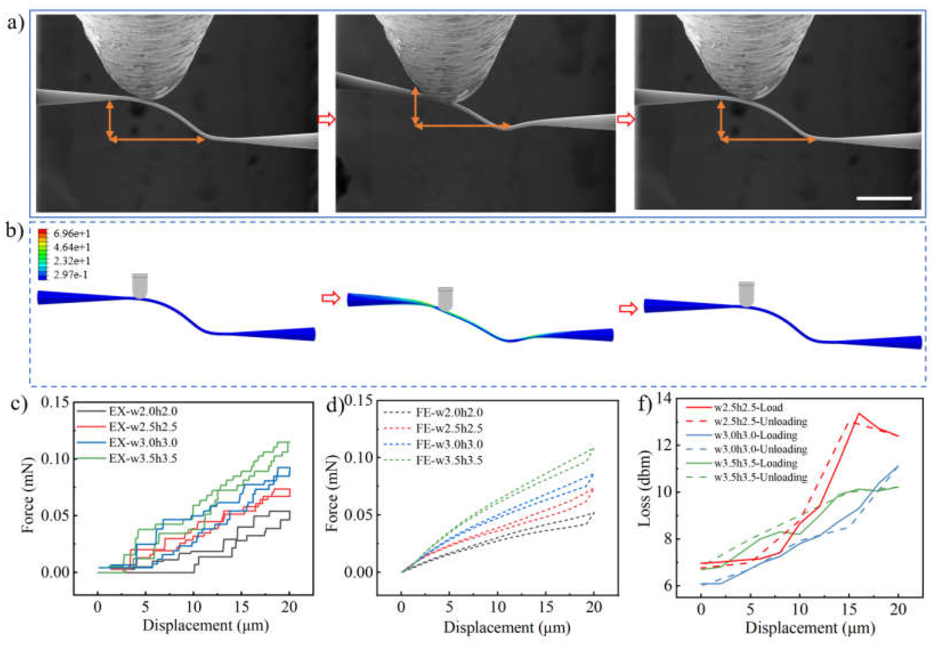
To further explore the variation in PWB mechanical resilience with changes in bond cross-sectional size, the cross-sectional size of the bond was altered while keeping all other PWB dimensions constant. Figure 5a shows the SEM images of the PWB with a bond diameter of 3 μm before and after a 20 μm compression. It is clearly observed that the PWB undergoes significant deformation during the compression process, but it fully recovers once the indenter is removed, indicating that elastic deformation has occurred. Figure 5b presents the simulation results of the PWB during compression, where stress is primarily concentrated on the upper and lower surfaces of the bond and at the junction with the taper. Figure 5c,d show the force-displacement curves obtained from the experiments and simulations, respectively, which are in good agreement. Additionally, the compressive strength of the PWB increases as the bond size increases. During the compression of PWB, its optical loss was also measured, as shown in Figure 5f. As the compression increased, the deformation of the PWB, leading to a corresponding rise in optical loss. However, once the indenter was lifted and the PWB recovered its original shape, the optical loss was able to return to its initial value.
4. Conclusions
Here, in order to achieve the goal of measuring multiphysical responses of photonic wire bonding (PWB) fabricated by two-photon polymerization (TPP), a novel in-situ SEM technique, integrating optical and nanomechanical measurements, is developed. With the help of real-time observations on PWB morphological changes, concurrently analysis is conducted on the relationship between the force-displacement curve and optical loss. The optimal printing process is identified. The optical loss of the PWB is ultimately reduced to as low as 0.6 dB. The mechanical resilience and optical recovery of the PWB are also investigated. It is observed that when the PWB curvature radius is reduced to below 40 μm, the photonic wire is able to fully recover, evading undesired plastic deformation. Further analysis reveals that the mechanical resilience of the PWB increases with bond cross-sectional size (from 2 to 3.5 μm), which guarantees a necessary load-bearing capacity. Within the elastic deformation range, optical loss of the PWB increases under loading but returns to its initial value once the load is retracted. These detailed studies on the relationship between the mechanical reliability and optical transmission of PWBs facilitate the optimization of design and process parameters, leading to new industrial prospects where advanced metrology methods boost the knowledge and eventually the yield of micro-nano scale chip-level manufacturing.
Supplementary Materials
The following supporting information can be downloaded at the website of this paper posted on Preprints.org, Figure S1: SEM image of in-situ indenter; Figure S2: SEM image of failed print of photonic wire bonds; Figure S3: SEM images of PWB at increasing laser speed.
Author Contributions
Conceptualization, B.D. and R.X.; methodology, Y.L. and X.H.; software, W.S.; and Y.W.; validation, Y.L., and W.S.; formal analysis, B.D.; data curation, Y.L., and W.S.; writing—original draft preparation, Y.L.; writing—review and editing, J.G and B.D.; project administration, B.D. and X.L.; funding acquisition, R.X., B.D. and Y.L. All authors have read and agreed to the published version of the manuscript.
Funding
This work was funded by National Key Research and Development Program of China Grant 2023YFB2806400; Zhejiang Provincial Natural Science Foundation of China Grant LQ24F050017; Yongjiang Laboratory Grant B400EASE02.
References
- Florea, L.; Blasco, E.; Mattoli, V. , New Frontiers in Materials and Technologies for 3D Two Photon Polymerization. Advanced Functional Materials 2023, 33(39), 2305697. [Google Scholar] [CrossRef]
- Schwärzle, D.; Hou, X.; Prucker, O.; Rühe, J. , Polymer Microstructures through Two-Photon Crosslinking. Advanced Materials 2017, 29(39), 1703469. [Google Scholar] [CrossRef] [PubMed]
- Bauer, J.; Guell Izard, A.; Zhang, Y.; Baldacchini, T.; Valdevit, L. , Programmable Mechanical Properties of Two-Photon Polymerized Materials: From Nanowires to Bulk. Advanced Materials Technologies 2019, 4(9), 1900146. [Google Scholar] [CrossRef]
- Chu, W.; Tan, Y.; Wang, P.; Xu, J.; Li, W.; Qi, J.; Cheng, Y. , Centimeter-Height 3D Printing with Femtosecond Laser Two-Photon Polymerization. Advanced Materials Technologies 2018, 3(5), 1700396. [Google Scholar] [CrossRef]
- Henning, I.; Woodward, A. W.; Rance, G. A.; Paul, B. T.; Wildman, R. D.; Irvine, D. J.; Moore, J. C. , A Click Chemistry Strategy for the Synthesis of Efficient Photoinitiators for Two-Photon Polymerization. Advanced Functional Materials 2020, 30(50), 2006108. [Google Scholar] [CrossRef]
- Han, F.; Gu, S.; Klimas, A.; Zhao, N.; Zhao, Y.; Chen, S.-C. , Three-dimensional nanofabrication via ultrafast laser patterning and kinetically regulated material assembly. Science 2022, 378(6626), 1325–1331. [Google Scholar] [CrossRef]
- Burmeister, F.; Zeitner, U. D.; Nolte, S.; Tünnermann, A. , High numerical aperture hybrid optics for two-photon polymerization. Opt. Express 2012, 20(7), 7994–8005. [Google Scholar] [CrossRef]
- Pudis, D.; Goraus, M.; Urbancova, P. , Optical properties of woodpile structures for application on the surface of photonic devices. Applied Surface Science 2018, 461, 227–232. [Google Scholar] [CrossRef]
- Yao, P.; Liu, R.; Broggini, T.; Thunemann, M.; Kleinfeld, D. , Construction and use of an adaptive optics two-photon microscope with direct wavefront sensing. Nature Protocols 2023, 18(12), 3732–3766. [Google Scholar] [CrossRef]
- Billah, M. R.; Blaicher, M.; Hoose, T.; Dietrich, P.-I.; Marin-Palomo, P.; Lindenmann, N.; Nesic, A.; Hofmann, A.; Troppenz, U.; Moehrle, M.; Randel, S.; Freude, W.; Koos, C. J. O. , Hybrid integration of silicon photonics circuits and InP lasers by photonic wire bonding. Optica 2018, 5(7), 876–883. [Google Scholar] [CrossRef]
- Lin, B.; Witt, D.; Young, J. F.; Chrostowski, L. , Cryogenic optical packaging using photonic wire bonds. APL Photonics 2023, 8(12), 126109. [Google Scholar] [CrossRef]
- Cai, C.; Wang, J. , Femtosecond Laser-Fabricated Photonic Chips for Optical Communications: A Review. Micromachines 2022, 13, 630. [Google Scholar] [CrossRef] [PubMed]
- Juodkazis, S., Laser polymerized photonic wire bonds approach 1 Tbit/s data rates. Light: Science & Applications 2020, 9 (1), 72.
- Blaicher, M.; Billah, M. R.; Kemal, J.; Hoose, T.; Marin-Palomo, P.; Hofmann, A.; Kutuvantavida, Y.; Kieninger, C.; Dietrich, P.-I.; Lauermann, M.; Wolf, S.; Troppenz, U.; Moehrle, M.; Merget, F.; Skacel, S.; Witzens, J.; Randel, S.; Freude, W.; Koos, C., Hybrid multi-chip assembly of optical communication engines by in situ 3D nano-lithography. Light: Science & Applications 2020, 9 (1), 71.
- Kiefer, P.; Hahn, V.; Nardi, M.; Yang, L.; Blasco, E.; Barner-Kowollik, C.; Wegener, M. , Sensitive Photoresists for Rapid Multiphoton 3D Laser Micro- and Nanoprinting. Advanced Optical Materials 2020, 8(19), 2000895. [Google Scholar] [CrossRef]
- Lindenmann, N.; Balthasar, G.; Hillerkuss, D.; Schmogrow, R.; Jordan, M.; Leuthold, J.; Freude, W.; Koos, C. , Photonic wire bonding: a novel concept for chip-scale interconnects. Opt. Express 2012, 20(16), 17667–17677. [Google Scholar] [CrossRef]
- Gu, Z.; Amemiya, T.; Ishikawa, A.; Atsumi, Y.; Arai, S. J. J. o. L. M. , Investigation of Optical Interconnection by using Photonic Wire Bonding. Journal of Laser Micro 2014, 10(2), 148–153. [Google Scholar] [CrossRef]
- Liang, Y.; Luo, A.; Wang, L.; Hu, S.; Guo, W.; Yao, Y.; Wan, Q. , In-situ SEM investigation of low-cycle fatigue behavior and microstructure evolution of CoCrNi medium entropy alloy. Journal of Materials Research and Technology 2023, 25, 1–12. [Google Scholar] [CrossRef]
- Barrios, A.; Kunka, C.; Nogan, J.; Hattar, K.; Boyce, B. L. , Automated High-Throughput Fatigue Testing of Freestanding Thin Films. Small Methods 2023, 7(7), 2201591. [Google Scholar] [CrossRef]
- Wang, X.; Zhao, Y.; Wang, L.; Wei, L.; He, J.; Guan, X. , In-situ SEM investigation and modeling of small crack growth behavior of additively manufactured titanium alloy. International Journal of Fatigue 2021, 149, 106303. [Google Scholar] [CrossRef]
- Juri, A. Z.; Basak, A. K.; Yin, L. , In-situ SEM micropillar compression of porous and dense zirconia materials. Journal of the Mechanical Behavior of Biomedical Materials 2022, 132, 105268. [Google Scholar] [CrossRef]
- Chen, B.; Yang, R.; Dong, J.; Wang, S.; Wang, J.; Huan, Y. , Development of in-situ SEM torsion tester for microscale materials. Measurement 2019, 139, 421–425. [Google Scholar] [CrossRef]
- Fritz, R.; Kiener, D. , Development and application of a heated in-situ SEM micro-testing device. Measurement 2017, 110, 356–366. [Google Scholar] [CrossRef]
- Cherukuri, R.; Lambai, A.; Sukki, L.; Väliaho, J.; Kallio, P.; Sarlin, E.; Ramachandramoorthy, R.; Kanerva, M.; Mohanty, G. , In-situ SEM micropillar compression and nanoindentation testing of SU-8 polymer up to 1000 s−1 strain rate. Materials Letters 2024, 358, 135824. [Google Scholar] [CrossRef]
- Rohbeck, N.; Ramachandramoorthy, R.; Casari, D.; Schürch, P.; Edwards, T. E. J.; Schilinsky, L.; Philippe, L.; Schwiedrzik, J.; Michler, J. , Effect of high strain rates and temperature on the micromechanical properties of 3D-printed polymer structures made by two-photon lithography. Materials & Design 2020, 195, 108977. [Google Scholar]
- Li, Q.; Kulikowski, J.; Doan, D.; Tertuliano, O. A.; Zeman, C. J.; Wang, M. M.; Schatz, G. C.; Gu, X. W. J. S., Mechanical nanolattices printed using nanocluster-based photoresists. Science (New York, N.Y.) 2022, 378 (6621), 768-773.
- Bauer, J.; Schroer, A.; Schwaiger, R.; Kraft, O. , Approaching theoretical strength in glassy carbon nanolattices. Nature Materials 2016, 15(4), 438–443. [Google Scholar] [CrossRef] [PubMed]
- Vlasov, Y. A.; McNab, S. J. , Losses in single-mode silicon-on-insulator strip waveguides and bends. Opt. Express 2004, 12(8), 1622–1631. [Google Scholar] [CrossRef]
- Park, J.-G.; Lee, S.-H.; Ryu, J.-S.; Hong, Y.-K.; Kim, T.-G.; Busnaina, A. , Interfacial and Electrokinetic Characterization of IPA Solutions Related to Semiconductor Wafer Drying and Cleaning. Journal of The Electrochemical Society 2006, 153(9), G811–G814. [Google Scholar] [CrossRef]
Figure 1.
Measurement of optical loss and mechanical properties of PWBs using in-situ SEM.
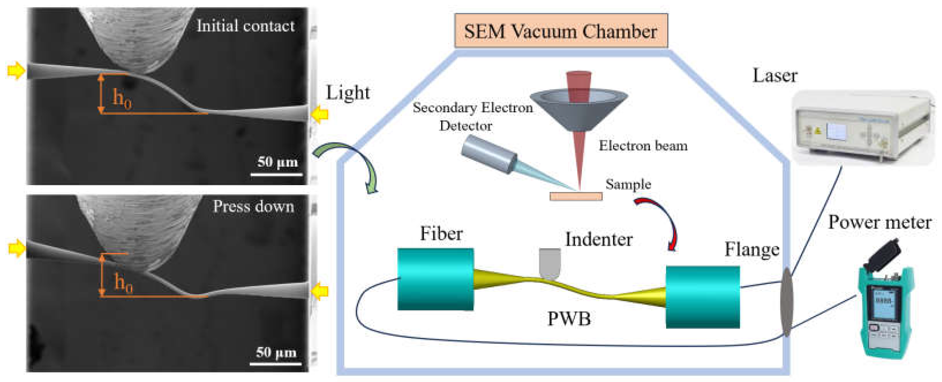
Figure 2.
SEM images of PWBs at increasing TPP process laser powers, Scale bars: 5 μm.
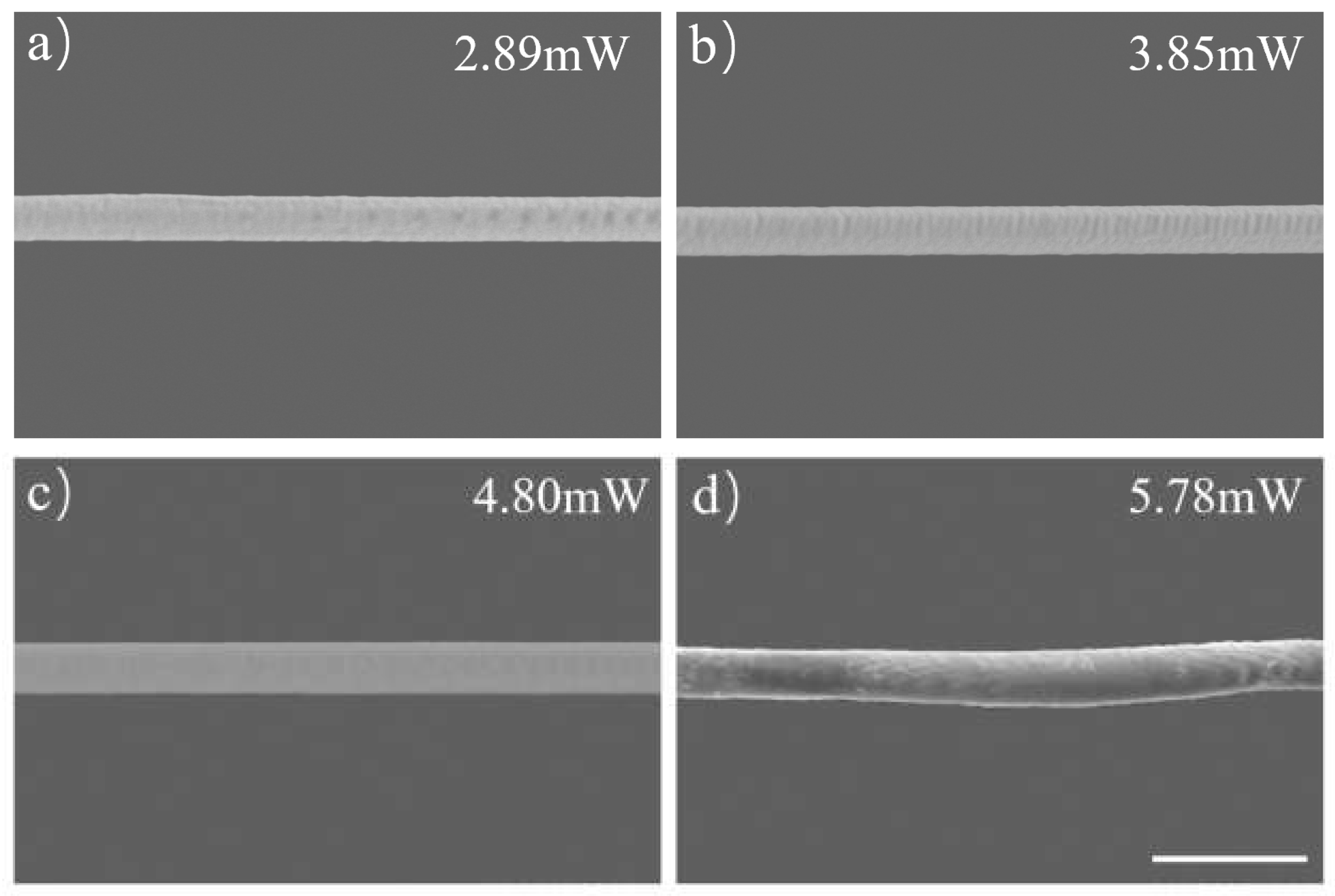
Figure 3.
shows the optical loss measurements of the PWB. (a) provides a schematic of the photonic wire bond design parameters, highlighting the significant difference between the mode field diameters of a standard single-mode fiber (FiberHome@SMF-G657A1) and the PWB. The typical mode field diameter of an SMF is 10.4 μm, while that of the PWB is less than 3 μm. Simulations were conducted to evaluate optical loss for varying bond cross-sectional diameters (w1) (b), taper widths (w2) (c), taper lengths (Ltaper), and bond curvature radius (R) (e). (f) presents the measured optical losses of printed PWB structures with varying bond cross-sectional diameters in an FA-FA array with a total length of 280 μm, while maintaining fixed parameters of w2 = 14 μm, Ltaper = 75 μm, and a curvature radius of R = 40 μm.
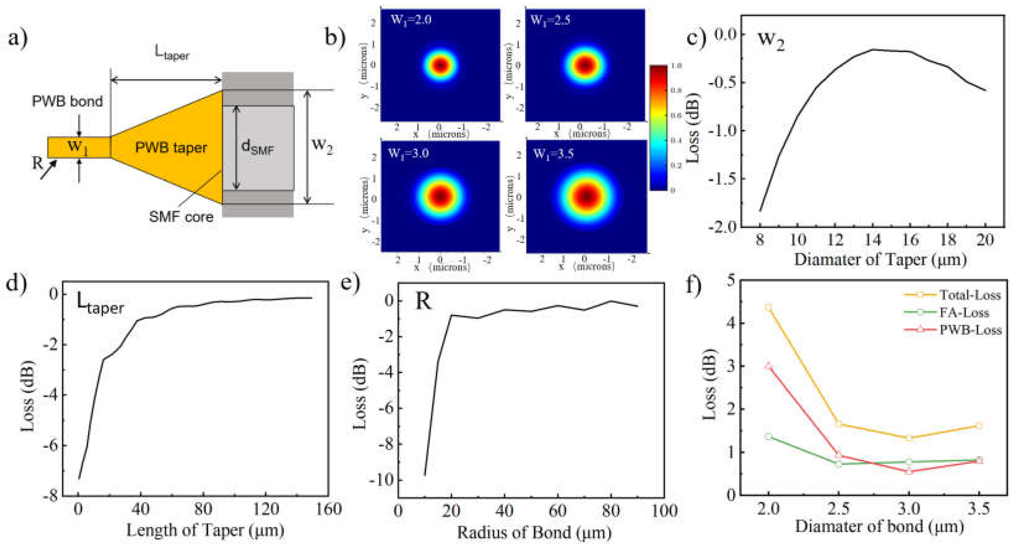
Figure 4.
Compression experiments on PWBs with different curvature radius. (a) SEM images of the PWB during compression with curvature radius of 50 μm (a), 40 μm (b), and 30 μm (c). (d) and (e) Force-displacement curves of the PWB under experimental and simulation conditions. (f) Optical loss corresponding to the PWB during the compression process. Scale bars: 40 μm.
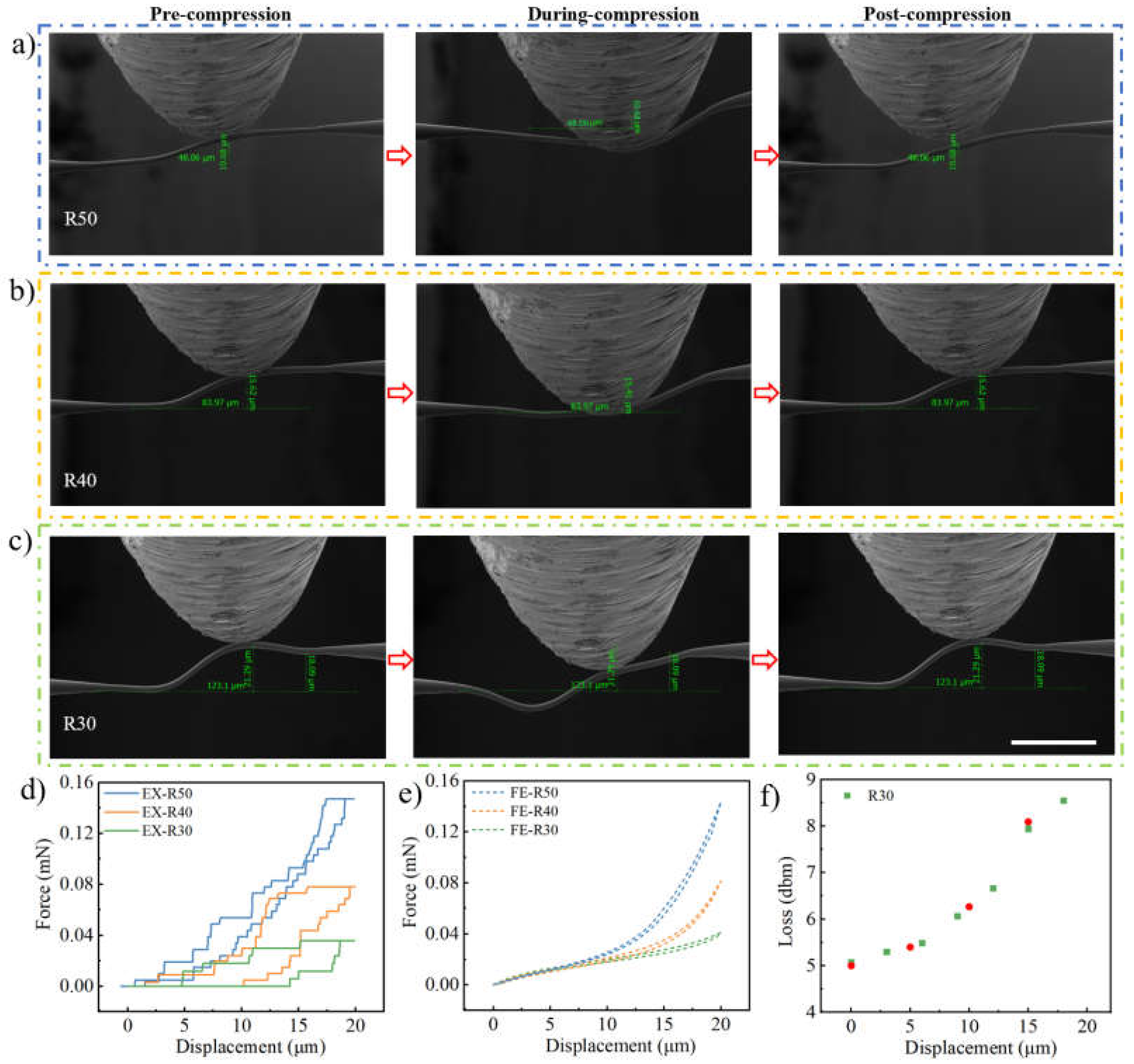
Figure 5.
Compression experiments on PWBs with different bond diameters. (a) SEM image show the deformation process of PWB during the compression process; The PWB with a curvature radius of 30 μm exhibits reversible deformation when compressed by 20 μm; (b) Finite element simulations of the compression response of the PWB structure in Figure (a); (c) and (d) The force–displacement curve of PWB of under experimental and simulation conditions; (f) The optical loss corresponding to PWB during the compression process; Scale bars: 40 μm.
Disclaimer/Publisher’s Note: The statements, opinions and data contained in all publications are solely those of the individual author(s) and contributor(s) and not of MDPI and/or the editor(s). MDPI and/or the editor(s) disclaim responsibility for any injury to people or property resulting from any ideas, methods, instructions or products referred to in the content. |
© 2024 by the authors. Licensee MDPI, Basel, Switzerland. This article is an open access article distributed under the terms and conditions of the Creative Commons Attribution (CC BY) license (http://creativecommons.org/licenses/by/4.0/).
Copyright: This open access article is published under a Creative Commons CC BY 4.0 license, which permit the free download, distribution, and reuse, provided that the author and preprint are cited in any reuse.


