
Submitted:
22 September 2024
Posted:
24 September 2024
You are already at the latest version
Abstract
— An extreme bandgap Al0.64Ga0.36N quantum channel HEMT with Al0.87Ga0.13N top and back barriers grown by MOCVD over bulk AlN substrate demonstrated a critical breakdown field of 11.37 MV/cm, higher than 9.8 MV/cm expected for the channel Al0.64Ga0.36N material. We show that the fraction of this increase is due to the quantization of the 2D electron gas. The polarization field maintains electron quantization in the quantum channel even at low sheet densities in contrast to conventional HEMT designs. An additional increase in the breakdown field is due to quantum-enabled real space transfer of energetic electrons into high-Al barrier layers in high electric fields. These results show the advantages of quantum channel design for achieving record high breakdown voltages and enabling superior power HEMT devices.
Keywords:
HEMT
; AlGaN
; quantization
; breakdown field
; mobility
1. Introduction
Ever since their emergence in the early 1990s [1,2] GaN High Electron Mobility Transistors have demonstrated superior performance for high voltage [3,4], high frequency [5,6], high temperature [7,8] operation, and excellent radiation hard potential [9,10]. The prime reasons for their superiority for operation in extreme environments are a wide energy gap leading to a high breakdown voltage and polarization doping [11,12] supporting large sheet electron densities in the HEMT channels. A high polar optical phonon energy in GaN (91.2 meV [13] compared to 35 meV for GaAs [14]) and screening of impurity scattering by a large electron density in the device channel ensure a high field effect mobility, especially in the on state, and lead to a low on-resistance for long [15,16,17] and short channel devices.[18]. In this paper, we show that these advantages could be dramatically enhanced using the Quantum Channel HEMT (QC-HEMT) design. QC-HEMT incorporates a thin channel comparable sandwiched between the top and bottom wide bandgap barriers. Figure 1 compares conventional HEMT and QC-HEMT designs.
In contrast to conventional GaN HEMT designs, the shape of the potential confining two-dimensional electron gas (2DEG) in QC-HEMT is determined by both the polarization field and bandgap discontinuities at the top and bottom barrier interface. Carrier confinement in the HEMT 2D electron gas (2DEG) channel affects most device performance parameters. Strong electron confinement reduces trapping and related gate- and drain lags, increases channel mobility, and helps achieve lower contact resistance. However, in conventional single heterojunction HEMTs, band diagrams flatten out at gate voltages close or below the threshold reducing or eliminating electron confinement. As we show in this work, in addition to maintaining confinement, the quantization of 2DEG in the QC design enables the effect that we call quantum real space transfer (QRST). QRST leads to achieving breakdown fields exceeding those predicted by the material properties of the device channel.
The QC HEMT advantages could be greatly enhanced using Extreme bandgap (EBG) semiconductors with bandgap energy exceeding 4 – 5 eV, such as AlGaN with Al-fraction x>0.6. These devices show strong promise for achieving record high breakdown voltage, high-temperature operation, radiation hardness, and chemical stability [19,20,21]
For high-power III-Nitride EBG devices, the choice of substrate has critical importance. Substrate lattice matching to device active layers is needed to avoid strain relaxation and defect generation. Bulk AlN is thus the best choice of substrate for high-Al AlGaN devices[22], and we employ it in our design. Bulk AlN substrate [23] also has high thermal conductivity to provide efficient thermal management of high-power devices.
2. QC-HEMT Design and Key Properties
2.1. Energy States and Band Diagram
QC HEMT design leads to two important results: first, the two-dimensional electron gas in the device channel is confined at gate voltages close to or even slightly below the threshold and second, the ground state in the quantum well remains well above the bottom of the conduction band in GaN. The ground state energy can be estimated as [24]
where nq is the quantum number (nq = 0 for the ground state), and Feff is the effective electric field in the channel. Our simulations show that, just like for Si MOSFETs [25], the effective electric field in the conventional HEMT is approximately
Here Fi is the electric field at the barrier-channel interface, ns is the sheet electron density in the channel, εo is the dielectric permittivity of vacuum, and ε =8.9 is the GaN dielectric constant. Factor 2 in the denominator accounts for the band bending
For the QC HEMT , where Fs is the polarization field that depends on the molar fractions of the cladding layers and the QC thickness. We used a self-consistent solution of the Schrodinger-Poisson equation to estimate Fs = 108 V/m. We have also found the ground energy states for QC HEMT using a 1D Poisson simulator by G. Shnider [26] and obtained very close results.
Figure 2 shows the energy band diagram of the QC-HEMT with a channel thickness of 2 nm.
Figure 3 compares the dependencies of the ground state energy E0 above the bottom of the conduction band on the sheet carrier concentration ns for the regular HEMT and for the QC HEMT with a 2 nm thick channel generated using Eqs. (1-3).
As seen, in conventional HEMT at gate voltage close to the threshold, (nS => 0), the ground state energy practically coincides with the bottom of conduction band Ec. In contrast, in QC-HEMT, the ground state energy remains well above Ec in a broad range of 2DEG densities. This QC-HEMT feature makes an important impact on the device breakdown field.
- A.
- Breakdown field in QC-HEMT
As seen, the position of the lowest quantum state E0 in the quantum channel device remains practically constant even at ns at the gate voltage close to the threshold. This is equivalent to the effective increase in the energy gap by E0. Note that for the breakdown field consideration, the device parameters at the gate voltage close to the threshold are particularly important. The analysis presented in reference [27] shows that the breakdown field, FBR, is approximately proportional to EG2.5, consistent with the experimental data presented in [28]. For QC-HEMT, the effective energy gap EGeff = EG + E0. For the QC-HEMT of Figure 2, EG =3.39 eV, E0=0.45 eV at gate voltage close to the threshold, and the resulting increase in an FBR is around 36%.
Strong electron confinement in QC-HEMT may lead to another important effect resulting in further FBR increase. As shown in [29] at high electron energies, real space transfer of hot electrons from the quantum well into the barrier should occur. Figure 4 shows the simulated electron wave function for the QC HEMT of Figure 2. As seen, strong electron confinement leads to a significant fraction of electrons penetrating the top barrier.
Therefore, it is reasonable to expect that at a high electric field, a large fraction of the channel would experience quantum transfer to the top barrier. Since the top barrier is made of material with a larger bandgap (in our example, it is AlGaN with 65% Al), a further significant increase in the effective breakdown field FBR is expected. This effect requires further theoretical and experimental studies.
- B.
- Electron mobility in QC-HEMT
Strong electric confinement in QC HEMT leads to a smaller 2DEG effective Δd thickness than it is for a conventional HEMT. The Δd could be estimated as the ratio of the ground state energy over the electric field at the heterointerface:
Hence, bulk (volume) electron density for the same ns value is higher in QC HEMT as compared to conventional HEMT. Figure 5 shows the volume electron density as a function of ns in conventional and QC HEMT calculated using Eqs. (1 – 3).
As seen, for conventional HEMT, volume electron density rapidly decreases as ns decreases, i.e., as the gate bias approaches the threshold because the effective width of the 2DEG Δd in conventional HEMT rapidly increases as the gate bias approaches the threshold; 2DEG confinement nearly disappears. In QC HEMT, the volume electron density is a much slower function of ns. A relative increase in volume density leads to better screening and less impurity scattering, hence to higher mobility. Figure 6a illustrates this expected improvement extracted from the measured data [30]. Experimental confirmation of mobility increase due to better confinement in double heterostructure (DH) HEMTs has been obtained earlier in [31]. This data is shown in Figure 6(b). The field effect mobility in III-Nitride HEMTs depends on many factors such as interface roughness, defect concentration, strain, alloy scattering, and dislocation density. However, strong scattering screening due to higher concentration should result in higher mobility in any HEMT. QC HEMT with a 2 nm thick channel exhibits nearly 10 times higher electron confinement than in the DH HEMT reported in [31].
2. Experimental Validation of QC HEMT Breakdown Field Enhancement
2.1. Device Fabrication
Pseudomorphic Al0.87Ga0.13N/Al0.64Ga0.36N/Al0.87Ga0.13N HEMTs with SiO2 gate insulator were grown on a single crystal bulk AlN substrate low-pressure metalorganic-chemical vapor deposition (LP-MOCVD) [19]. The epilayer structure and device design are shown in Figure 7. The structure consisted of a 260 nm epitaxial AlN layer followed by a 140 nm Al0.87Ga0.13N back-barrier, a 100 nm Al0.64Ga0.36N channel layer, and a 23 nm thick Al0.87Ga0.13N barrier layer. To facilitate ohmic contact formation, the structure was capped with a 30 nm thick highly Si-doped reverse-graded AlxGa1-xN (x = 0.87 → 0.40) layer.
The device fabrication began with mesa isolation using inductively coupled plasma reactive ion etching (ICP-RIE). A Zr/Al/Mo/Au metal stack was deposited by electron beam evaporation for the source/drain contacts followed by rapid thermal annealing at 950 °C for 30 s. Then an ICP-RIE etch was used to remove the reverse-graded layer from the access region, and 10 nm SiO2 was deposited as the gate oxide. Next, the gate and probe metal stacks were deposited consisting of Ni/Au (1000/ 2000 Å) and Ti/Ni/Au (500/700/1500 Å), respectively. Finally, the devices were capped with a 400 nm thick SiO2 film to prevent surface flashover. The fabricated devices had a gate length LG = 1.5 μm, source-gate spacing LGS = 0.65 m, various gate-drain spacing, and width W = 50 μm
2.2. Electrical Characterizatio
The average on-wafer 2DEG sheet resistance measured using the Lehighton rf-mapping system was RSH = 2400 Ohm/sq. Using the transfer length method (TLM) we obtained contact resistance RC = 4.3 Ohm.mm and RSH = 2400 Ohm/sq in close agreement with on-wafer mapping.
We then measured a two-terminal breakdown voltage between the gate and source electrodes with LGS = 0.65 μm spacing. Electrode spacing was verified using SEM imaging. We kept short electrode spacing to reduce electric field non-uniformity and prevent surface flashover. Figure 8 shows the current-voltage characteristic for breakdown measurements. From the measured breakdown voltage VBD =739 V, the average electric field at breakdown FBD = 11.37 MV/cm was found. Drain current and transconductance I-V characteristics for EBG HEMT are shown in Figure 9 [20].
3. Discussion of the Experimental Results
The measured FBD value presents a low bound for the actual breakdown field value since the field distribution is non-uniform. Therefore, the breakdown occurs in the electric field peak forming at the contact metal edge. Our 2D simulations of the electric field profiles using Synopsys showed that the peak field is at least 15% higher than the average field (reaching approximately 13.1 MV/cm). This value is close to that estimated for the Al0.87GaN0.13N barrier material, and, as shown below, is expected for a QC HEMT design.
The breakdown field of the HEMT device can be estimated based on the composition of the device channel material. Using the Vegard’s Law with the bandgaps of GaN EG1 = 3.4 eV and AlN EG2 = 6.2 eV and bowing factor b=0.7 [32], we obtain for the channel Al fraction x = 0.64
EGCH= xEG2 + EG1 (1-x) – bx(1-x) = 5.03 eV,
Next, using the bandgap–critical field relationship after [24]
we obtain FCR = 9.8 MV/cm. As seen, the expected critical field is lower than the measured value. To explain this breakdown field increase, we involve the quantization effects in quantum channel devices. In QC-HEMT, the channel region forms a quantum well (QW), whose profile is mainly determined by the polarization charges at the top and bottom interfaces. Due to this, the QW maintains the triangular shape and, hence, supports strong confinement even at the gate bias below the threshold. The Synopsys 2D model (see Figure 10) yielded the band diagrams of the QC HEMT at zero gate bias (Figure 11a) and biased below the threshold voltage (Figure 11b). For comparison, Figure 12 show the simulated band diagrams of the conventional HEMT. As seen from Figure 11, the QW profile remains triangular at any gate bias. In contrast, the channel region band diagram of a conventional HEMT flattens out at gate bias below threshold.
FCR = 0.173 EG2.5,
The average electric field in the QC HEMT channel estimated from the slope of the band diagram is FCH ≈ 0.5 MV/cm. For an infinitely high triangular barrier, the lowest state energy is given by [33]:
where c1=2.338, and mEF is the effective electron mass in the channel. Using linear interpolation between GaN and AlN, we found mEF = 0.34 m0 for our 64%-Al AlGaN channel. The lowest energy level given by (6) is E0 = 0.16 eV above the conductance band edge EC.
The barrier/channel height calculated for our EBG HEMT composition is VB = 0.72 eV. Using MATLAB to find eigenvalues of the Schrodinger equation for a triangular QW with finite barrier height (see Figure 13) yielded a more accurate value of E0= 0.13 eV.
As illustrated in Figure 13, the quantization in the channel results in a larger effective bandgap EGEF than that corresponding to material composition: EGEF = EG + E0 = 5.16 eV (here we ignored quantization in the valence band). A higher EGEF translates into a higher critical breakdown field evaluated as [24].
FCR1 = 0.173EGEF2.5
= 10.46 MV/cm
The critical field accounting for the quantization effects in the QC-HEMT is closer to the measured value of 11.37 MV/cm but is still lower than that. Therefore, the quantization of energy states in the QC HEMT explains only a fraction of the excessive critical field observed in the experiment.
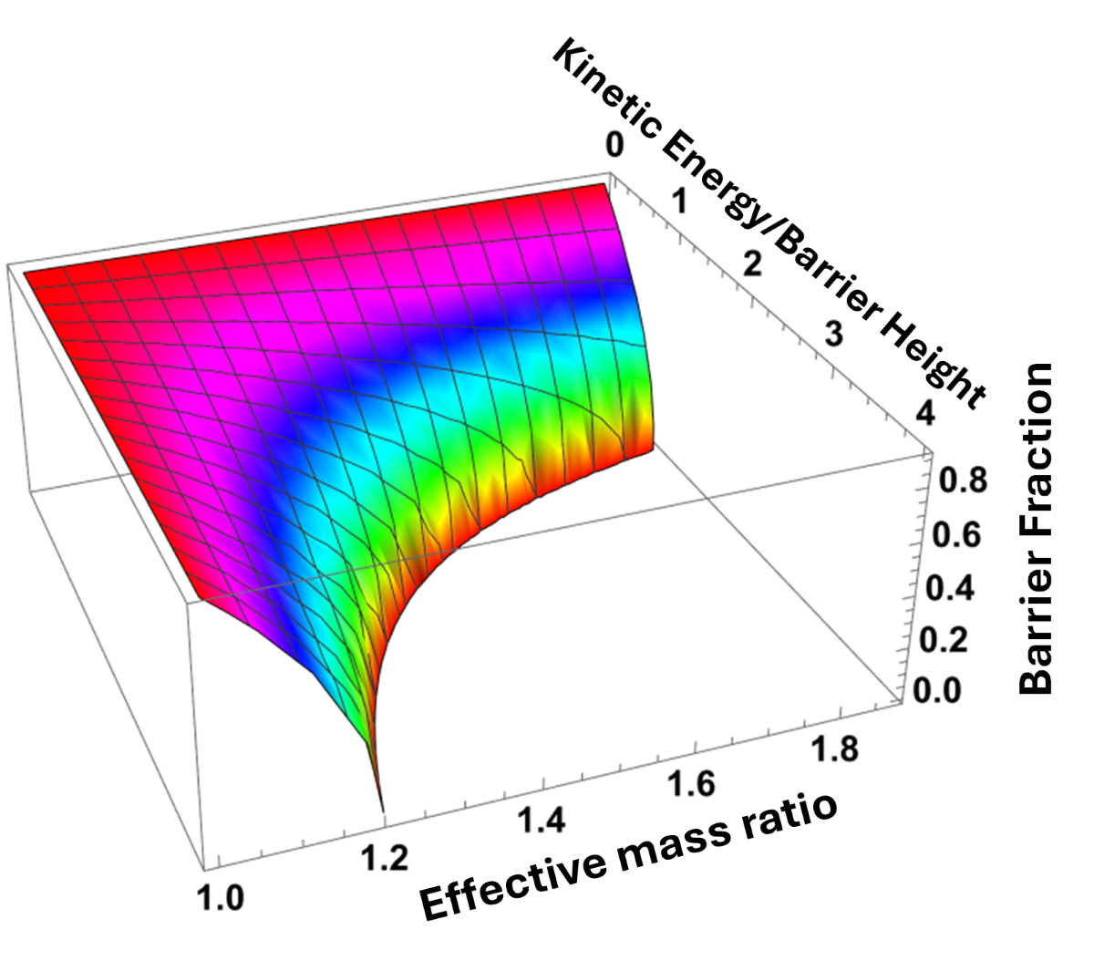
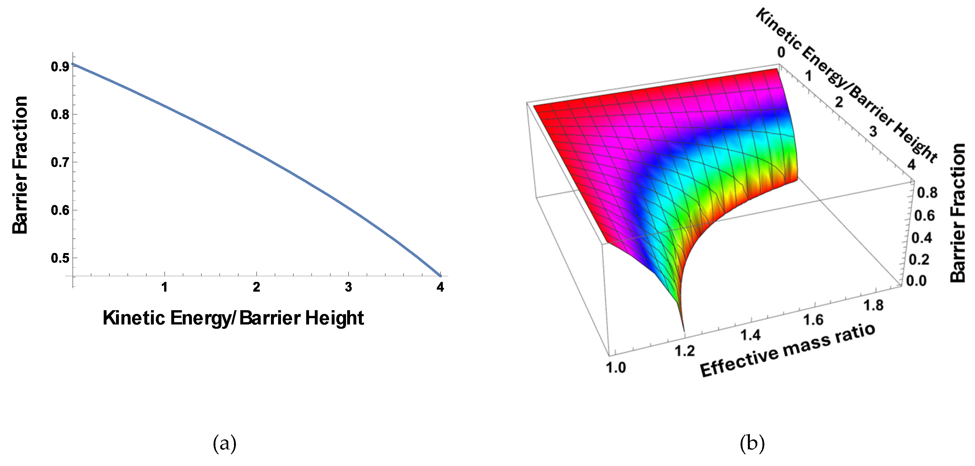
An additional important mechanism enhancing the breakdown field is the effect that we call the electron quantum real space transfer into the Al0.87Ga0.13 barrier layer. As shown in [29], a larger density of states in quantum well cladding layers causes an increase of the wave function penetration into the cladding layers with an increase in the electron kinetic energy EEEEE where k is the electron momentum in the channel plane. This transfer reduces the effective barrier height and completely eliminates the effective barrier for energetic electrons capable of causing impact ionization in the channel. The fraction of the remaining barrier height fb is a function of the channel electrons kinetic energy Ekin to the barrier height VB ratio: 29
Here mB and mEFF are the electron effective masses in the barrier and channel layers. In Figure 14(a) we plotted the effective barrier reduction for the device parameters of our QC HEMT. As seen, the effective barrier disappears for electrons with . Electrons causing impact ionization have kinetic energy Ekin > 6.2 eV or . Therefore, all very energetic electrons responsible for ionization should transfer into the cladding layer and the expected breakdown field should be equal to the breakdown field in the cladding layer, in agreement with the measured breakdown field.
Figure 14(b) shows the barrier reduction as a function of both e1 and . The upper bound of the range of 1,87 corresponds to the effective mass ratio of AlN and GaN. As seen from the figure, a large difference in Al molar fraction between the barrier and the channel is beneficial for the quantum real transfer. Such designs having an additional advantage of having much higher electron mobility in the device channel could be achieved by making the channel thinner to avoid the development of the dislocation arrays.
2. Conclusions
In conclusion, the QC Extreme Bandgap AlGaN HEMT design demonstrated the possibility to considerably improve the breakdown voltage. QC HEMT approach also has a strong potential to increase field-effect mobility, and, therefore, transconductance at low electron sheet densities and support a large maximum electron sheet density and a larger maximum current. A thinner quantum well made of lower bandgap material should also lead to better radiation hardness of QC HEMT.
Author Contributions
Conceptualization, M. Shur and G. Simin; methodology, G. Simin, A. Khan, MVS Chandrashekhar; validation, K. Hussain, A. Mamun. All authors have read and agreed to the published version of the manuscript.
Funding
This research at USC was funded by Office of Naval Research (ONR) Multidisciplinary University Research Initiatives (MURI) contract ONR N00014-18-1-2033, Program Manager Capt. L. Petersen, by Army Research Office contract W911NF-18-1-0029, Program Manager Dr. M. Gerhold. The work at RPI and USC was supported by the Office of Naval Research grant “STEM-Quantum Channel High Breakdown Voltage HEMT” N00014-23-1-2289-P00001 monitored by Dr. P. Maki.
Data Availability Statement
Data are contained within the article.
Conflicts of Interest
The authors declare no conflicts of interest.
References
- M. A. Khan, J. N. Kuznia, D. T. Olson, W. Schaff, J. Burm, M. S. Shur, Microwave Performance of 0.25-micron Doped Channel GaN/AlGaN Heterostructure Field Effect Transistor, Appl. Phys. Lett, Vol. 65 (9), pp. 1121-1123 (1994).
- M. S. Shur and M. Asif Khan, AlGaN/GaN Doped Channel Heterostructure Field Effect Transistors, Physica Scripta, T69, 103-107 (1997). [CrossRef]
- W. Saito, Y. Takada, M. Kuraguchi, K. Tsuda, I. Omura, T. Ogura, and H. Ohashi, “High breakdown voltage AlGaN–GaN power-HEMT design and high current density switching behavior,” IEEE Trans. Electron Devices, vol. 50, no. 12, pp. 2528–2531, Dec. 2003. [CrossRef]
- N. Tipirneni, V. Adivarahan, G. Simin and A. Khan, Silicon Dioxide Encapsulated High Voltage AlGaN/GaN HFETs for Power Switching Applications, IEEE El. Dev. Lett. V. 28, 784-786 (2007). [CrossRef]
- P.-C. Chao, Chu, K. Creamer, C. Diaz, J. Yurovchak, T. Shur, M. Kallaher, R. McGray, C. Via, G.D. Blevins, J.D. Low-Temperature Bonded GaN-on-Diamond HEMTs with 11 W/mm Output Power at 10 GHz, IEEE Transactions on Electron Devices, Volume: 62, Issue: 11, Pages: 3658-3664 (2015). [CrossRef]
- Mishra U, Shen L, Kazior T, Wu Y. GaN-based RF power devices and amplifiers. Proc IEEE 2008;96:287–305.
- Y.-F. Wu, B.P. Keller, P. Fini, J. Pusl, M. Le, N. X. Nguyen, C. Nguyen, D. Widman, S. Keller, S. P. Denbaars, and U. K. Mishra, Short-channel Al0.5Ga0.5N/GaN MODFETs with power density > 3 W/mm at 18 GHz Electron. Lett. 33 p. 1742 (1997).
- Mishra U, Shen L, Kazior T, Wu Y. GaN-based RF power devices and amplifiers. Proc IEEE 2008;96:287–305.
- S. J. Pearton et al, Review—Ionizing Radiation Damage Effects on GaN Devices 2016 ECS J. Solid State Sci. Technol. 5 Q35 DOI 10.1149/2.0251602jss. [CrossRef]
- Sequeira, M. C., Mattei, J., Vazquez, H., Djurabekova, F., Nordlund, K., Monnet, I., Kluth, P., Grygiel, C., Zhang, S., Alves, E., & Lorenz, K. (2021). Unravelling the secrets of the resistance of GaN to strongly ionising radiation. Communications Physics, 4(1), 1-8. [CrossRef]
- A. Bykhovski, B. Gelmont, and M. S. Shur, The Influence of the Strain-Induced Electric Field on the Charge Distribution in GaN-AlN-GaN SIS Structure, J. Appl. Phys. Dec. Vol. 74 (11), p. 6734-6739 (1993).
- O. Ambacher; B. Foutz; J. Smart; J. R. Shealy; N. G. Weimann; K. Chu; M. Murphy; A. J. Sierakowski; W. J. Schaff; L. F. Eastman; R. Dimitrov; A. Mitchell; M. Stutzmann, Two-dimensional electron gases induced by spontaneous and piezoelectric polarization in undoped and doped AlGaN/GaN heterostructures. J. Appl. Phys. 87, 334–344 (2000), . [CrossRef]
- M. E. Levinshtein, S. L. Rumyantsev, and M. S. Shur, Editors, “Properties of Advanced Semiconductor Materials: GaN, AlN, InN, BN, SiC, and SiGe“, J. Wiley and Sons, ISBN 0-471-35827-4, New York (2001).
- M. E. Levinshtein, S. Rumyantsev, and M. S. Shur, Editors, Handbook of Semiconductor Material Parameters, Si, Ge, C (diamond), GaAs, GaP, GaSb, InAs, InP, InSb, Vol. 1, World Scientific, 1996, ISBN981-02-2934-8517.
- P.A. Ivanov, M.E. Levinshtein, G. Simin, X. Hu, J. Yang, M. A. Khan, S. L. Rumyantsev, M. S. Shur and R. Gaska, Drift mobility of electrons in AlGaN/GaN MOSHFET, Electronics Letters, vol. 37 (24), pp. 1479-1481 (2001). [CrossRef]
- E. Frayssinet, W. Knap, P. Lorenzini, N. Grandjean and J. Massies, C. Skierbiszewski, T. Suski, I. Grzegory, S. Porowski, G. Simin, X. Hu, M. A. Khan, M. Shur, R. Gaska, and D. Maude, High electron mobility in AlGaN/GaN heterostructures grown on bulk GaN substrates, Appl. Phys. Lett, Vol. 77, No. 16, pp. 2551-2553, October (2000). [CrossRef]
- R. Gaska, M. S. Shur, A. D. Bykhovski, A. O. Orlov, and G. L. Snider, Electron Mobility in Modulation Doped AlGaN-GaN Heterostructures, Appl. Phys. Lett. 74, No. 2, January 11, pp. 287-289 (1999).
- A. Azimi, M. Azimi, M. S. Shur, and S. K. O’Leary. The impact of device length on the electron's effective mobility, J. App. Phys., 134, 125701 (2023), . [CrossRef]
- Hussain, Kamal, et al. "High figure of merit extreme bandgap Al0. 87Ga0. 13N-Al0. 64Ga0. 36N heterostructures over bulk AlN substrates." Applied Physics Express 16.1 (2023): 014005.
- Mamun, Abdullah, et al. "Al0. 64 Ga0. 36N channel MOSHFET on single crystal bulk AlN substrate." Applied Physics Express 16.6 (2023): 061001.
- R. Gaska, C. Chen, J. Yang, E. Kuokstis, A. Khan, G. Tamulaitis, I. Yilmaz, M. S. Shur, J. C. Rojo, L. Schowalter, Deep-ultraviolet emission of AlGaN/AlN quantum wells on bulk AlN, Appl. Phys. Lett. Vol. 81, No 24, pp. 4658-4660, (2002). [CrossRef]
- X. Hu, J. Deng, N. Pala, R. Gaska, M. S. Shur, C. Q. Chen, J. Yang, S. Simin, and A. Khan, C. Rojo, L. Schowalter, AlGaN/GaN Heterostructure Field Effect Transistor on Single Crystal Bulk AlN, Appl. Phys. Lett, 82, No 8, pp. 1299-1302, 24 Feb (2003). [CrossRef]
- G. Tamulaitis, I. Yilmaz, M. S. Shur, R. Gaska, C. Chen, J. Yang, E. Kuokstis, A. Khan, S.B. Schujman, L. J. Schowalter, Photoluminescence of GaN Deposited on Single Crystal Bulk AlN with Different Polarities, Appl. Phys. Lett. 83, No 17, pp. 3507-3509 (2003). [CrossRef]
- M. S. Shur, Introduction to Electronic Devices, J. Wiley and Sons, New York, 1996, ISBN 0-471-10348-9, ISBN 981-02-2325.
- K. Lee, M. S. Shur, T. A. Fjeldly, and T. Ytterdal, Semiconductor Device Modeling for VLSI, Prentice Hall, Englewood Cliffs, NJ (1993).
- G. Snider, 1D Poisson - a program for calculating energy band diagrams for semiconductor structures. https://www3.nd.edu/~gsnider/, accessed October 10, 2023.
- J. L. Hudgins, G.S. Simin, E. Santi, M. Asif Khan, An Assessment of Wide bandgap Semiconductors for Power Devices, IEEE Trans. on Power Electronics, V.18, 907-914 (2003). [CrossRef]
- W. A. Hadi, M. S. Shur, and S. K. O’Leary Review: Steady-state and transient electron transport within the wide energy gap compound semiconductors gallium nitride and zinc oxide: An updated and critical review, Journal of Materials Science: Materials in Electronics, J Mater Sci: Mater Electron (2014) 25:4675–4713 . [CrossRef]
- M. Dyakonov and M. S. Shur, Consequences of space dependence of effective mass in heterostructures, J. Appl. Phys, V 84, N7, p. 3726 (1998). [CrossRef]
- P.A. Ivanov, M.E. Levinshtein, G. Simin, X. Hu, J. Yang, M. A. Khan, S. L. Rumyantsev, M. S. Shur and R. Gaska, Drift mobility of electrons in AlGaN/GaN MOSHFET, Electronics Letters, vol. 37 (24), pp. 1479-1481 (2001). [CrossRef]
- C. Chen, J. Zhang, V. Adivarahan, A. Koudymov, H. Fatima, G. Simin, J. Yang, and M. Asif Khan, AlGaN/GaN/AlGaN Double Heterostructure for high power III-N FETs, Appl. Phys. Lett. 82, 4593 (2003).
- F. Yun et. al. Energy band bowing parameter in AlxGa1− xN alloys Appl. Phys. 92, 4837 (2002).
- J. Davies, The Physics of Low-Dimensional Semiconductors, Cambridge University Press (1998).
Figure 1.
Conventional (a) and QC-HEMT (b) designs. QC-HEMT in Figure 1(b) can have GaN or AlGaN channel (GaN channel is shown).
Figure 1.
Conventional (a) and QC-HEMT (b) designs. QC-HEMT in Figure 1(b) can have GaN or AlGaN channel (GaN channel is shown).
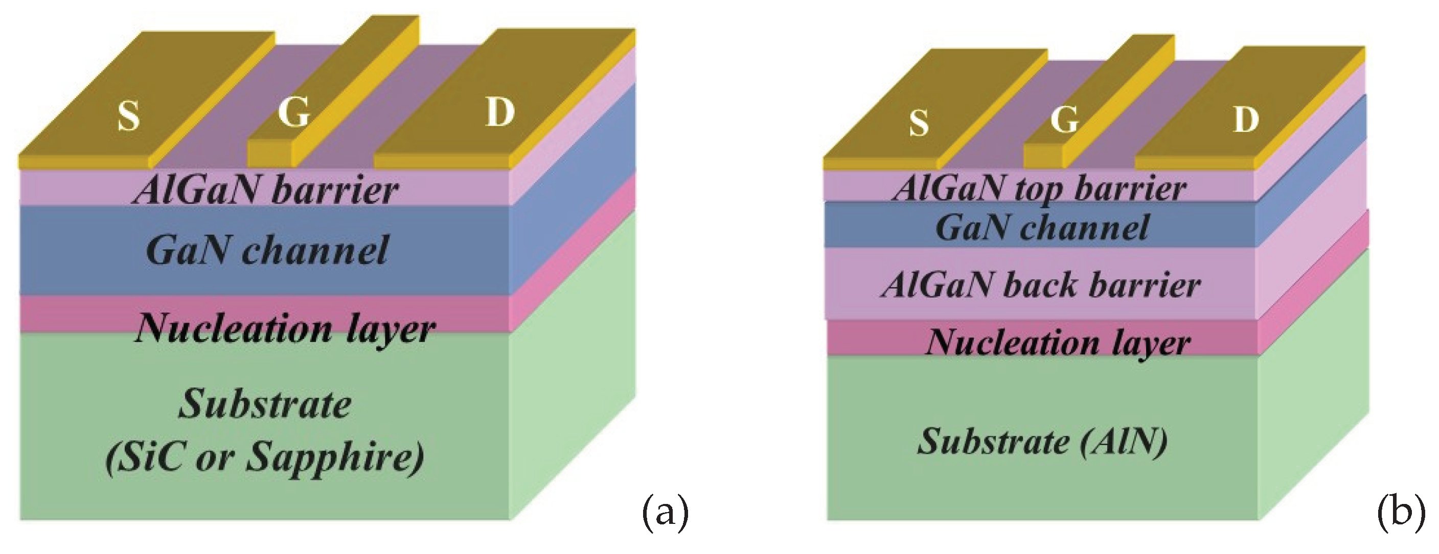
Figure 2.
Energy band diagrams of QC-HEMT with channel thickness 2 nm. The dashed lines show ground state energy E0 at different gate voltages.
Figure 2.
Energy band diagrams of QC-HEMT with channel thickness 2 nm. The dashed lines show ground state energy E0 at different gate voltages.
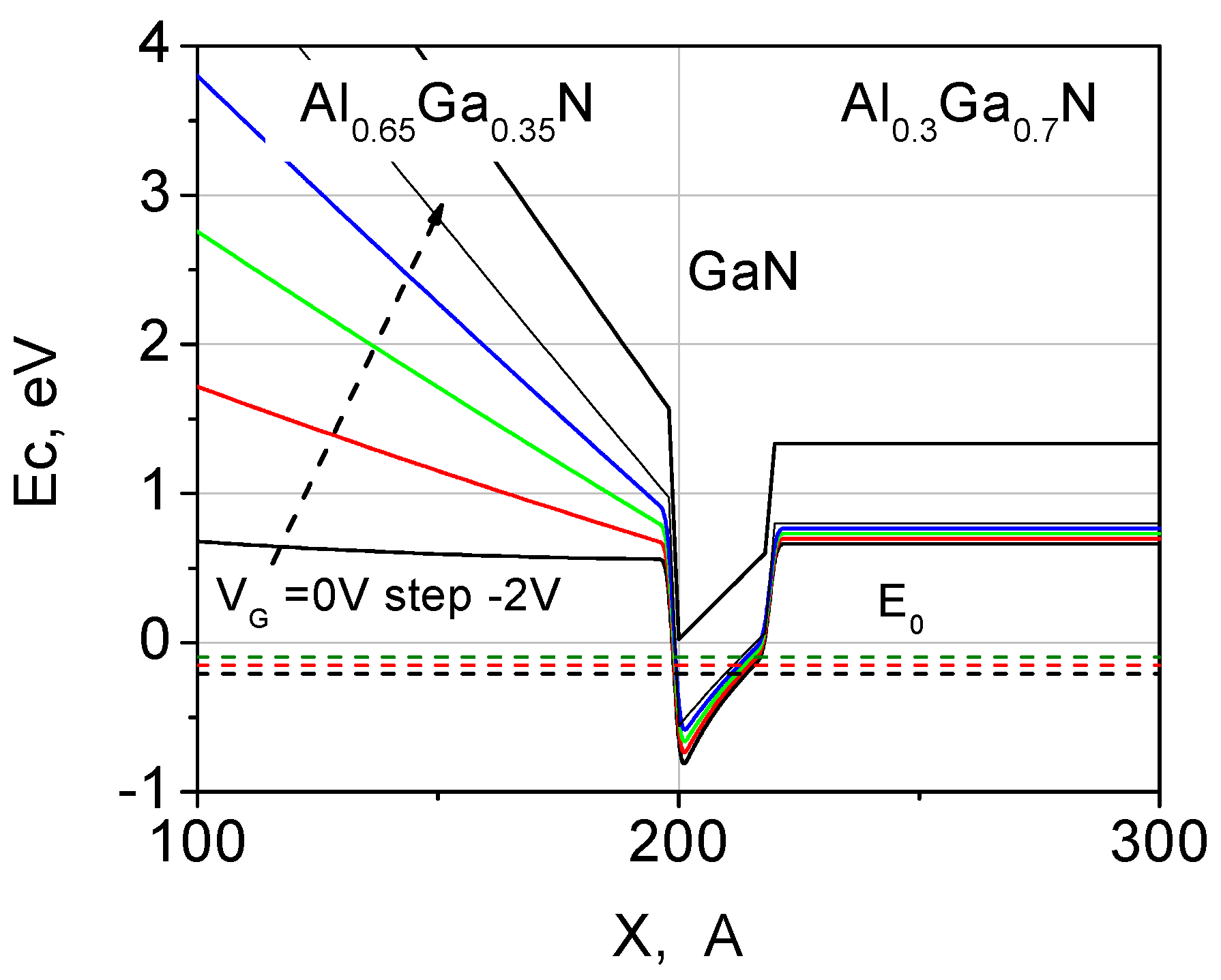
Figure 3.
Dependencies of the ground state energy E0 above the bottom of the conduction band on the sheet carrier concentration nS for the conventional HEMT and the QC HEMT with a 2 nm thick channel.
Figure 3.
Dependencies of the ground state energy E0 above the bottom of the conduction band on the sheet carrier concentration nS for the conventional HEMT and the QC HEMT with a 2 nm thick channel.
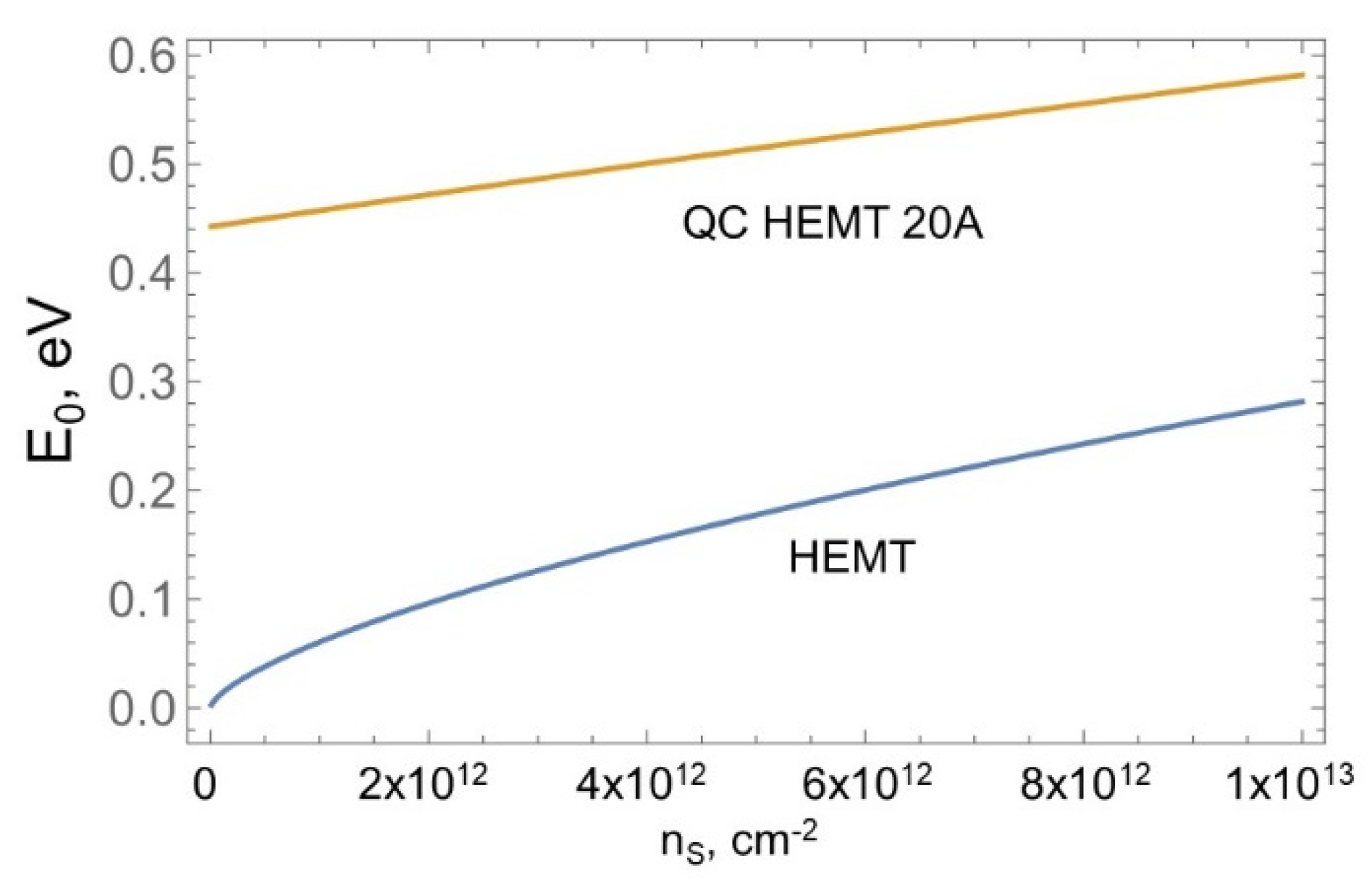
Figure 4.
Electron wave function for the QC HEMT with 2 nm thick channel. Several curves (nearly overlapping) correspond to different gate voltages VG. As seen, the wave function profile is practically independent of VG.
Figure 4.
Electron wave function for the QC HEMT with 2 nm thick channel. Several curves (nearly overlapping) correspond to different gate voltages VG. As seen, the wave function profile is practically independent of VG.
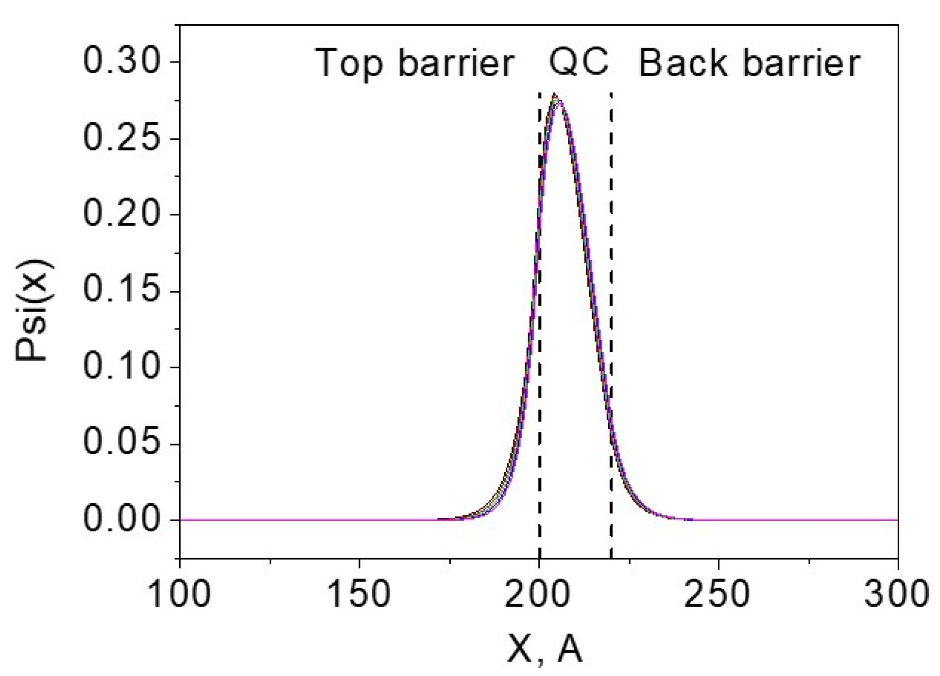
Figure 5.
2DEG volume electron density as a function of ns in conventional and QC HEMTs.
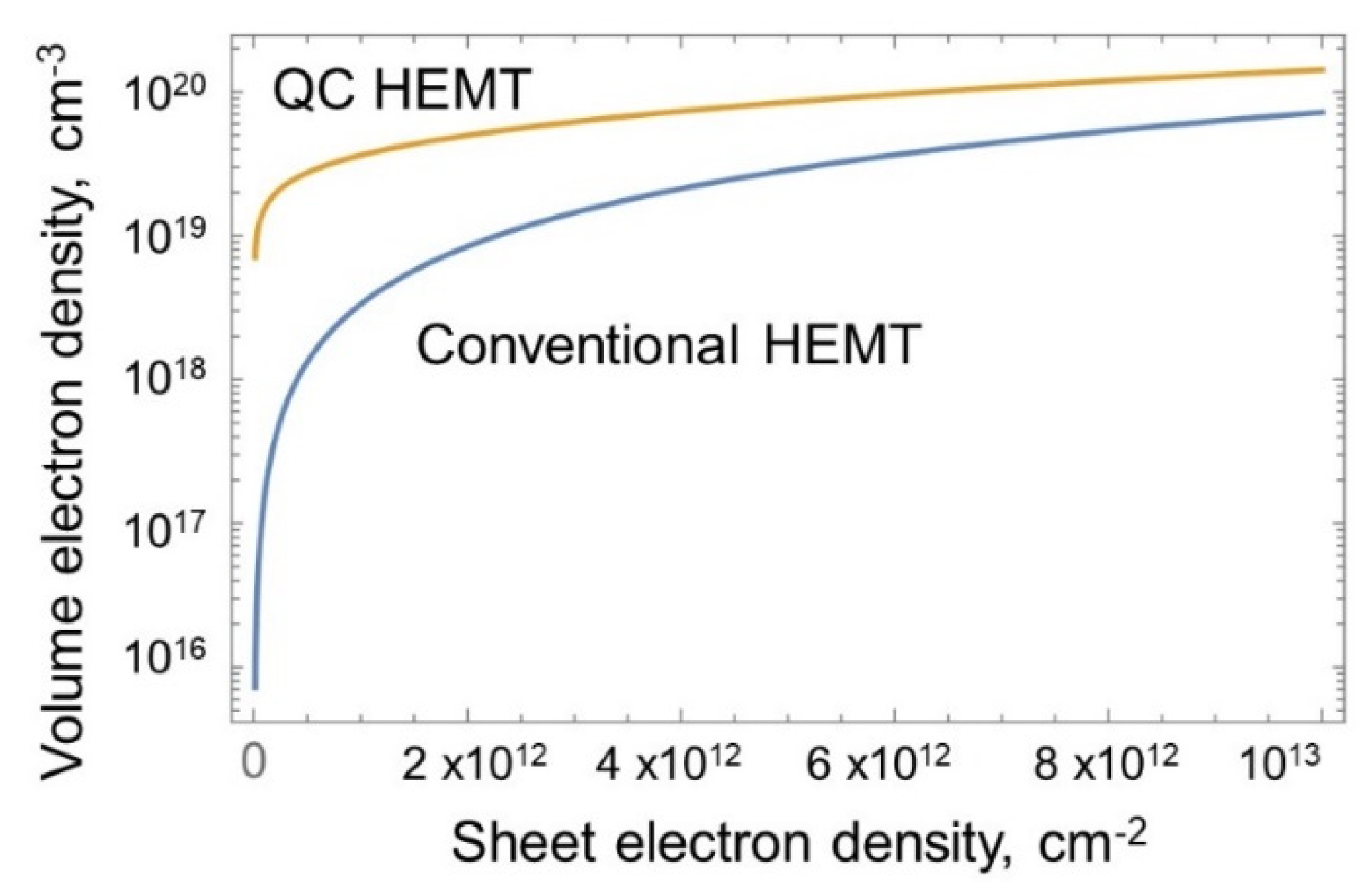
Figure 6.
(a) Expected mobility increase in QC HEMT; (b) experimentally observed mobility increase in double-heterostructure (DH) HEMT.
Figure 6.
(a) Expected mobility increase in QC HEMT; (b) experimentally observed mobility increase in double-heterostructure (DH) HEMT.
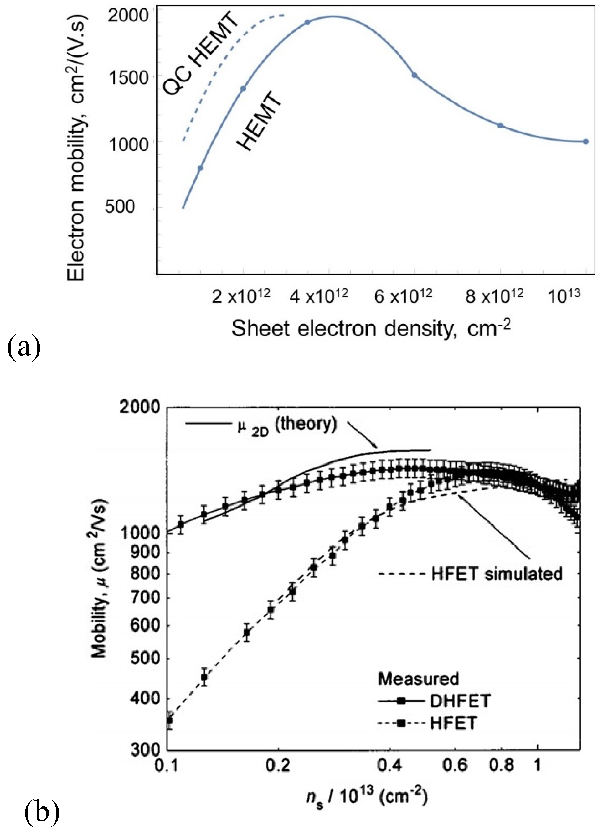
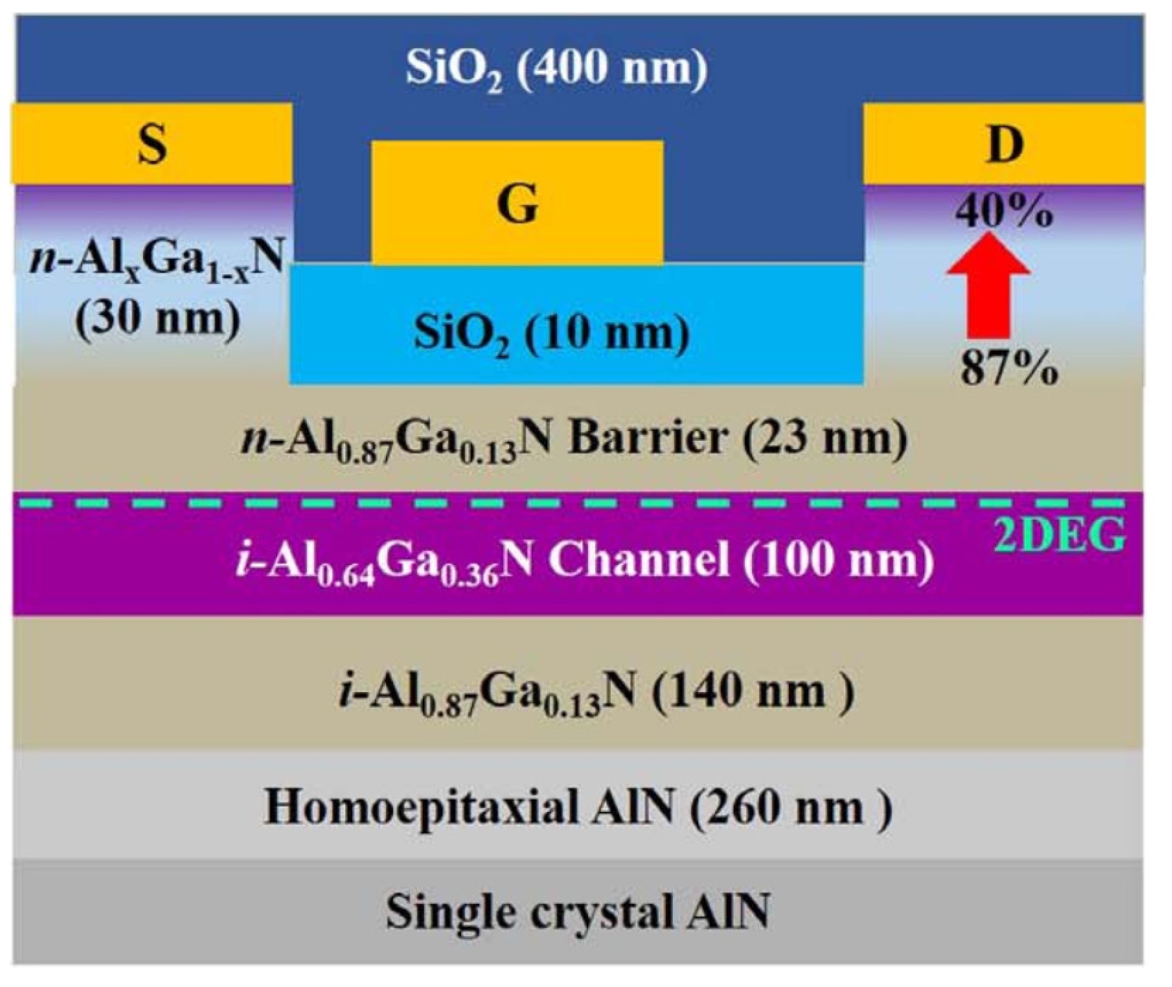
Figure 8.
EBG HEMT breakdown current-voltage characteristics [1].
Figure 8.
EBG HEMT breakdown current-voltage characteristics [1].
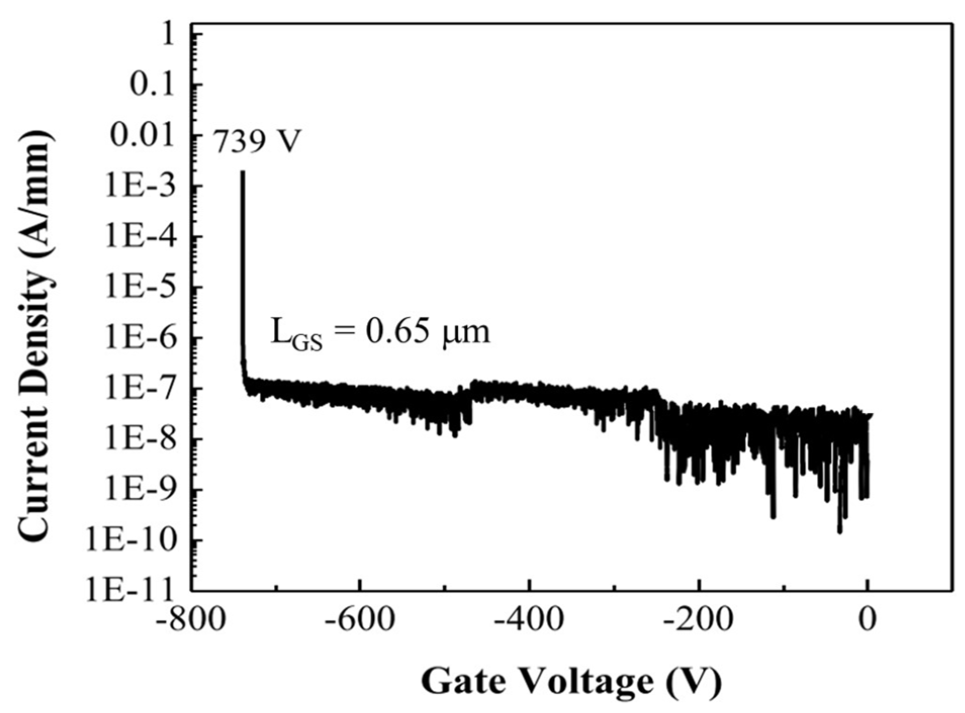
Figure 9.
EBG HEMT drain current ID (VD) (a), transfer ID (VG), and transconductance gm (VG) (b) characteristics [20].
Figure 9.
EBG HEMT drain current ID (VD) (a), transfer ID (VG), and transconductance gm (VG) (b) characteristics [20].
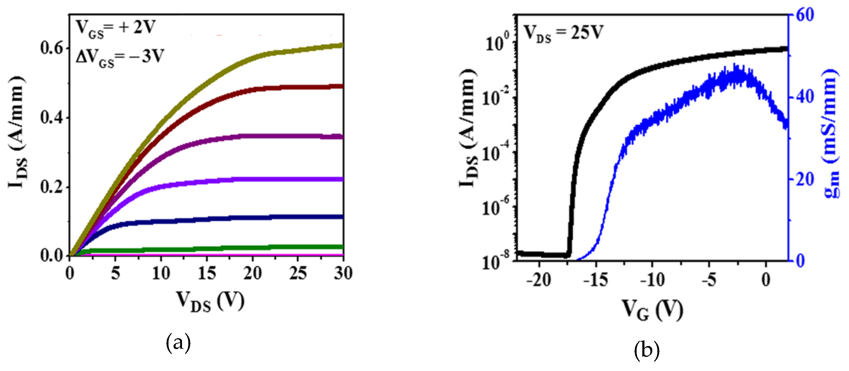
Figure 10.
2D HEMT model used in Synopsys simulations.
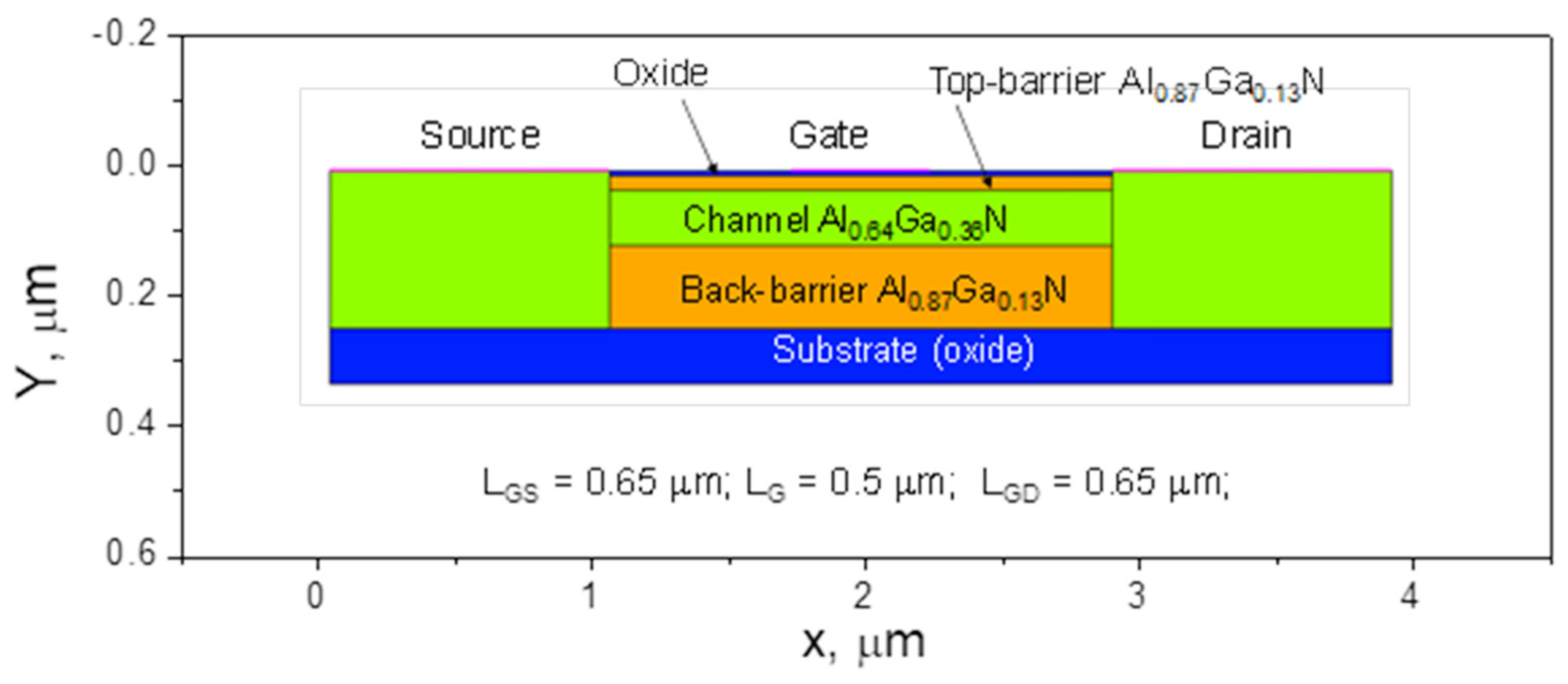
Figure 11.
Band diagram of the Quantum Channel HEMT under study at zero gate bias (a) and gate bias below threshold voltage (b). The top barrier/channel interface is at y=0.035 m (obtained using 2D simulations).
Figure 11.
Band diagram of the Quantum Channel HEMT under study at zero gate bias (a) and gate bias below threshold voltage (b). The top barrier/channel interface is at y=0.035 m (obtained using 2D simulations).
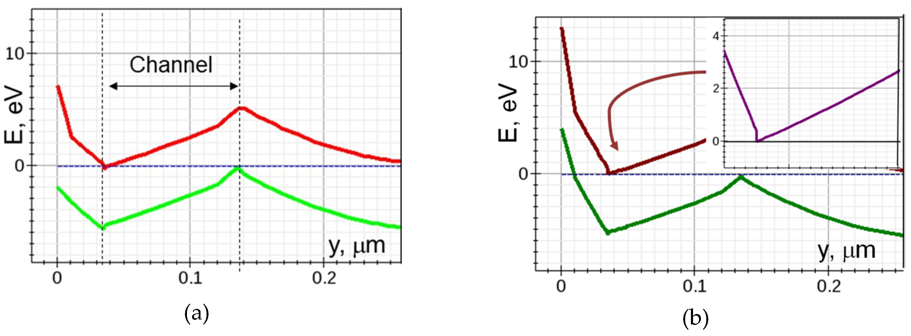
Figure 12.
Band diagram of conventional Al0.25Ga0.75N/GaN HEMT at zero gate bias (a) and gate bias below the threshold voltage (b). The barrier/channel interface is at y=0.073 m (obtained using 2D simulations).
Figure 12.
Band diagram of conventional Al0.25Ga0.75N/GaN HEMT at zero gate bias (a) and gate bias below the threshold voltage (b). The barrier/channel interface is at y=0.073 m (obtained using 2D simulations).
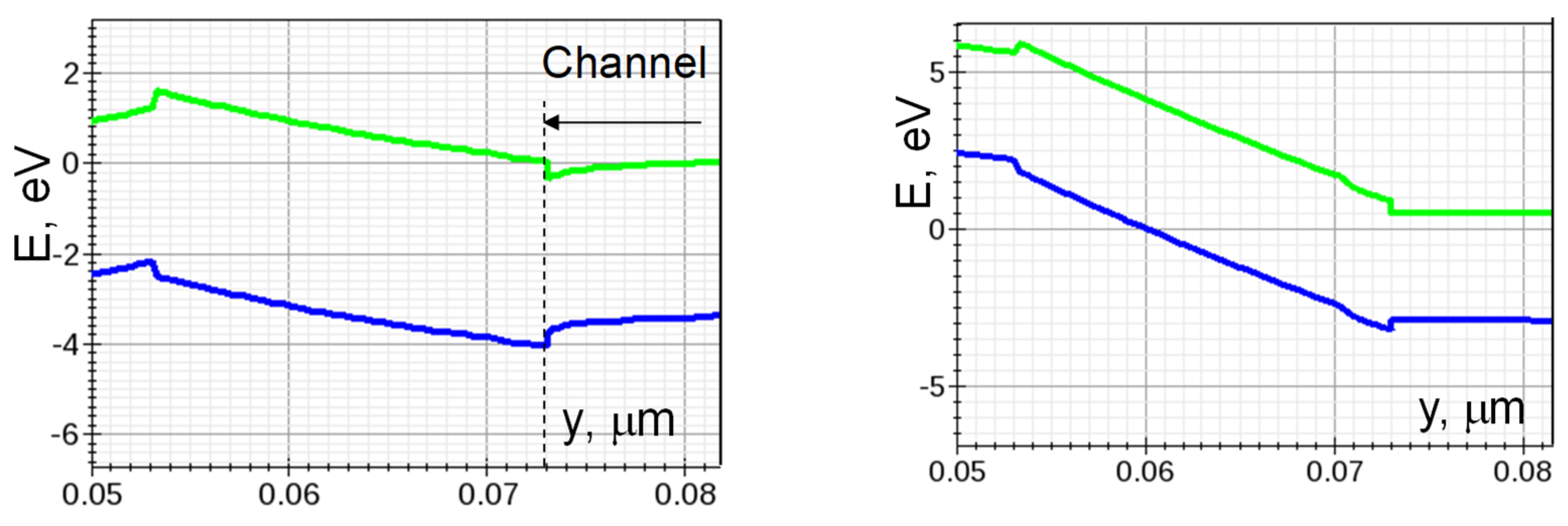
Figure 13.
Triangular QW profile used in MATLAB calculations of the ground state energy E1. The barrier height at the Al0.87Ga0.13N/ Al0.64Ga0.36N barrier/channel interface, VB = 0.72 eV, electric field in the channel FCH = 0.5 MV/cm, electron effective mass in the channel, mEF = 0.34 m0.
Figure 13.
Triangular QW profile used in MATLAB calculations of the ground state energy E1. The barrier height at the Al0.87Ga0.13N/ Al0.64Ga0.36N barrier/channel interface, VB = 0.72 eV, electric field in the channel FCH = 0.5 MV/cm, electron effective mass in the channel, mEF = 0.34 m0.
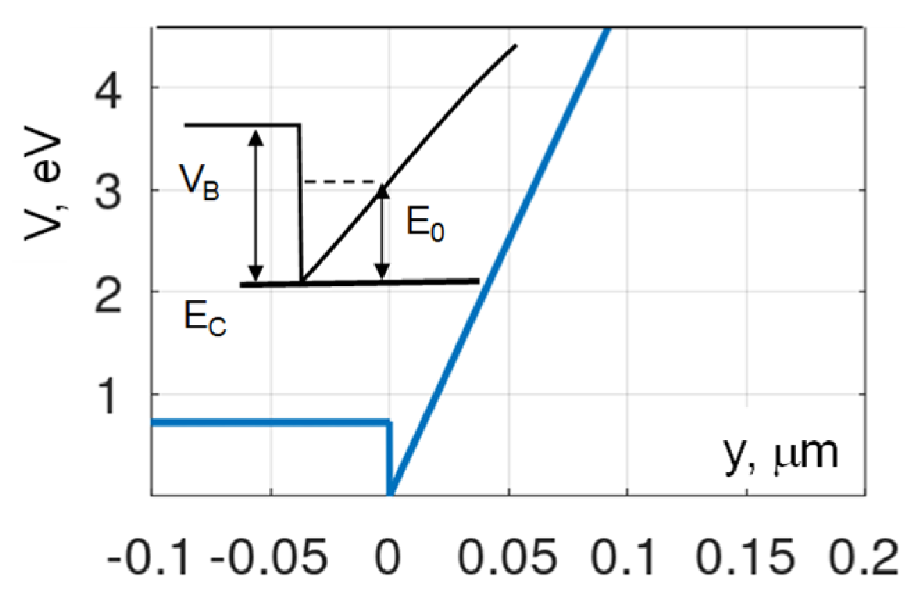
Figure 14.
Barrier reduction for energetic electrons: (a) versus kinetic energy of electrons in QC HEMT under study and (b)same for all mass ratios for AlN/GaN system.
Figure 14.
Barrier reduction for energetic electrons: (a) versus kinetic energy of electrons in QC HEMT under study and (b)same for all mass ratios for AlN/GaN system.
Disclaimer/Publisher’s Note: The statements, opinions and data contained in all publications are solely those of the individual author(s) and contributor(s) and not of MDPI and/or the editor(s). MDPI and/or the editor(s) disclaim responsibility for any injury to people or property resulting from any ideas, methods, instructions or products referred to in the content. |
© 2024 by the authors. Licensee MDPI, Basel, Switzerland. This article is an open access article distributed under the terms and conditions of the Creative Commons Attribution (CC BY) license (http://creativecommons.org/licenses/by/4.0/).
Copyright: This open access article is published under a Creative Commons CC BY 4.0 license, which permit the free download, distribution, and reuse, provided that the author and preprint are cited in any reuse.


