1. Introduction
Light detection and ranging (LiDAR) sensors have been exploited in various applications, such as unmanned autonomous vehicles, navigation systems for robots, indoor mapping on mobile devices, remote sensing, and home monitoring LiDAR sensors either for senile dementia patients residing in long-term care facilities [
1,
2,
3,
4]. In particular, the home monitoring sensors for senile dementia patients mandate to be very small and provide depth information in emergency, thus alarming the situations promptly to supervisors. For these purposes, a small, low-power, low-cost light detection and ranging (LiDAR) sensor can be a potential solution not only because its final images are blurred, thus avoiding image violation, but also because it can precisely provide every necessary information of single elders including move, fall, breath rate, and etc. In addition, it can provide a number of advantages over conventional RF sensors due to their robustness against large ambient RF interferences.
Most of LiDAR sensors utilize the principle of pulsed time-of-flight (ToF) mechanism, so that light pulses can be emitted from a transmitter to targets which are located within a feasible range whereas its reflected signals can be detected by an optical receiver. With the speed of light known, the target distance can be measured by the time-interval between the transmitted (or START) pulse and its reflected (or STOP) pulse. The typical detection range of an indoor LiDAR sensor at home is 0.2~5 meters. Therefore, the dynamic range of the received pulses (or echoes) should be wide enough (i.e., 1:625 [
5]), thus mandating fast response.
Previously, a number of analog front-end optical receivers have been suggested [
6,
7,
8,
9,
10,
11,
12,
13,
14,
15], in which off-chip avalanche photodiodes (APDs) were mostly integrated on PC-boards via bond-wires. However, this bond-wire interconnection may lead to considerable increase of packaging cost in the cases of multi-channel receiver arrays, and mandate on-chip electrostatic discharge protection diodes which, however, deteriorate the receiver bandwidth and worsen the noise performance. Also, various time-to-digital converters (TDCs) were presented to precisely estimate the time-interval between the START and the STOP pulses, hence enabling accurate range detection [
16,
17,
18]. However, they mostly mandated complicated algorithms and hence the complex circuit designs to satisfy the specification requirements since they particularly aimed to accomplish the significant reduction of notorious walk-errors that typically occurred at the comparators in TDCs. Nonetheless, the finite rising (or falling) edges of the STOP pulses could not prevent the walk-error issues completely even from the novel TDCs. In this paper, we propose a simpler and less complicated design methodology for a multi-channel optical readout array (ORA) in the applications of short-range LiDAR sensors.
This paper is organized as follows. Section II describes the circuit operations of the proposed optoelectronic readout array along with the on-chip P+/N-well APD. Section III presents the chip layout and the post-layout simulation results of the ORA. Section IV demonstrates the measured results of the fabricated chips. Then, a conclusion is followed in Section V.
2. Circuit Description
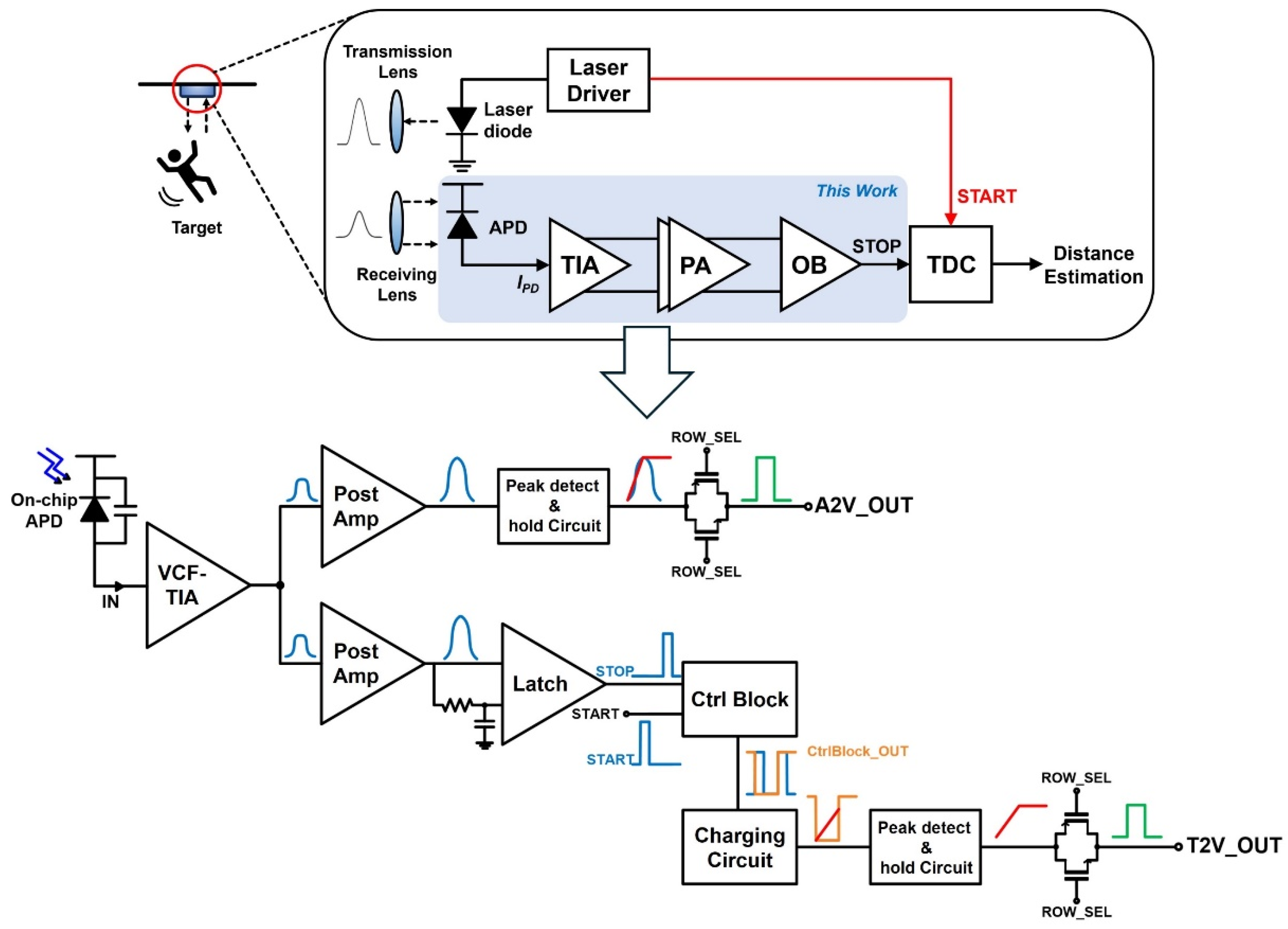
Figure 1a shows the block diagram of a typical LiDAR sensor system, in which the laser diode driver emits light pulses to a target that is a senior in this figure. Thereafter, the reflected light pulses are detected by an on-chip optical detector, i.e., APD in the receiver. The corresponding photocurrents generated from the APD are converted to voltage signals and amplified by an analog frontend circuit that comprises a transimpedance amplifier (TIA) and a post-amplifier (PA). Finally, a TDC estimates the distance to targets by measuring the time-interval between the emitted pulse and the reflected one.
In this work, an 8x8 channel optoelectronic readout array (ORA) is presented for indoor-monitoring LiDAR sensor applications, of which single cell comprises an on-chip P
+/N-well APD, a voltage-mode CMOS feedforward transimpedance amplifier (VCF-TIA), an amplitude-to-voltage (A2V) converter, and a time-to-voltage (T2V) converter.
Figure 1b depicts the block diagram of the single cell in the proposed 8x8 CMOS ORA, where the A2V converter consists of a post-amplifier (PA), a peak-detect and hold (PDH) circuit, and a transmission gate (TG) for selection while the T2V converter comprises a PA, a latch, a control block, a charging circuit, a PDH, and a TG, respectively.
In particular, the A2V is suggested to convert linearly the small input photocurrents (from 5 to 500 μApp) to output voltages and thereafter hold the peak values until the reset signal enters. Thereby, the A2V is effective to detect weak signals reflected from the target located within 8.2 meters. Yet, it cannot recover the signals larger than 500 μApp that corresponds to 82 centi-meters. In order to extend the dynamic range for large input currents, the T2V converter is newly proposed to decode the time intervals between the START and STOP signals to output voltages and then hold the peak values. This T2V can recover the relatively large input currents from 50 μApp to 1.1 mApp that corresponds to the minimum detection range of 56 centi-meters. Namely, the proposed ORA can successfully recover optical pulses reflected from the targets located within the detection range of 0.56 ~ 8.2 meters.
A. On-Chip APD
Figure 2 depicts the cross-sectional view of the on-chip P
+/N-well (NW) CMOS APDs and its layout, in which the P
+/N-well junction structure is exploited due to its several advantages such as a shallow trench isolation (STI) as a guard ring to enhance avalanche gain and a narrow depletion region in the NW to increase bandwidth [
13]. The P
+ node is connected to the TIA input to convey the current pulses, whereas the P-substrate is connected to AC-ground to prevent slow diffusion currents. A high voltage is applied to the NW to obtain the reverse bias of the P
+/NW junction. As depicted in
Figure 2b, an octagonal shape of the on-chip P
+/NW APD is preferred to avoid the edge-breakdown phenomenon. Its optical window (with 40-μm diagonal line) is created by using a salicide blocking layer. Also, the silicide layer is applied to the P
+ node to reduce the parasitic resistance. As reported in prior arts [
13,
19], the fabricated on-chip P
+/NW APD in a standard 180-nm CMOS process exhibits the parasitic capacitance of 0.49 pF and the responsivity of 2.72 A/W at a bias voltage of 11.05 V with the avalanche breakdown voltage of 11.1 V.
B. VCF-TIA
Figure 3a illustrates the schematic diagram of the VCF-TIA followed by an inverter-based post-amplifier (PA). The VCF-TIA employs a conventional voltage-mode inverter (INV) input stage which includes a feedback resistor (R
F) and a feedforward common-source (CS) amplifier, as described in [
5]. The gate of this CS amplifier is connected to the gates of the INV stage, where R
G represents the series resistance is incorporated not only because the gate resistance provides damping to the input inductance, thereby preventing oscillation, but also because it aids in defining the bandwidth to meet the desired specification for the recovery of narrow laser pulses (i.e., 5 ns). In addition, R
L is selected to be in the range of several tens of kilo-ohm, ensuring that the large DC current (I
M2) flows through M
2. This would help to enhance the transconductance (g
m2) because the DC drain voltage of M2 is fixed by the mechanism of the INV amplifier with a feedback resistor. Consequently, the increased transconductance (g
m2) of M
2 lowers the input resistance of the VCF-TIA and minimizes the noise contribution from M
2.
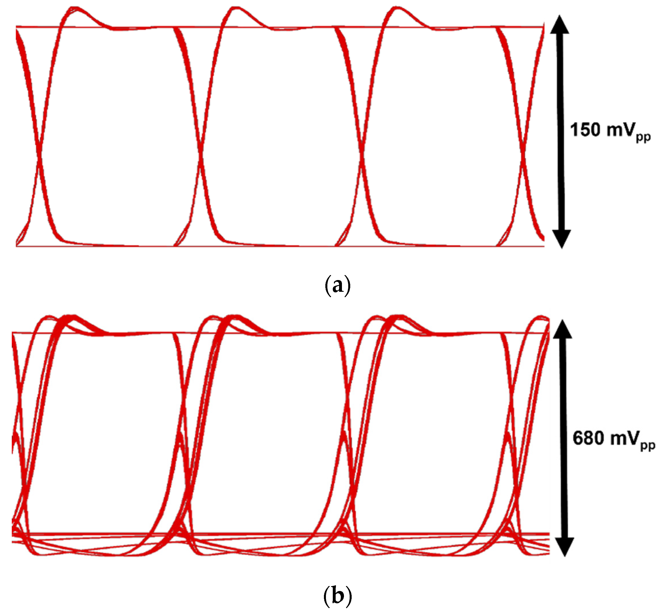
Figure 4 illustrates the simulated eye-diagrams of the VCF-TIA at 200 Mb/s data rate for two different input currents of 100 μA
pp and 1 mA
pp, respectively. These results confirm that the VCF-TIA can recover the eyes even for the large input currents.
C. A2V (Amplitude-to-Voltage) Converter
As aforementione, the proposed A2V converter consists of a VCF-TIA, a post-amplifier (PA), and a peak detect and hold (PDH) circuit.
Figure 3b depicts the schematic diagram of the PDH circuit which basically shares the topology of a two-stage operational amplifier except that the load is a series combination of a resistor (R
3) and a capacitor (C) for peak detection. Subsequently, the PDH circuit generates the final output pulses that correspond to the amplitudes of the incoming photocurrents. The primary objective of this A2V converter is to facilitate the detection of targets located at a rather longer distance in LiDAR sensor applications.
For this purpose, the PA gain is approximately 10 dB, thus providing a threefold increase in the signal amplitude. It should be noted that the balance of the gain settings in each block is very crucial to maintain signal linearity and hence to ensure accurate distance estimation based on signal amplitudes.
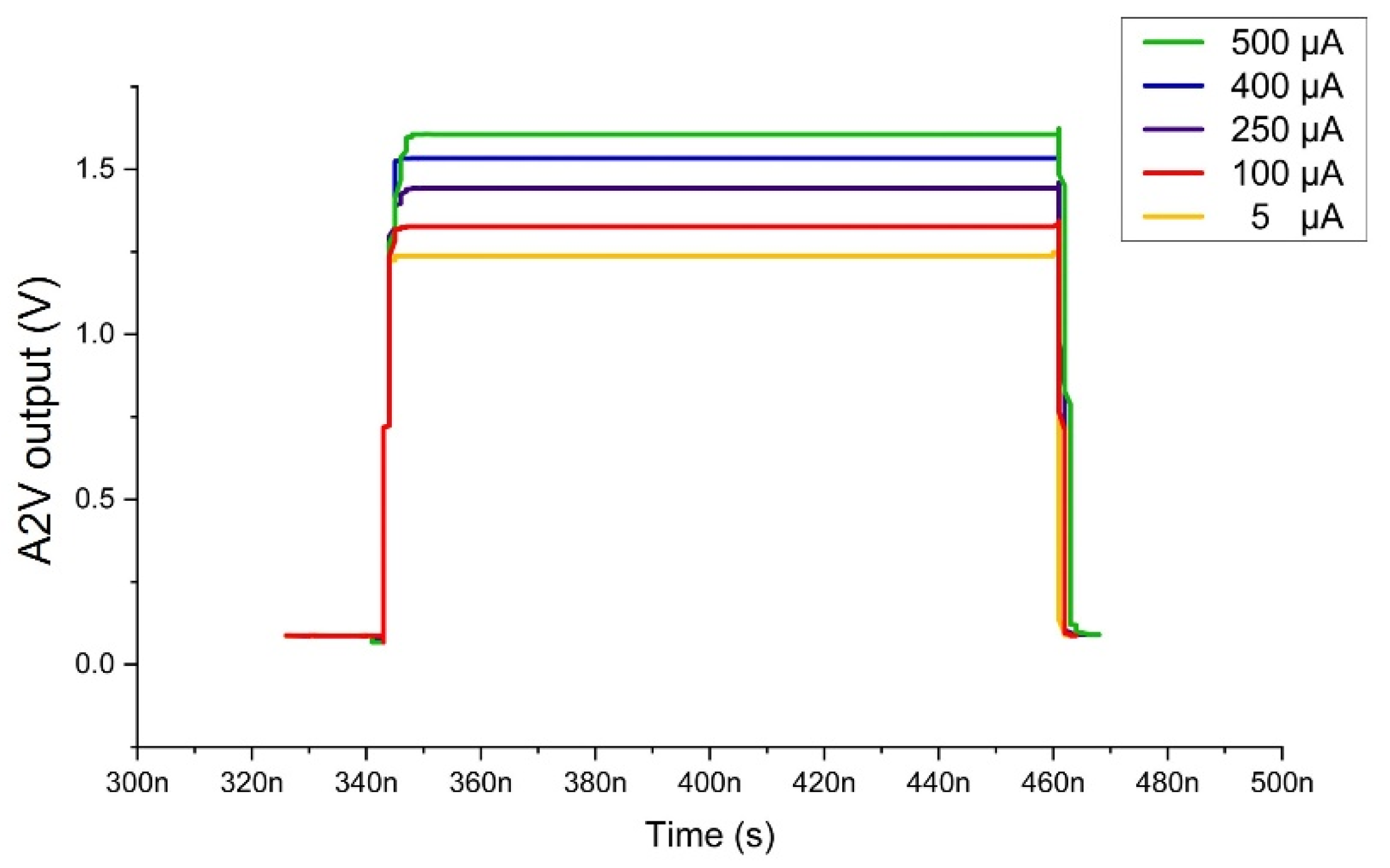
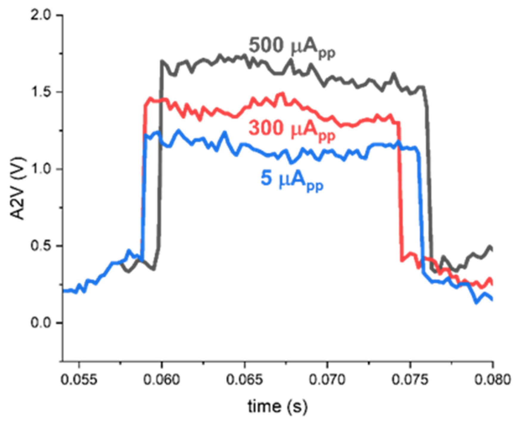
Figure 5 shows the post-layout simulation results which validate the anticipated capability of the A2V converter for the input photocurrents from 5 μA
pp to 500 μA
pp with an almost linear step with the aid of gain control scheme, maintaining the signal integrity and providing the precise distance measurements. These input currents correspond to the detection ranges from 0.82 to 8.2 meters.
D. T2V (Time-to-Voltage) Converter
The proposed T2V converter is a crucial component to extend the input dynamic range of the proposed ORA, because it is responsible for converting the time-of-flight information into the corresponding output pulses. Namely, the initial photocurrents generated by the on-chip APD are converted to voltage signals by the VCF-TIA. Then, these voltage signals enter the PA for further gain-boosting. Unlike the A2V path, the proposed T2V converter requires only the detection of signal presence. Therefore, the PA in the T2V path would have to ensure that the output signals would be reliably processed by the subsequent stages, irrespective of reaching the saturation. The output signals from the PA go into the latch that results in digital pulses. In other words, the latch yields ‘1’ when a signal is present whereas ‘0’ with no signals. Thereafter, the latch output is fed into the control block along with a START signal from the Tx. The control block is designed to provide ‘0’ outputs for the duration between the START pulse and the received STOP pulse. More specifically, the outputs of the control block switch to ‘0’, i.e., GND as soon as it receives the START pulse, and then remain at GND until the latch output pulse is detected. After the latch output detection, the control block switches output back to VDD. For simulations, arbitrary signals were utilized to simulate the Tx START pulses.
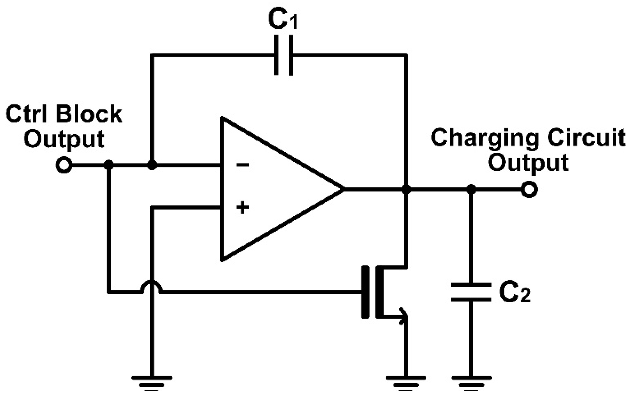
Figure 6 illustrates the schematic diagram of the charging circuit in the proposed T2V converter, which employs an operational amplifier with a capacitor-feedback. When the output of the control block remains ‘0’, the charging circuit increases its output voltage linearly. As soon as the control block output become ‘1’, the output of the charging circuit decreases, thus forming a triangular waveform. Consequently, the longer the time-interval taken to travel from Tx to Rx, the longer the charging circuit increases its output voltage. By correlating the time-of-flight directly with the output voltage, this T2V method allows precise and predictable range detection. Once the control block switches its output back to ‘1’, which indicates the signal arrival at the Rx, the charging circuit stops the voltage increment and instead maintains the peak voltage. In order to preserve the peak voltage during the charging period, the signal is held in the PDH circuit. Finally, the peak voltage from the PDH circuit passes through a transmission gate (TG) that serves as the final stage of the T2V path. In short, the proposed T2V circuit can convert the time-of-flight information efficiently into a proportional voltage signal. Each block plays a critical role in ensuring the precision and reliability of this conversion for accurate range detection.
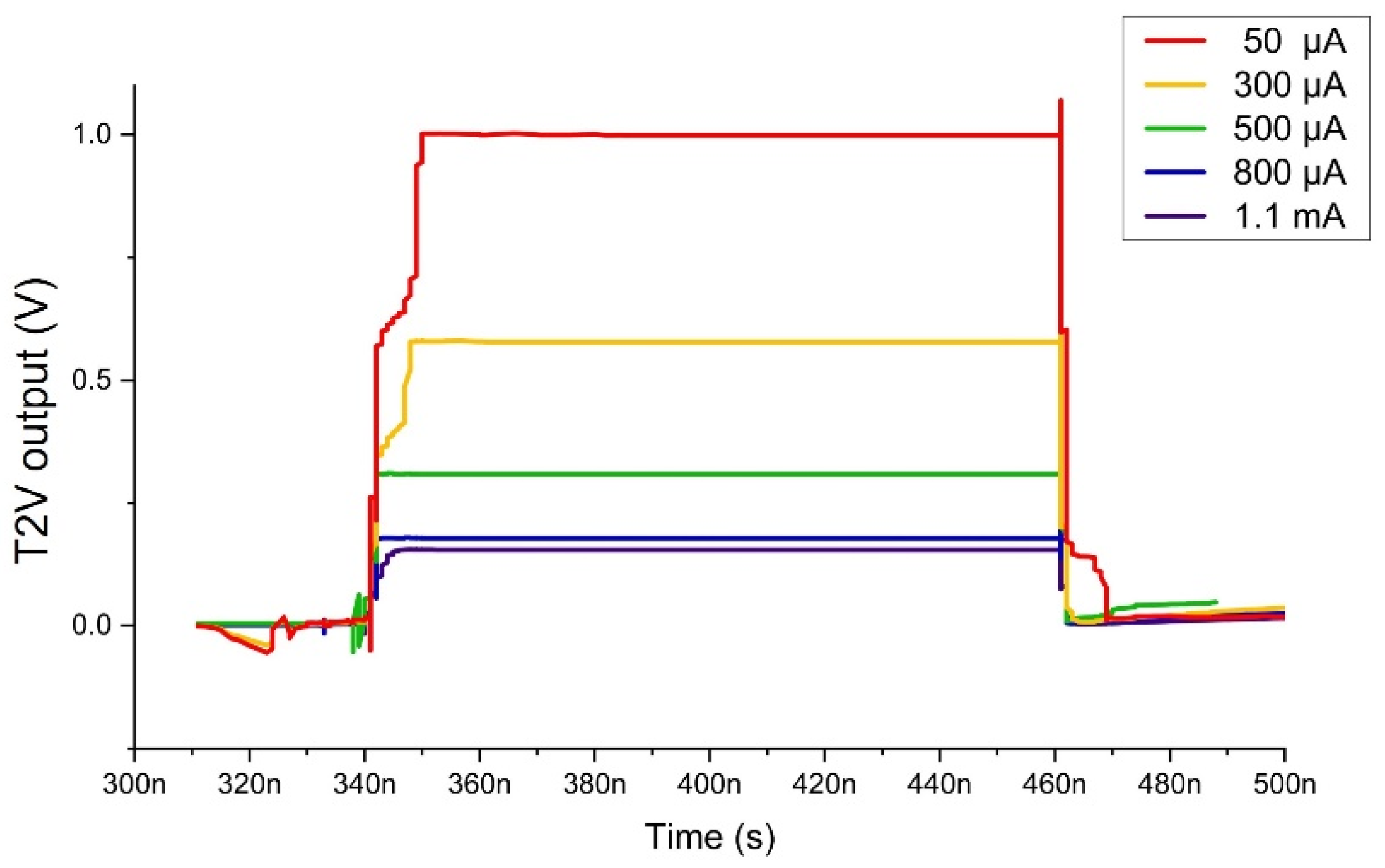
Figure 7 shows the post-layout simulation results of the T2V converter for the input currents of 50 μA
pp ~ 1.1 mA
pp that indicates the minimum detection range of 56 centimeters. Hence, the proposed ORA acquires 27-dB input dynamic range with a linear output over time for each 10-ns time interval, which corresponds to the minimum detection range of 56 centimeters and the maximum detection range of 8.2 meters.
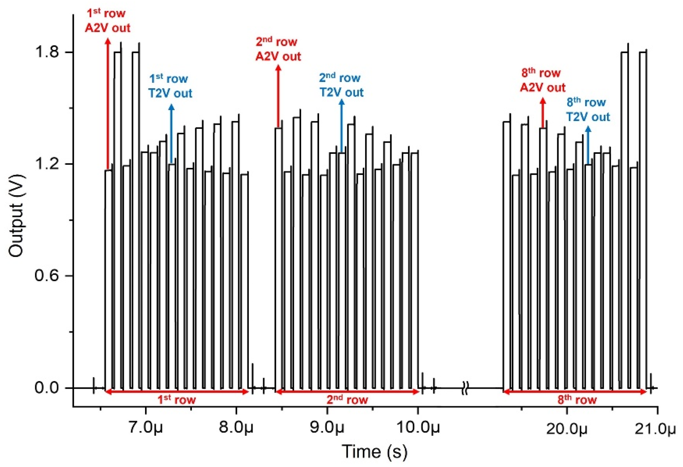
Figure 8 illustrates the simulated pulse response of the proposed 8 x 8 ORA, where the final outputs of three rows (1st, 2nd, and 8th rows) are selected as an example. In each row, the first column of the A2V and T2V outputs are generated and then the rest column signals are consecutively followed. Then, a reset signal is generated after the 8th row for the next optical pulses.
3. Chip Fabrication and Measurements
Test chips of the proposed ORA were realized in a 180-nm CMOS process.
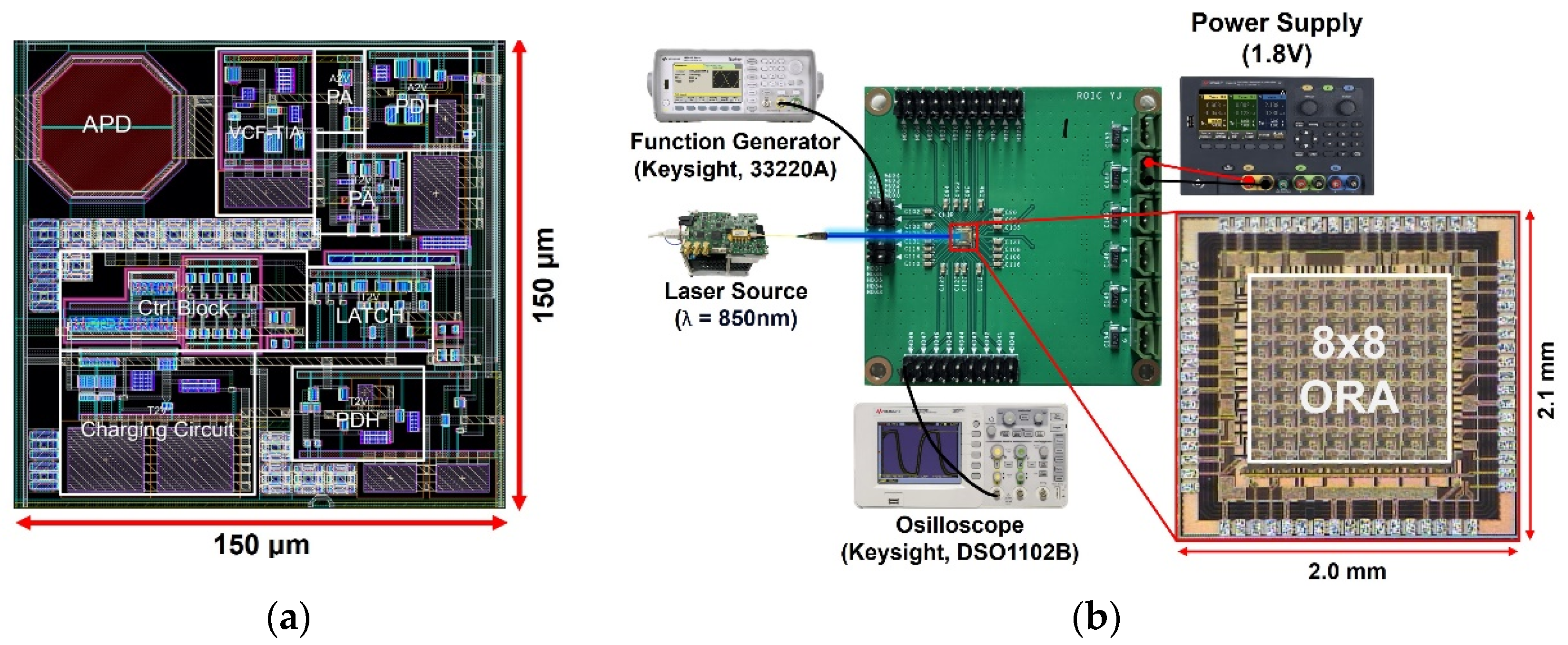
Figure 9a depicts the layout of the proposed 8x8 ORA with on-chip P
+/N-well APDs, where a single-channel occupies the core area of 150 x 150 μm
2, and the whole chip occupies the area of 2.1 x 2.0 mm
2 including I/O pads.
Figure 9b shows the test setup for the proposed 8x8 ORA chip, where the output pulses are measured using an oscilloscope (Keysight DSO1102B), the input signals are generated through a laser source driver (Seed LDD, Notice Ltd.) that is equipped with a laser diode (QPhotonics, USA) operating at the wavelength of 850 nm and producing optical pulse signals with the pulse width of 10 ns.
Figure 10 and
Figure 11 demonstrate the measured results of A2V and T2V of the 8x8 ORA chip for different input currents.
Figure 8 demonstrates the measured outputs of the proposed A2V converter path for three different input currents, indicating an almost linear increase with respect to the input currents, as anticipated at the simulations. Therefore, it can recover the input currents of 5~500 μA
pp with gain control scheme, which corresponds to the minimum detection range of 82.5 centimeters and the maximum detection range of 8.2 meters.
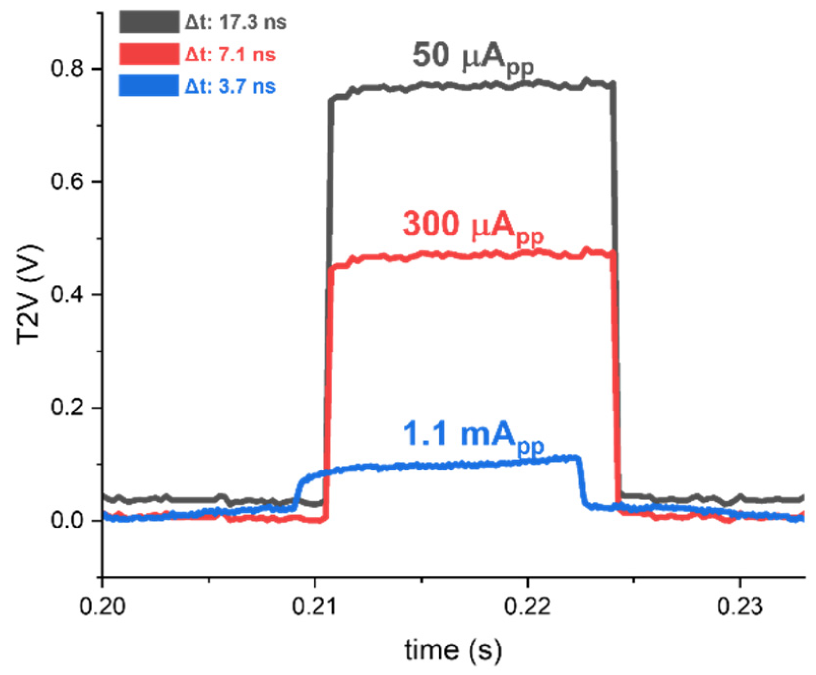
Figure 11 reveals the measured output waveforms of the proposed T2V converter circuit for three different input currents, where the highest peak is acquired for the smallest input current of 50 μA
pp, thereby indicating the detection of a sudden movement (e.g., a fall accident of an elderly patient at a longer distance of 2.6 meters). For a large input current of 1.1 mA
pp, the peak voltage of the output pulse become low, reflecting the detection of movement at a shorter distance. Hence, the proposed T2V converter can acquire 26.8 dB input dynamic range with a linear voltage step of 255 mV for each 10-ns time interval, as shown in the simulations. These results correspond to the minimum detection range of 56 centimeters and the maximum detection range of 2.6 meters.
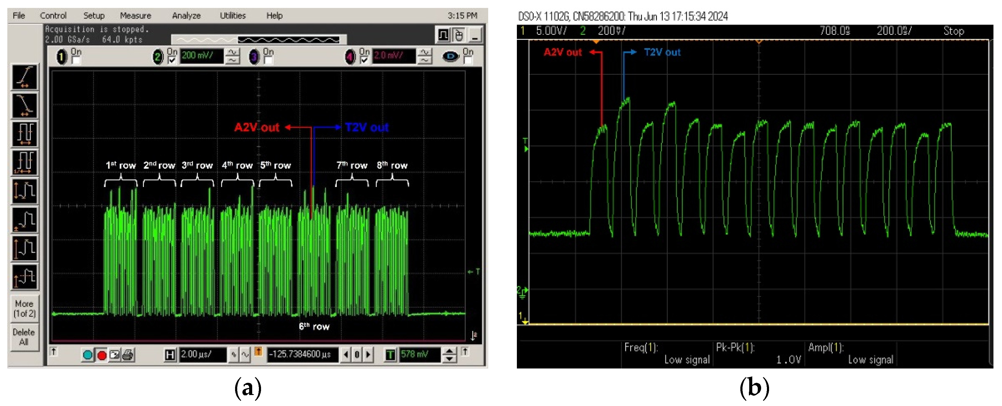
Figure 12 shows the measured pulse response of the proposed 8 x 8 ORA. In
Figure 12a, the final outputs of all the rows (from 1st to 8th rows) are demonstrated and the eight pulses of A2V outputs are followed by those of the T2V outputs in each row.
Figure 12b shows the magnified picture of a single row, where each A2V and T2V signal is clearly measured. Conclusively, the proposed A2V and T2V converters operate complementarily to ensure to generate stable output pulses. The A2V converter extracts intensity (i.e., amplitude) information of the signals, while the T2V converter captures the pulse width information corresponding to the measured distance.
Table 1 compares the performance of the proposed optoelectronic receiver IC with prior arts. Ref. [
14] realized a frequency-compensated voltage-mode inverter TIA that could successfully achieve very low noise current spectral density. However, it mandated high-power dissipation and a large reverse bias of 200 V was necessary for the utilized off-chip APD to acquire 50-A/W responsivity. Also, the maximum detectable input current was obtained by saturating the combination of TIA and PA, and unfortunately, no output waveforms were demonstrated for the large input currents. Ref. [
20] suggested a capacitive feedback TIA equipped with a dual-gain mode for gain-control mechanism. It successfully reduced the input referred noise current with a small bandwidth and extended the dynamic range by utilizing constant-delay detection method. However, it consumed a large chip area and a high power. Also, it required an on-chip high-pass filter to remove low-frequency noises and an off-chip InGaAs APD operating at 1,550 nm with a high responsivity of 5 A/W. Ref. [
21] presented a resistive feedback TIA with a replica circuit followed by a cascaded variable gain amplifier for gain-control, where the bandwidth was considerably reduced to achieve low noise. Also, it exploited a timing discriminator with differential voltage shifters to compensate walk errors. However, it demanded a large power dissipation. Ref. [
22] exploited a differential capacitive-feedback TIA with a very narrow 15-MHz bandwidth that is followed by a differential post-amplifier with offset cancellation, hence providing low-noise characteristics despite the low responsivity of the APD. Yet, this receiver occupied a large chip area, and also was placed on a PC-board with a separate TDC chip with two external comparators to achieve wide dynamic range. Yet, the maximum detectable current was limited to 680 μA
pp only. Ref. [
23] demonstrated a differential voltage-mode TIA utilizing an off-chip APD with 40-A/W responsivity, achieving high transimpedance gain and a very large maximum detectable input current of 39 mA
pp. However, it not only required AC coupling capacitors and bias resistors for the interconnection between the off-chip APD and the receiver, but also mandated a separate TDC chip for maximum input dynamic range as well. Ref. [
24] suggested a common-gate current-mirror TIA with off-chip gain-control to increase the linear accuracy, which is then followed by a high-speed peak detector sample and hold circuit to improve the accuracy further. However, it mandated a programming FPGA-based gain-control to extend the dynamic range characteristic and the linear accuracy.
Hence, this work shows competent performance despite the low-responsivity of the on-chip CMOS APD and the low transimpedance gain characteristics. In particular, it achieves wide dynamic range even without the need of automatic-gain control by the action of the proposed T2V converter. Also, it provides very low power dissipation and small chip area characteristics, therefore enabling the feasible realization of a low-cost low-power LiDAR sensor.
4. Conclusions
We have demonstrated an 8x8 ORA implemented by using a 180-nm CMOS technology. An on-chip CMOS P+/N-well APD is integrated in each cell, enabling to avoid unwanted signal distortion from bond-wires and ESD protection diodes. Also, we have suggested several circuit techniques, including A2V converter to reduce the notorious walk-errors by intensity compensation, and T2V converter to acquire the linear slope of the output signals by exploiting a charging circuit, hence extending the input dynamic range characteristics significantly from 5 μApp to 1.1 mApp, i.e., 48.6 dB. Thise dynamic range corresponds to the maximum detection range of 8.2 meters by the action of the A2V converter and the minimum detection range of 56 centimeters with the aid of the proposed T2V converter. Optically measured results utilizing an 850-nm laser diode confirm that the proposed ORA successfully recovers narrow 5-ns light pulses even at the short distance of 56 centimeters. Hence, this work provides a potential solution for low-cost, low-power short-range LiDAR sensors.
Author Contributions
Conceptualization, S. -M. P.; methodology, Y. C., S. C., J. J., S. -M. P.; validation, Y. C., S. C., J. J.; writing—original draft preparation, S. -M. P.; writing—review and editing, Y. C., S. C., S. -M. P..; visualization, Y. C., S. C., J. J.; supervision, S. -M. Park; project administration, S. -M. Park; funding acquisition, S. -M. Park. All authors have read and agreed to the published version of the manuscript.
Funding
This work was supported by the MSIT (Ministry of Science and ICT), Republic of Korea, under the ITRC (Information Technology Research Center) support program (IITP-2020-0-01847) supervised by the IITP (Institute for Information and Communications Technology Planning and Evaluation). Also, this work was supported by the National Research Foundation (NRF), Korea, under project BK21 FOUR. The EDA tool and chip fabrication were supported by the IC Design Education Center.
Institutional Review Board Statement
Not applicable.
Informed Consent Statement
Not applicable.
Acknowledgments
This work was supported by the National Research Foundation (NRF), Korea, under project BK21 FOUR. The EDA tool and chip fabrication were supported by the IC Design Education Center.
Conflicts of Interest
The authors declare no conflict of interest.
References
- D. Yoon, J.-E. Joo, and S. M. Park, “Mirrored Current-Conveyor Transimpedance Amplifier for Home Monitoring LiDAR Sensors,” IEEE Sensors J., vol. 21, no. 5, pp. 5589–5597, Mar. 2021. [CrossRef]
- N. Frøvik, B. A. Malekzai, and K. Øvsthus, “Utilising LiDAR for fall detection,” Healthcare Technology Letters, vol. 8, no. 1, pp. 11–17, 2021. [CrossRef]
- P. Fraccaro, X. Evangelopoulos, and B. Edwards, “Development and Preliminary Evaluation of a Method for Passive, Privacy-Aware Home Care Monitoring Based on 2D LiDAR Data,” in Artificial Intelligence in Medicine, Cham, 2020, pp. 160–169. [CrossRef]
- Y.-T. Wang, C.-C. Peng, A. A. Ravankar, and A. Ravankar, “A Single LiDAR-Based Feature Fusion Indoor Localization Algorithm,” Sensors, vol. 18, no. 4, Art. no. 4, Apr. 2018. [CrossRef]
- C. Medina Sánchez, M. Zella, J. Capitán, and P. J. Marrón, “From Perception to Navigation in Environments with Persons: An Indoor Evaluation of the State of the Art,” Sensors (Basel), vol. 22, no. 3, p. 1191, Feb. 2022. [CrossRef]
- C. Hong, S.-H. Kim, J.-H. Kim, and S. M. Park, “A Linear-Mode LiDAR Sensor Using a Multi-Channel CMOS Transimpedance Amplifier Array,” IEEE Sensors J., vol. 18, no. 17, pp. 7032–7040, Sep. 2018. [CrossRef]
- T.-H. Ngo, C.-H. Kim, Y. J. Kwon, J. S. Ko, D.-B. Kim, and H.-H. Park, “Wideband Receiver for a Three-Dimensional Ranging LADAR System,” IEEE Tran. on Circuits and Systems I: Regular Papers, vol. 60, no. 2, pp. 448–456, Feb. 2013. [CrossRef]
- F. Khoeini, B. Hadidian, K. Zhang, and E. Afshari, “A Transimpedance-to-Noise Optimized Analog Front-End With High PSRR for Pulsed ToF Lidar Receivers,” IEEE Tran. on Circuits and Systems I: Regular Papers, vol. 68, no. 9, pp. 3642–3655, Sep. 2021. [CrossRef]
- H. Zheng, R. Ma, M. Liu, and Z. Zhu, “High Sensitivity and Wide Dynamic Range Analog Front-End Circuits for Pulsed TOF 4-D Imaging LADAR Receiver,” IEEE Sensors J., vol. 18, no. 8, pp. 3114–3124, Apr. 2018. [CrossRef]
- H. Zheng, R. Ma, X. Wang, D. Li, J. Hu, Y. Liu, and Z. Zhu, “A Linear-Array Receiver AFE Circuit Embedded 8-to-1 Multiplexer for Direct ToF Imaging LiDAR Applications,” IEEE Tran. on Circuits and Systems I: Regular Papers, pp. 1–9, 2022. [CrossRef]
- P. Wang, M. Ye, X. Xia, X. Zheng, Y. Li, and Y. Zhao, “A Multi-Channel Low-Noise Analog Front End Circuit for Linear LADAR,” IEEE Tran. on Circuits and Systems II: Express Briefs, vol. 67, no. 7, pp. 1209–1213, Jul. 2020. [CrossRef]
- H. Zheng, K. Li, and J. Guo, “Analog Front-End Circuits With Input Current Attenuation and Heterodyne Techniques for Low-Cost Phase-Shift LADAR Receiver,” IEEE Sensors J., vol. 21, no. 6, pp. 7813–7824, Mar. 2021. [CrossRef]
- J.-E. Joo, M.-J. Lee, and S. M. Park, “A CMOS Optoelectronic Receiver IC with an On-Chip Avalanche Photodiode for Home-Monitoring LiDAR Sensors,” Sensors, vol. 21, no. 13, Art. no. 13, Jan. 2021. [CrossRef]
- X. Wang, R. Ma, D. Li, H. Zheng, M. Liu, and Z. Zhu, “A Low Walk Error Analog Front-End Circuit With Intensity Compensation for Direct ToF LiDAR,” IEEE Tran. on Circuits and Systems I: Regular Papers, vol. 67, no. 12, pp. 4309–4321, Dec. 2020. [CrossRef]
- M. Hintikka and J. Kostamovaara, “A 700 MHz laser radar receiver realized in 0.18 μm HV-CMOS,” Analog Integrated Circuits and Signal Processing, vol. 93, no. 2, pp. 245–256, Nov. 2017. [CrossRef]
- V. N. Nguyen, D. N. Duong, Y. Chuang, and J. -W. Lee, “A Cyclic Vernier Two-Step TDC for High Input Range Time-of-Flight Sensor Using Startup Time Correction Technique,” Sensors, vol. 18, pp. 3948, Nov. 2018. [CrossRef]
- Y. He and S. M. Park, “A CMOS Integrator-Based Clock-Free Time-to-Digital Converter for Home-Monitoring LiDAR Sensors,” Sensors, vol. 22, pp. 554, Jan. 2022. [CrossRef]
- M. Liu, H. Liu, X. Li, and Z. Zhu, “A 60-m Range 6.16-mW Laser Power Linear-Mode LiDAR System with Multiplex ADC/TDC in 65-nm CMOS,” IEEE Trans. Circuits Syst. I Reg. Pap., vol. 67, pp. 753–764, Mar. 2020. [CrossRef]
- M.-J. Lee and W.-Y. Choi, “Performance Optimization and Improvement of Silicon Avalanche Photodetectors in Standard CMOS Technology,” IEEE J. of Selected Topics in Quantum Electronics, vol. 24, no. 2, pp. 1–13, Mar. 2018. [CrossRef]
- H. -S. Cho, C. -H. Kim, and S. -G. Lee, “A High-Sensitivity and Low-Walk Error LADAR Receiver for Military Application,” IEEE Transactions on Circuits and Systems I: Reg. Pap., vol. 61, no. 10, pp. 3007-3015, Oct. 2014. [CrossRef]
- H. Zheng, R. Ma, M. Liu, and Z. Zhu, “A Linear Dynamic Range Receiver With Timing Discrimination for Pulsed TOF Imaging LADAR Application,” IEEE Trans. on Instrumen. and Meas., vol. 67, no. 11, pp. 2684-2691, Nov. 2018. [CrossRef]
- S. Kurtti, A. Baharmast, J. -P. Jansson, and J. Kostamovaara, “A Low-Noise and Wide Dynamic Range 15 MHz CMOS Receiver for Pulsed Time-of-Flight Laser Ranging,” IEEE Sensors J., vol. 21, no. 20, pp. 22944-22955, Oct. 2021. [CrossRef]
- S. Kurtti, J. -P. Jansson, and J. Kostamovaara, “A CMOS Receiver–TDC Chip Set for Accurate Pulsed TOF Laser Ranging,” IEEE Tran. on Instrumen. and Meas., vol. 69, no. 5, pp. 2208–2217, May 2020. [CrossRef]
- R. Ma, M. Liu, H. Zheng, and Z. Zhu, “A 66-dB linear dynamic range 100dBΩ transimpedance gain TIA with high-speed PDSH for LiDAR,” IEEE Tran. on Instrumen. and Meas., vol. 69, no. 4, pp. 1020-1028, Apr. 2020. [CrossRef]
|
Disclaimer/Publisher’s Note: The statements, opinions and data contained in all publications are solely those of the individual author(s) and contributor(s) and not of MDPI and/or the editor(s). MDPI and/or the editor(s) disclaim responsibility for any injury to people or property resulting from any ideas, methods, instructions or products referred to in the content. |
© 2024 by the authors. Licensee MDPI, Basel, Switzerland. This article is an open access article distributed under the terms and conditions of the Creative Commons Attribution (CC BY) license (http://creativecommons.org/licenses/by/4.0/).
